1. Introduction
In this work we present a numerical investigation of slot waveguides for evanescent field infrared absorption sensing of CO
2. Slot waveguides were first theoretically described in [
1], and experimentally demonstrated in [
2]. Slot waveguides offer the advantage of an increased electric field in the slot that leads to a high evanescent field ratio, which is specifically beneficial for gas sensing applications. If CO
2 is present in the slot, the evanescent field is partially absorbed by the gas, which is detected in terms of an associated damping of the guided wave. In [
3], a numerical investigation of slot waveguides for CO
2 sensing using a silicon on sapphire platform was presented and an evanescent field ratio as high as ~25% was reported.
Our approach is to use SiO
2 and Si
3N
4 as materials for the lower cladding region of the waveguide. Recently we experimentally demonstrated silicon strip waveguides for CO
2 sensing using two different platforms, i.e., silicon strip waveguides on a Si3N4 membrane [
4] and on a solid (Si
3N
4)/SiO
2 substructure [
5]. In order to further improve the sensing performance of the waveguide structure, we aim to develop Si slot waveguides on SiO
2 with a significantly higher evanescent field ratio compared to the strip waveguides that were used in our previous work.
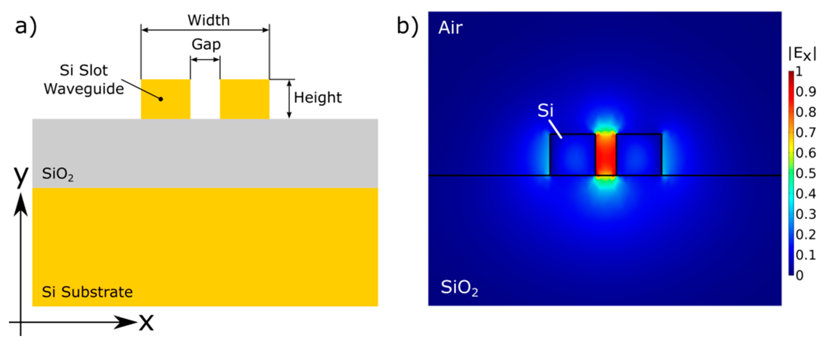
Figure 1 shows a schematic representation of the slot waveguide (a) and a representative field distribution of a quasi-TE mode (b), showing strong confinement of the electric field in the slot. The investigated sensor structures are compatible to fabrication on SOI wafers or on standard silicon substrates using deposited SiO
2 as substructure materials and deposited poly-silicon as waveguide material. Our ultimate goal is to develop a micro-sensor fully integrated on standard silicon substrates. Therefore, the waveguides were optimized using material parameters that were measured on deposited thin films of poly-Si and SiO
2. The waveguides were optimized for a wavelength of λ = 4.26 µm, which is at the center of the mid-infrared absorption band of CO
2 and for a gap size of 300 nm, which is compatible with standard micro fabrication processes.
2. Method
The FEM simulations were conducted using COMSOL Multiphysics 5.3a including the Wave Optics Module. The slot waveguides were investigated using full-vectorial FEM simulations. The domain size was 10 µm in x and y direction and was enclosed by perfectly matched layers and scattering boundary conditions in order minimize spurious reflections at the boundaries. So called “Numerical Ports” were applied on both ends of the waveguide which allow to calculate, excite and absorb specific modes. The cross-section of model was meshed with triangular elements with a maximum size of λ/(8*n), where λ is the wavelength and n the refractive index of the individual material. Along the propagation direction the mesh of the cross-section was swept with a maximum element size of λ/(8*nSi). The required optical parameters (i.e., the complex refractive index) of the used materials (SiO2 and poly-Si) were measured on thin films prepared by low pressure chemical vapor deposition. The optical parameters were measured using a J.A. Woollam IR VASE ellipsometer.
3. Results and Discussion
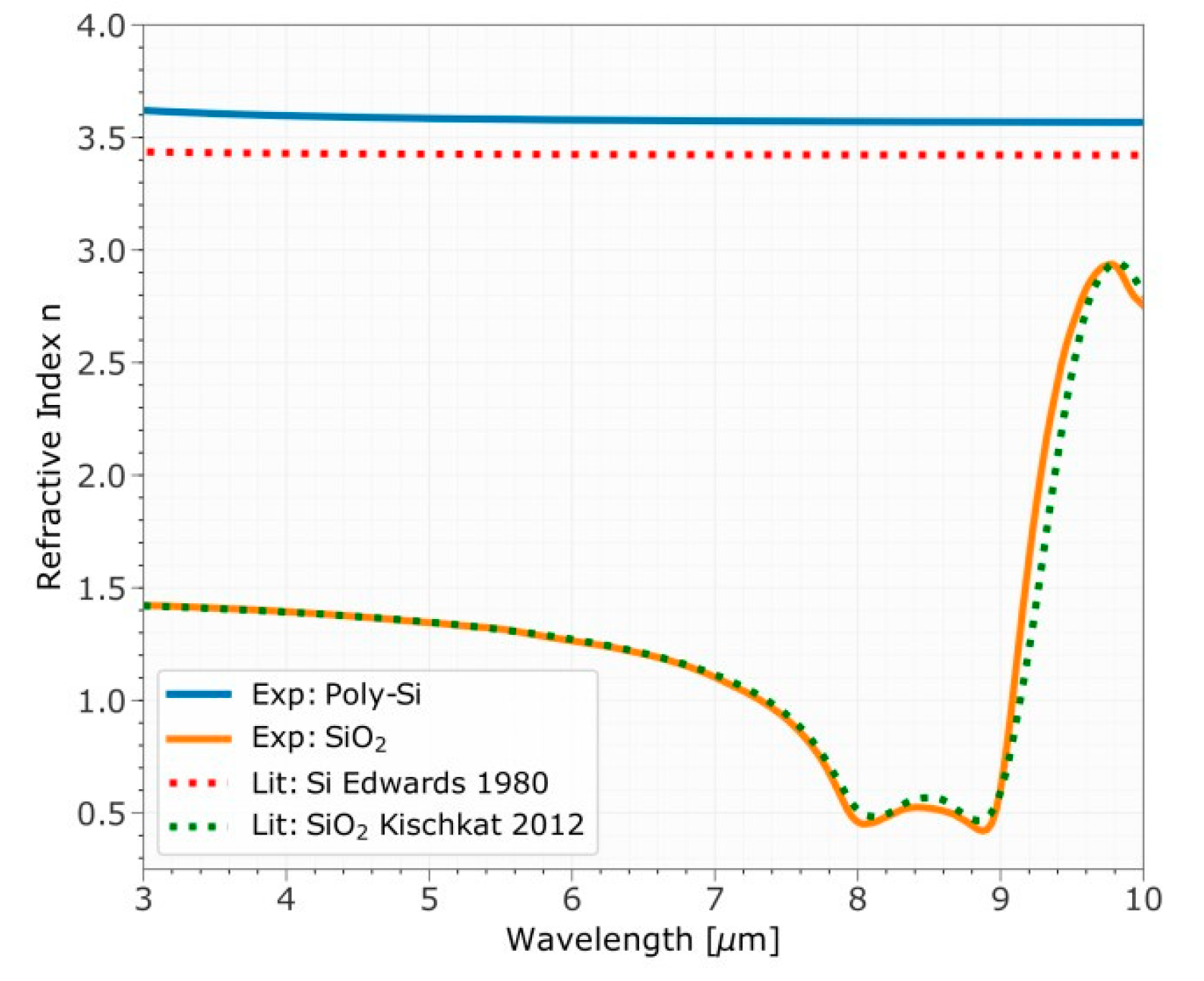
The real part of the measured refractive index for poly-Si and SiO
2 is plotted in
Figure 2. While the experimental results were in very good agreement with literature for SiO
2 [
6], poly-Si had a higher refractive index than previously reported for bulk silicon [
7]. As described, the waveguides were designed for a wavelength of 4.26 µm. The measured real part of the refractive indices at this wavelength are n
Si = 3.60 and n
SiO2 = 1.38. The imaginary part (also known as extinction coefficient) at this wavelength is virtually zero for silicon and was at the noise level of the ellipsometry measurement of SiO
2. Therefore, the extinction coefficients were not considered, meaning that losses caused by absorption in the material were not considered in the simulation.
A 3D model of the slot waveguide was developed using COMSOL Multiphysics. The effective mode indices of the fundamental quasi-TE mode were determined conducting a modal analysis on the cross-section of the waveguide (see
Figure 3a), searching for the two lowest order modes of the waveguide (modes with the highest effective mode indices). The waveguides were investigated for a gap width of 300 nm. It was found that for geometries with high aspect ratios (height/width) the fundamental mode of the waveguide is the quasi-TM mode, i.e., the mode with the highest effective mode index (not plotted). Furthermore, modes for some geometries with small waveguide widths do not fulfill the condition for guided modes (
nwaveguide >
neff >
ncladding) [
8]. These modes, i.e., modes with an effective index smaller than the refractive index of SiO
2, will leak out and do not propagate over wide ranges in the slot waveguide.
Figure 3c ‘1’ shows a field distribution of such a mode. It is visible that a significant part of the mode is present in the SiO2. The evanescent field ratio (EFR), which is a crucial parameter for the sensing application, was determined using the following equation [
3]
where the surface integrals extend over (parts of) the cross-sectional xy-plane of the waveguide, denotes the Poynting vector and the unit normal vector pointing in the direction of propagation.
The results are shown in
Figure 3b. The highest EFR among the tested configurations was 42% for a waveguide height of 800 nm and a width of 1500 nm (see also the field distribution plotted in
Figure 3c ‘2’). If the width of the waveguide is further increased, the fraction of the mode that is confined in the silicon part increases, which decreases the EFR of the mode (see
Figure 3b and also
Figure 3c ‘3’). As indicated in
Figure 3b, choosing a higher aspect ratio leads to a higher EFR. Nevertheless, a high aspect ratio also favors the propagation of quasi-TM modes. Already for a Si height of 900 nm, the fundamental quasi-TE mode is no longer among two lowest order modes (not plotted).
4. Conclusions
A numerical study on slot waveguides for gas sensing, using a Si on SiO2 platform, was presented. The evanescent field ratio, which is a crucial parameter for the application of waveguides as absorption sensor, was determined. The highest evanescent field ratio that was obtained was 42%. In conclusion, this study indicates that silicon slot waveguides on a SiO2 are promising candidates for integrated evanescent field gas sensors.
Acknowledgments
This work was performed within the Competence Centre ‘ASSIC Austrian Smart Systems Integration Research Center’ and ‘LCM Linz Centre of Mechatronics’, co-funded by the Federal Ministries of Transport, Innovation and Technology (BMVIT) and Digital and Economic Affairs (BMDW) and the Federal Provinces of Carinthia, Styria and Upper Austria within the COMET—Competence Centers for Excellent Technologies Programme. The authors would like to thank Markus Bergmeister for the support with the thin film samples and furthermore Kurt Hingerl and Reza Sharif for the support with the ellipsometry measurements.
Conflicts of Interest
The authors declare no conflict of interest. The founding sponsors had no role in the design of the study; in the collection, analyses, or interpretation of data; in the writing of the manuscript, and in the decision to publish the results.
References
- Almeida, V.R.; Xu, Q.; Barrios, C.A.; Lipson, M. Guiding and confining light in void nanostructure. Opt. Lett. 2004, 29, 1209. [Google Scholar] [CrossRef]
- Xu, Q.; Almeida, V.R.; Panepucci, R.R.; Lipson, M. Experimental demonstration of guiding and confining light in nanometer-size low-refractive-index material. Opt. Lett. 2004, 29, 1626. [Google Scholar] [CrossRef] [PubMed]
- Huang, Y.; Kalyoncu, S.K.; Zhao, Q.; Torun, R.; Boyraz, O. Silicon-on-sapphire waveguides design for mid-IR evanescent field absorption gas sensors. Opt. Commun. 2014, 313, 186–194. [Google Scholar] [CrossRef]
- Ranacher, C.; Consani, C.; Tortschanoff, A.; Jannesari, R.; Bergmeister, M.; Grille, T.; Jakoby, B. Mid-infrared absorption gas sensing using a silicon strip waveguide. Sens. Actuators A Phys. 2018, 277, 117–123. [Google Scholar] [CrossRef]
- Ranacher, C.; Consani, C.; Vollert, N.; Tortschanoff, A.; Bergmeister, M.; Grille, T.; Jakoby, B. Characterization of Evanescent Field Gas Sensor Structures Based on Silicon Photonics. IEEE Photonics J. 2018, 10, 1–4. [Google Scholar] [CrossRef]
- Kischkat, J.; Peters, S.; Gruska, B.; Semtsiv, M.; Chashnikova, M.; Klinkmüller, M.; Fedosenko, O.; Machulik, S.; Aleksandrova, A.; Monastyrskyi, G.; et al. Mid-infrared optical properties of thin films of aluminum oxide, titanium dioxide, silicon dioxide, aluminum nitride, and silicon nitride. Appl. Opt. 2012, 51, 6789. [Google Scholar] [CrossRef] [PubMed]
- Edwards, D.F.; Ochoa, E. Infrared refractive index of silicon. Appl. Opt. 1980, 19, 4130. [Google Scholar] [CrossRef] [PubMed]
- Ghatak, A.; Thyagarajan, K. An Introduction to Fiber Optics; Cambridge University Press: Cambridge, UK, 1998; ISBN 978-0-521-57785-4. [Google Scholar]
| Publisher’s Note: MDPI stays neutral with regard to jurisdictional claims in published maps and institutional affiliations. |
© 2018 by the authors. Licensee MDPI, Basel, Switzerland. This article is an open access article distributed under the terms and conditions of the Creative Commons Attribution (CC BY) license (https://creativecommons.org/licenses/by/4.0/).


