Abstract
Passive and wireless SAW sensors can operate in extreme environment. However, there is no mass-market application for this technology yet, due notably to the lack of an adequate sensor housing solution. Package-less SAW sensors are therefore promising. Here, guided waves that propagate in a protective multilayer structure are used, instead of SAWs. However, issues will arise from the use of a multilayer structure. In particular, thermo-mechanical effects will impact the behavior of the devices. A solution must also be found to embed the antenna in the stack. We present here the results of a numerical study of the thermo-mechanical effects, in two package-less structures. One possible antenna design is proposed and evaluated.
1. Introduction
AlN/ZnO/IDT/LNY+128 (S1) and AlN/IDT/LNY+128 (S2) are among the most promising multilayer structures that have been suggested and studied so far [1,2]. Here, IDT designates the Inter Digital Transducer that is required to convert electrical signals into acoustic waves, and vice versa. S1 and S2 are better suited for sensing applications at lower and higher temperature (>350 °C), respectively. First demonstrators of S1 were tested in 2017, with encouraging results. The fabrication of S2 demonstrators is in progress. In both cases, temperature-triggered issues will arise from the stack structure itself, and from the significantly different temperature coefficients of expansion of AlN, ZnO and Lithium Niobate (LN). If delamination phenomena are expected to make package-less sensors inoperable above one given limit temperature, growing thermo-mechanical stress (and strain) fields will start impacting the sensors behavior and properties at lower temperature already. They might also degrade the guiding properties, in the S2 configuration particularly. Indeed, if acoustic impedance mismatch between the layers is the only mechanism used to guide the waves in the S1 configuration (the waves are guided in the low impedance ZnO layer, surrounded by two high impedance layers), the guiding effect in S2 is due to the slow-down of the waves using heavy Pt electrodes and to the particular crystallographic properties of the LNY + 128 substrate. A change in the crystallographic properties due to thermo-mechanical stress and strain fields might therefore result in partial or complete loss of the guiding properties. It is therefore important to evaluate the expected effects of thermo-mechanical stress and strain fields on the guiding properties, in a wide temperature range.
The use of a thinner LNY + 128 wafer being an interesting option to achieve ultra-thin wearable sensors, it is also important to check the impact of wafer-thinning on the sensor’s performances.
The first section of the paper is therefore dedicated to the study of the effect of growing thermo-mechanical stress and strain fields in S1 and S2, versus temperature and LN thickness. The guiding properties of S2 were also checked, up to 100 °C. The computations were performed using COMSOL Multiphysics.
In the second section, a concept of an embedded antenna is presented, for the S1 configuration. The antenna is embedded in the multilayer structure itself. It is therefore located between two layers of highly different dielectric properties, which complicate the computation and optimization of its gain and radiation pattern. The gain, radiation pattern and S11 parameters of the antenna were computed using EMPro (Keysight), for one set of layer thicknesses. The expected time response of an ideal 2.45 GHz reflective Delay Line (R-DL) based on the S1 configuration was also computed, using proprietary software. Although promising, the results show that it wouldn’t be possible to interrogate the R-DL equipped with the proposed antenna, as the antenna gain is still way too low.
2. Thermo-Mechanical Effects
2.1. Thermo-Mechanical Stress Fields
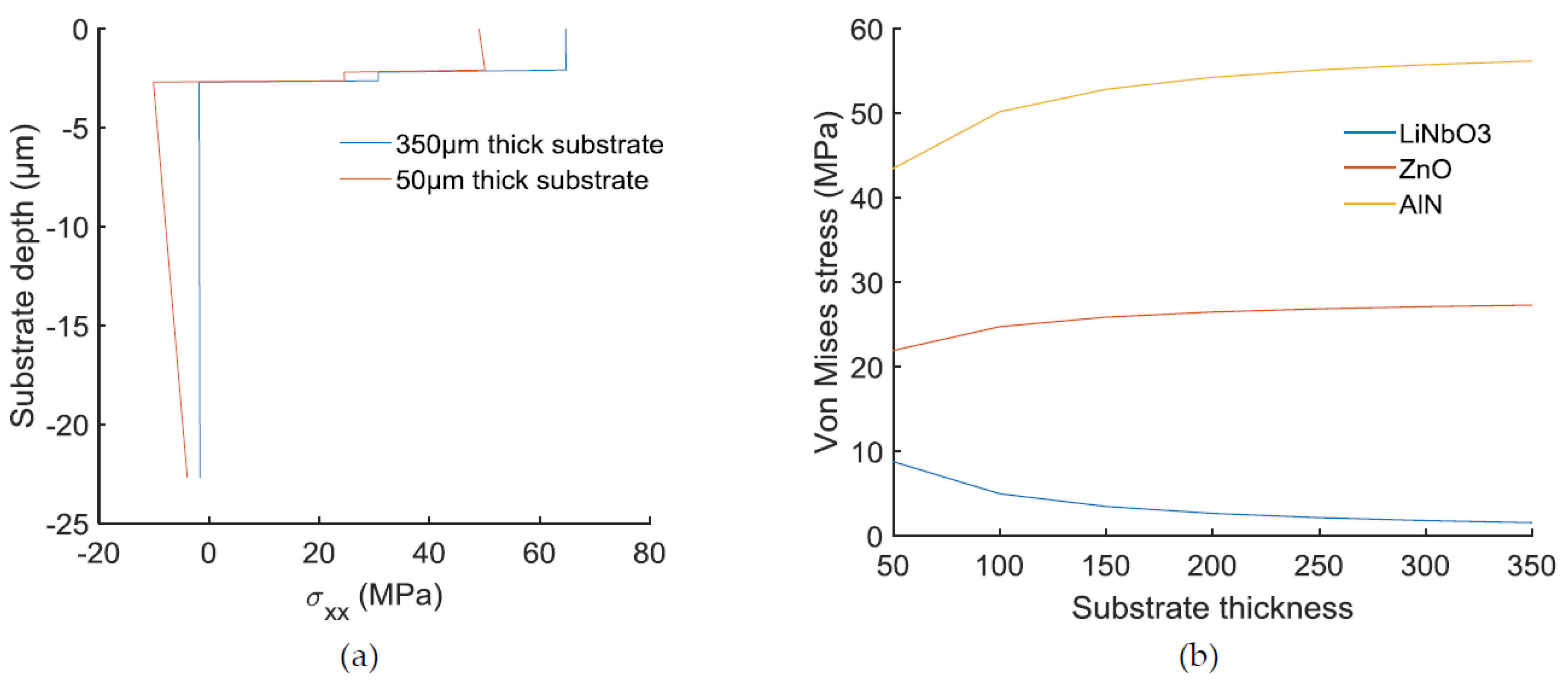
The stress fields generated in S1 by a temperature increase of only 20 °C (with 50 and 350 µm-thick LN) are shown in Figure 1a. The evolution of the Von Mises stress in the layers versus substrate thickness is shown in Figure 1b.
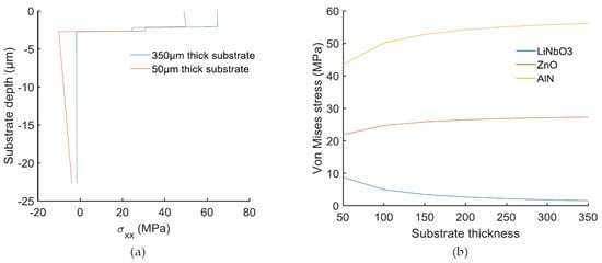
Figure 1.
(a) Thermo-mechanical stress field σxx generated in the AlN/ZnO/LNY + 128° (S1) structure, by a temperature increase of 20 °C. Two thicknesses of LN are considered here: 50 µm and 350 µm. (b) Evolution of the Von Mises stress in the layers, versus substrate (LN) thickness.
The Von Mises stress reaches ~50MPa in the AlN layer for a temperature increase of only 20 °C. This is a large value already. Larger levels of stress are expected to cause delamination issues, at higher temperatures. However, the reduction of the LN thickness improves the situation, as thinner substrates impose less deformation on the overlying thin layers (thin substrates are ‘weaker’). This is a promising result for wearable applications, where thin devices are needed.
2.2. Influence on the Guiding Properties
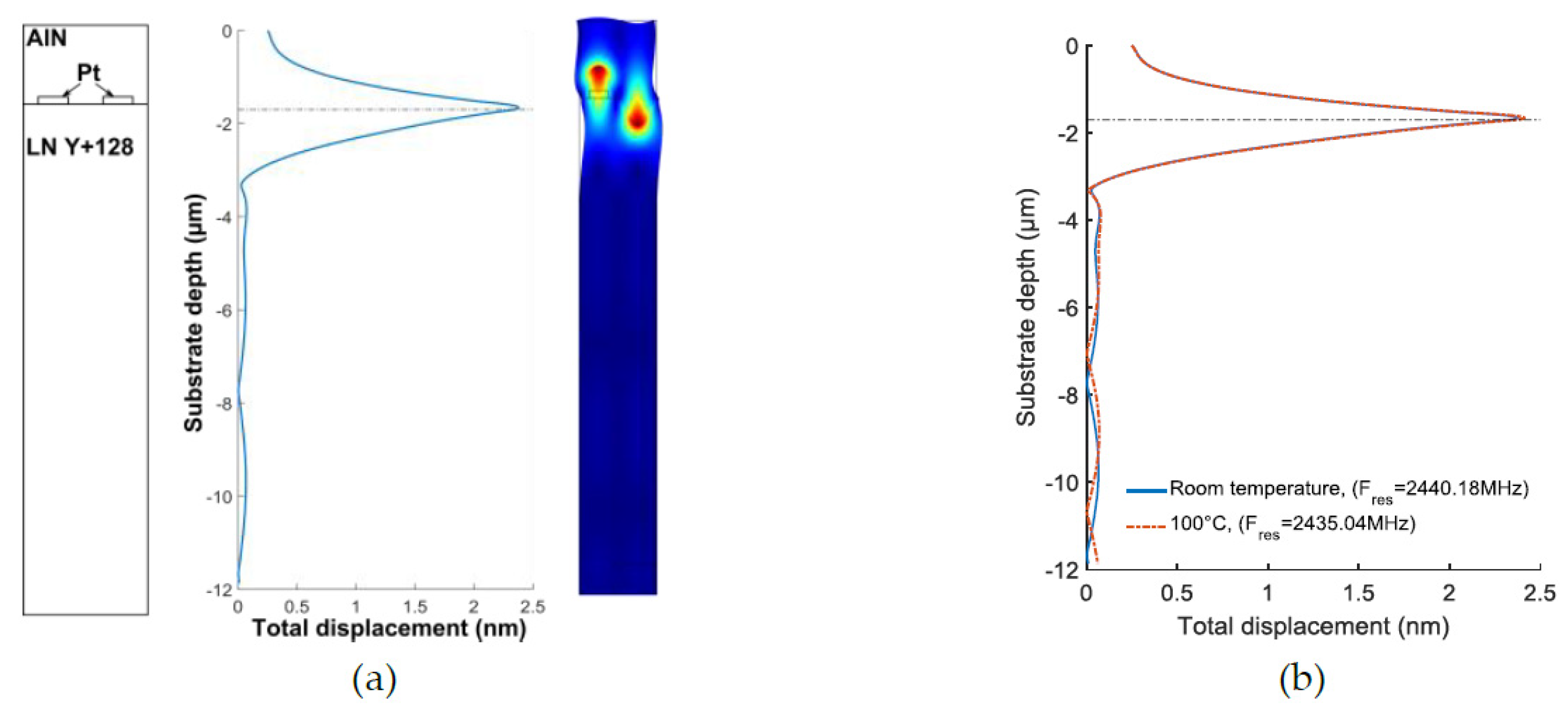
The guiding properties of a S2 stack were checked, at 100 °C (1.7 µm-AlN/200 µm-LNY+128). The thermally-induced stress and strain fields were computed. Simulations of the electroacoustic behavior were performed using a single-cell model. The effects of these thermally-induced fields were taken into account, as well as the effect of temperature alone (see [3] for more details on the computation method). However, as the third-order elastic coefficients of thin AlN layers remain unknown, the influence of strain on the material parameters was considered in the LN substrate only.
The results show that the considered change in temperature has little influence on the displacement profile along the substrate depth (see Figure 2). The wave is still well guided. This makes us confident that the structure should keep its guiding properties, at higher temperature.
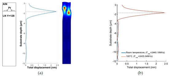
Figure 2.
Guided mode in the S2 configuration. (a) at room temperature. (b) Comparison of the displacement fields, at room temperature and 100 °C. Both fields are almost identical.
3. The Embedded Antenna
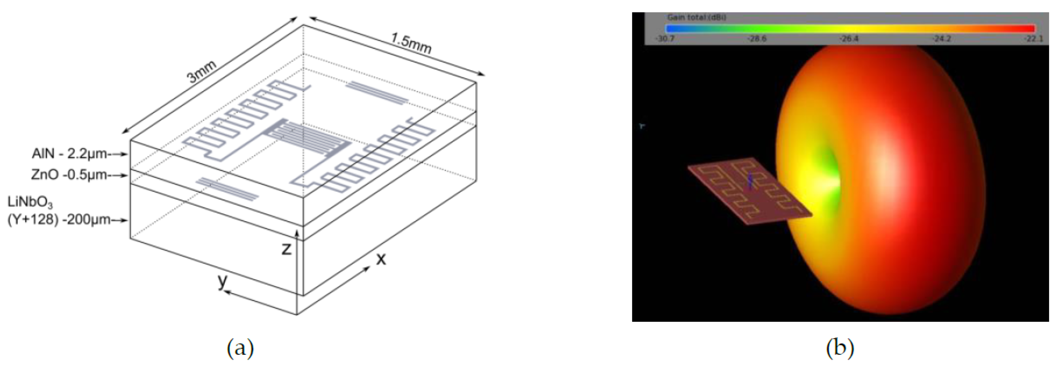
The use of an external antenna (and connection of the IDT to it) constitutes one of the major issues, for package-less SAW sensors. An attractive solution would be to directly embed the antenna in the multilayer structure itself (see Figure 3a). In addition to protecting the antenna and realizing a truly package-less device, it might also make the fabrication of the sensor easier. However, the antenna thickness must be larger than the skin depth of its constituting metal (>1.5 µm for Gold, at 2.45 GHz), which might generate unforeseen issues. In addition to being significantly thicker than the IDT and reflectors (~60 nm at 2.45 GHz), the antenna would also be thicker than the ZnO layer itself. In addition, SAW sensors are much smaller than λ/4 (~3 cm at 2.45 GHz), and the antenna would be located between two layers of highly different dielectric properties. This makes the design of an efficient antenna highly challenging.
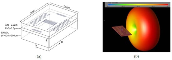
Figure 3.
(a) Schematic description of an innovative AlN/ZnO/IDT/LN package-less SAW sensor, with embedded antenna. (b) Embedded antenna: simulation model and radiation pattern, at 1.97 GHz.
We present here a first study of a dipole-like antenna, to be embedded in the S1 structure. The antenna and its radiation pattern around 2 GHz are presented in Figure 3b. Note that the thickness of the antenna was automatically scaled up above the skin depth, by the simulation software.
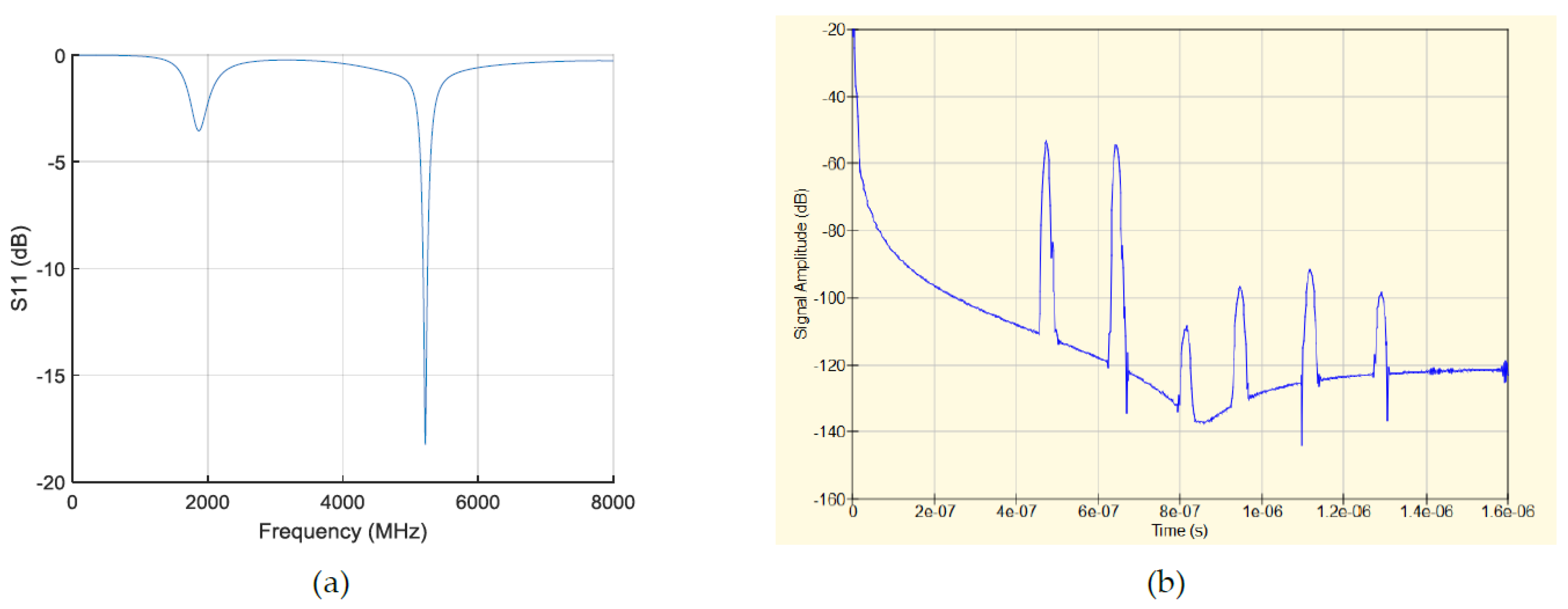
The antenna gain is poor, which is probably due to the presence of the highly dielectric LN substrate, in contact with the antenna. On the contrary, the thin ZnO and AlN layers do not seem to strongly impact the performances of the antenna. The S11 parameters of the antenna in a wider frequency range are shown in Figure 4a. The response in time domain of a typical 2.45 GHz R-DL similar to the one presented in Figure 3a is shown in Figure 4b. The computations were based on recently published COM parameters, for the S1 configuration [4]. It can be seen that the expected level of the two main reflected peaks is already very low (close to −55 dB), without even taking into account the propagation losses in ZnO and AlN! It would therefore be (almost) impossible to extract a useful signal from the sensor, using such a simple antenna.
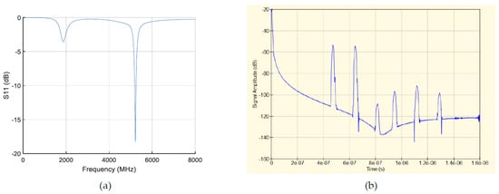
Figure 4.
(a) S11 parameters of the antenna only. (b) Computed time response of a typical reflective Delay-Line in AlN/ZnO/LN, similar to the one presented in Figure 3.a. Note the expected level of the two main peaks, close to −55 dB.
Future work includes a more thorough analysis of the layer-stack/antenna system, as well as the testing and evaluation of existing solutions, to strongly improve the antenna gain in the S1 configuration.
4. Discussion and Conclusion
Fully package-less SAW sensors are highly promising devices. To achieve such a sensor, optimization of their components is required. Especially, the gain of the embedded antenna must be strongly improved. On the other hand, results show that thinner LN wafers should help reduce the amount of thermo-mechanical stress generated at the interfaces, in the multilayer structures. This is encouraging, as thinner sensors are needed for special applications, like wearable sensors. In addition, preliminary simulation results also show that the AlN/LN configuration should maintain its wave-guiding properties in a wide temperature range.
Acknowledgments
This project was partly supported by the COMET K1 center ASSIC Austrian Smart Systems Integration Research Center. The COMET ‘Competence Centers for Excellent Technologies’ program is supported by BMVIT, BMWFW and the federal provinces of Carinthia and Styria.
Conflicts of Interest
The authors declare no conflict of interest. The founding sponsors had no role in the design of the study; in the collection, analyses, or interpretation of data; in the writing of the manuscript, and in the decision to publish the results.
References
- Floer, C.; Moutaouekkil, M.; Bartoli, F.; Mishra, H.; Hage-Ali, S.; McMurtry, S.; Pigeat, P.; Elmazria, O.; Aubert, T.; Zhgoon, S.; et al. AlN/ZnO/LiNbO3 packageless structure as a low-profile sensor for on-body applications. In Proceedings of the IEEE International Ultrasonics Symposium (IUS), Washington, DC, USA, 6–9 September 2017; pp. 1–4. [Google Scholar]
- Naumenko, N.; Nicolay, P. AlN/Pt/LN structure for SAW sensors capable of operating at high temperature. Appl. Phys. Lett. 2017, 111, 073507. [Google Scholar] [CrossRef]
- Chambon, H.; Nicolay, P.; Bruckner, G.; Benjeddou, A. Analysis of the sensitivity to pressure and temperature of a membrane based SAW sensor. Int. J. Smart Nano Mater. 2017, 8, 95–109. [Google Scholar] [CrossRef]
- Chambon, H.; Nicolay, P.; Floer, C.; Benjeddou, A. Package-less SAW RFID sensors for structural health monitoring applications: A concept study. In Proceedings of the 7th International Symposium on Aircraft Materials (ACMA2018), Compiègne, France, 24–26 April 2018; pp. 493–500. [Google Scholar]
Publisher’s Note: MDPI stays neutral with regard to jurisdictional claims in published maps and institutional affiliations. |
© 2018 by the authors. Licensee MDPI, Basel, Switzerland. This article is an open access article distributed under the terms and conditions of the Creative Commons Attribution (CC BY) license (https://creativecommons.org/licenses/by/4.0/).