1. Introduction
The importance of nanostructured surfaces is strongly gaining importance. More and more conferences, funding programs and publications are dealing with this topic confirming its increasing interest. Nanostructures can help to enhance the functionality of surfaces/devices, reduce building volumes, substitute additional coatings and therefore, reduce the costs of production or they can even add new functions.
Beside hot-embossing and nanoimprint lithography, injection moulding is another very potent high-volume production technique which is also capable to reproduce micro- and nanostructures, e.g., for optical storage media. In general, the production of structured nonplanar surfaces is a rarity because of the high demands on accuracy and only few manufacturer are able to fulfil the requirements on such components. This is even more true for injection moulding, since the required nanostructured tools have to be made of hardwearing metals.
To overcome this limitation, a conventionally fabricated master of a concave diffraction grating was replicated in nickel by electroplating and this high-precision casted insert was transferred into an injection compression tool for further replication into plastic. Optical microscopy, wavefront measurements, SEM and application confirmed the quality of the replicas.
2. State of the Art
Micro- and nanostructures are mostly prepared on planar surfaces by various lithographic techniques [
1]. Nowadays, 2-photon-polymerisation also reaches below the µm range and is capable to generate real 3D micro- and submicrostructures [
2]. In order to obtain structured nonplanar surfaces with a high macroscopic accuracy, ultra-precision formed 3D surfaces can be post-treated e.g., by special lithography techniques, reactive etching, e.g., for moth-eye structures [
3] or self-assembling of particles and molecules, respectively, to come down to some nm small geometries. Established cutting techniques on optical materials can also be applied e.g., for micro-lenses, Fresnel-lenses, etc. but the accuracy is limited to few µm and the manufacturable sizes and geometries are strictly dependent on the dimensions of the employed tools. However, with those techniques, only single parts can be made and the physical and chemical properties of the obtained components are not adjusted for applications but for the processability.
Hot-embossing, nanoimprint lithography (NIL) and injection moulding are economic mass-production processes which are capable to reproduce micro- and nanostructures and are commonly applied for planar structured surfaces [
4]. Products obtained from hot-embossing or NIL have the disadvantage, that they are commonly based on plates or foils. Hence, structuring on 3D-macroscopic surfaces with those techniques is very elaborate [
5]. Additionally, NIL results in composites of at least two materials: the substrate and the structured resist. With respect to application this can also become a problem, e.g., in the case of birefringence or thermal stability.
In general, injection moulding is superior to produce shaped and complex geometries. The technique enables the implementation of holding and assembling geometries and the obtained products are made of one material. There is also a large number of applicable thermoplastic polymers with different properties to support the final demands. However, structuring of the required wear resistant metal tool inserts is very challenging. As mentioned, conventional tooling, which is standardly applied for manufacturing tool inserts, is limited in accuracy and by the tool geometries [
6]. Laser ablation is a technique that can be applied directly on the metal inserts [
7] and fs-lasers can generate very small structures, but obtaining smooth surfaces is a challenge because worn off material is likely to redeposit on the surface. Chemical or physical etching might be directly used on metals, but due to the principle of the etching process, few structures are accessible because they are limited by the material’s etching properties.
Electroplating of structured surfaces to obtain a cast of it, is a technique that has been applied since a long time, e.g., in the production process of optical storage media by replication of structured masters, which are manufactured by direct laser writing in photoresists. From this process, so called “shims” are obtained, which are directly used in injection moulding machines, NIL, and hot-embossing. Using nickel as the casting material has several advantages, because nickel is a hardwearing metal, the replication is very accurate and the electroplating process operation is well controllable. However, this process is mostly used on planar surfaces.
3. Process Chain and Results
To apply the potential of high-precision injection moulding for the mass-production of micro-/nanostructured devices with complex geometries, the required structured tool inserts can also be manufactured from a nickel cast of a structured master. The required master can be obtained from any process, which is capable to generate the required structural sizes, geometries and quality. For such components, not only the quality of the micro-/nanostructure, but, maybe even more, the accuracy of the surface fitting is very important.
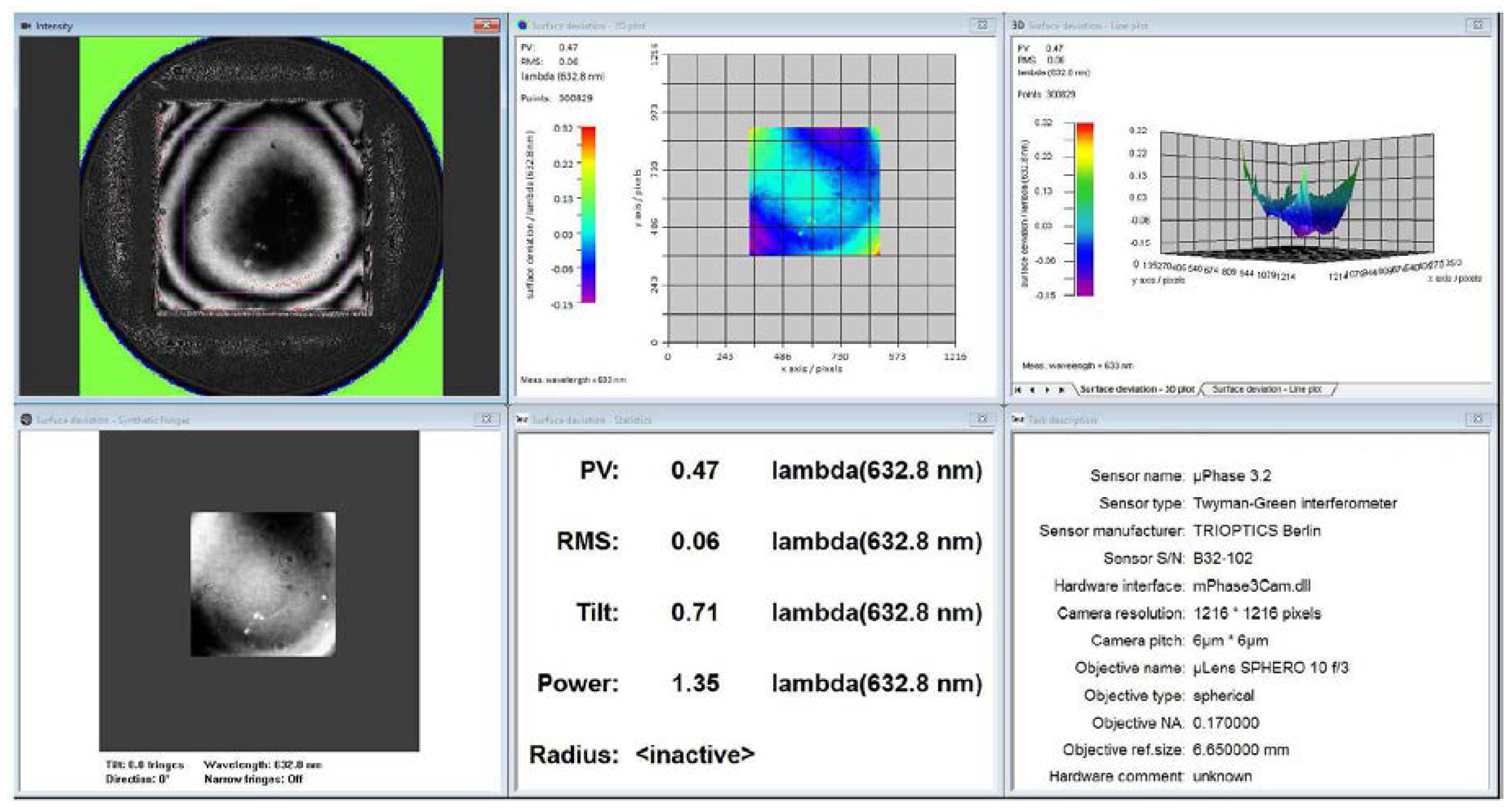
In this project, the master (32 mm × 32 mm) of a concave sphere (radius 110.2 mm) with a blazed grating (1175 grooves/mm) and an active area of approx. 24 mm × 24 mm was replicated in nickel as a thick and massive plate. This first cast (= father) could have been applied as a tool insert because of its invers geometry of the master, but since the master is destroyed after electroplating, the father was copied again into a second nickel cast (= mother) which was replicated once more into a third copy (= son) that was used as the tool inserts. With this approach, several copies of the father and mother are accessible. Due to the tool design, the son had to have a thickness of over 6 mm increasing the deposition time. The surface accuracy of the nickel casts was measured by wavefront measurements (
Table 1,
Figure 1). It was observed, that the PV deviation of the surface fitting (compared to an ideal sphere of the corresponding radius) increased with every generation from below 0.5 λ (master) up to 1.0–3.1 λ (son), where λ = 632.8 nm. The deviation originated from low internal stress upon electroplating, which cannot be avoided completely. In addition, the radius became smaller with every further generation. Sometimes, it was also observed that the fitting became better in the next generation and the pattern itself could get better after some copies. The shape of the misfit of an electroplated cast was always a saddle (
Figure 1, top right).
The moulding tool was conceived as an injection compression tool, because of the very high demands on the surface accuracy. The planned compression mode was also one reason for the thick and massive nickel inserts because the required pressures were expected to be very high. To ensure sufficient casting of the nanostructures, a heat channel was implemented to keep the material as long as possible at high temperature. To make sure that no liquid polymer is pushed back into the reciprocating screw upon compression the heat channel was equipped with a needle closure nozzle.
The process was simulated prior to tool construction by Autodesk Moldflow® analysis to confirm the injection moulding process and the aimed accuracy within the active area. The simulation predicted no shrink marks within the active area.
The injection moulding was carried out with polycarbonate types of low viscosity and good demoulding properties on an Arburg Allrounder 370 s injection moulding machine.
First production tests with a tool insert fitting of 3.1 λ resulted in moulds of a fitting deviation (PV) of average 6.5 λ and a radius of 108.3 mm. Surprisingly, changes of the compression pressures within a certain range had only small influence on the fitting but larger (= better fitting) radii were obtained at higher pressures. However, too high pressures and too long compression time resulted in demoulding problems and a demoulding spray could not be used because it filled up the grating preventing its complete casting. Additionally, at too high pressures a faster wearing of the inserts is likely.
Finally, coating of the plastic moulds with bare aluminium resulted in ready-to-use concave gratings. The metallisation revealed that the surface of the moulds was imperfect, appearing as cloudy shadows and enhancing the scattered light. These defects originated from the nickel insert, which was negatively affected by the required machining of the raw electroplated cast. This was also confirmed by microscope images before and after machining (
Figure 2).
Nevertheless, the plastic grating on the concave surface still had the capability to split white light into its spectral band confirming the replication and function of the grating (
Figure 3).
4. Conclusions
This process chain and its results reveal that even large shaped surfaces with nanostructures can be replicated precisely into a nickel cast by electroplating. Such a cast of several mm thickness was further successfully transferred into an injection compression moulding tool with which applicable moulds could be produced under mass-production conditions. Sufficient protection of the nickel cast upon further machining will reduce the surface defects of the insert and therefore of the final moulds. Additionally, it is likely that inserts with a better fitting should further enhance the fitting accuracy of the final moulds.
The now accessible polymer-gratings are an economic alternative to extensively produced glass based optical components and, to our knowledge, such an accuracy in injection moulding has not been reported yet on such large and structured areas.


