Proceeding Paper

Thermoelectric Microsensor Based on Ultrathin Si Films †

by
Gustavo Gonçalves Dalkiranis
1,*,
Pablo Ferrando-Villalba
1,‡,
Aitor Lopeandía-Fernández
1,
Llibertat Abad-Muñoz
2 and
Javier Rodriguez-Viejo
1
1
Grup de Nanomaterials i Microsistemes, Departament de Física, Universitat Autònoma de Barcelona, Bellaterra, 08193 Barcelona, Spain
2
Instituto de Microelectrónica de Barcelona—Centre Nacional de Microelectrònica, Campus UAB, Bellaterra, 08193 Barcelona, Spain
*
Author to whom correspondence should be addressed.
Presented at the Eurosensors 2018 Conference, Graz, Austria, 9–12 September 2018.
Present address: IMEC, Kapeldreef 75, 3001 Leuven, Belgium
Proceedings 2018, 2(13), 1517; https://doi.org/10.3390/proceedings2131517
Published: 7 December 2018
(This article belongs to the Proceedings of EUROSENSORS 2018)

Abstract

:
We show the use as a thermal photosensor of a thermoelectric (TE) microsensor based on ultrathin suspended Si films. The reduced thickness of the structural films enhances the extremely large thermal insulation of the sensing area (~43 µW/K), since phonons scatter in the surfaces, and guarantees a reduced thermal mass (in the µJ/K range). The sensitivity of the device is evaluated by heating with an argon laser (λ = 457 nm) in the range 0–10 mW, reaching sensitivities of around 6 × 10⁸ V/(W·m2) in high vacuum conditions and 5 × 10⁷ V/(W·m2) in environments of air at atmospheric pressure. Open circuit voltage measurements with and without light illumination with a 406 nm diode laser operating at 4 mW were conducted at temperature differences up to 50 K between the central hot region and the Si frame. The slight decrease of the Seebeck coefficient is related to the increase of carriers by photogeneration.

1. Introduction

Photosensors are sensors able to detect light (electromagnetic waves). Depending on the desired spectral sensitivity different physical principles should be considered. Between sensors using semiconductors as active materials we can highlight those directly working from:
(i)
photoelectric or photovoltaic effects, when the photons have energies over the semiconductor band gap.
(ii)
thermal-based absorption sensors when the photon energies require the generation of mid- gap states providing energy to the phonon bath.
Among the wide family of thermal absorption photosensors those based on the TE principle do not require an external current or voltage source, and therefore may offer extremely low energy detection limits depending on designs. The simplicity of that type of devices enables their miniaturization, a key factor to improving the sensitivity since it permits to reduce the heat capacity and addenda the thermal isolation of the sensing/absorbing regions. In this work, we present a microsensor made from a SOI wafer where a central silicon free-standing membrane (0.25 mm2 area) hangs from a bulk silicon frame through 40 thermoelectric silicon legs (20 doped with B and 20 doped with P) [1].

2. Materials and Methods
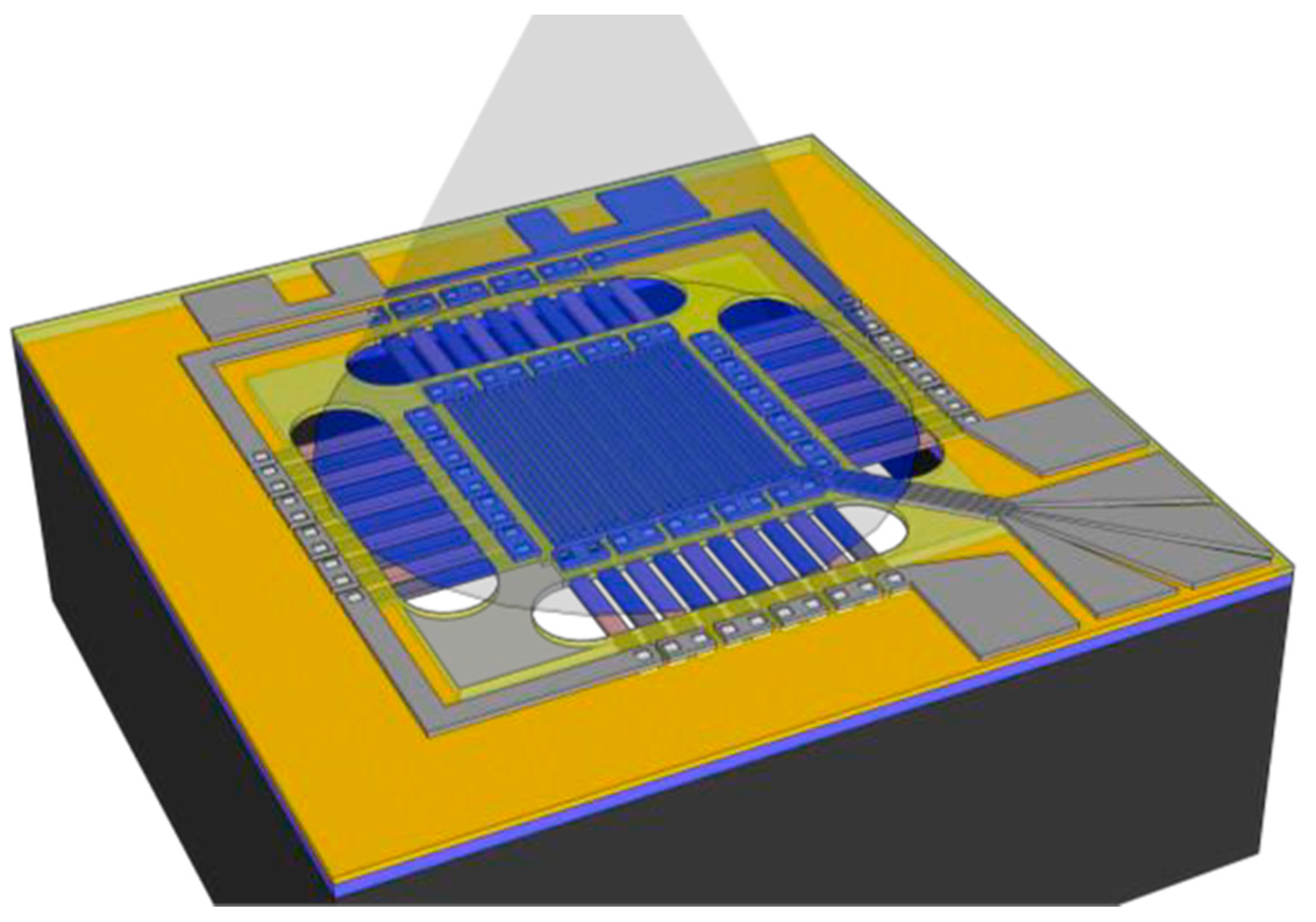
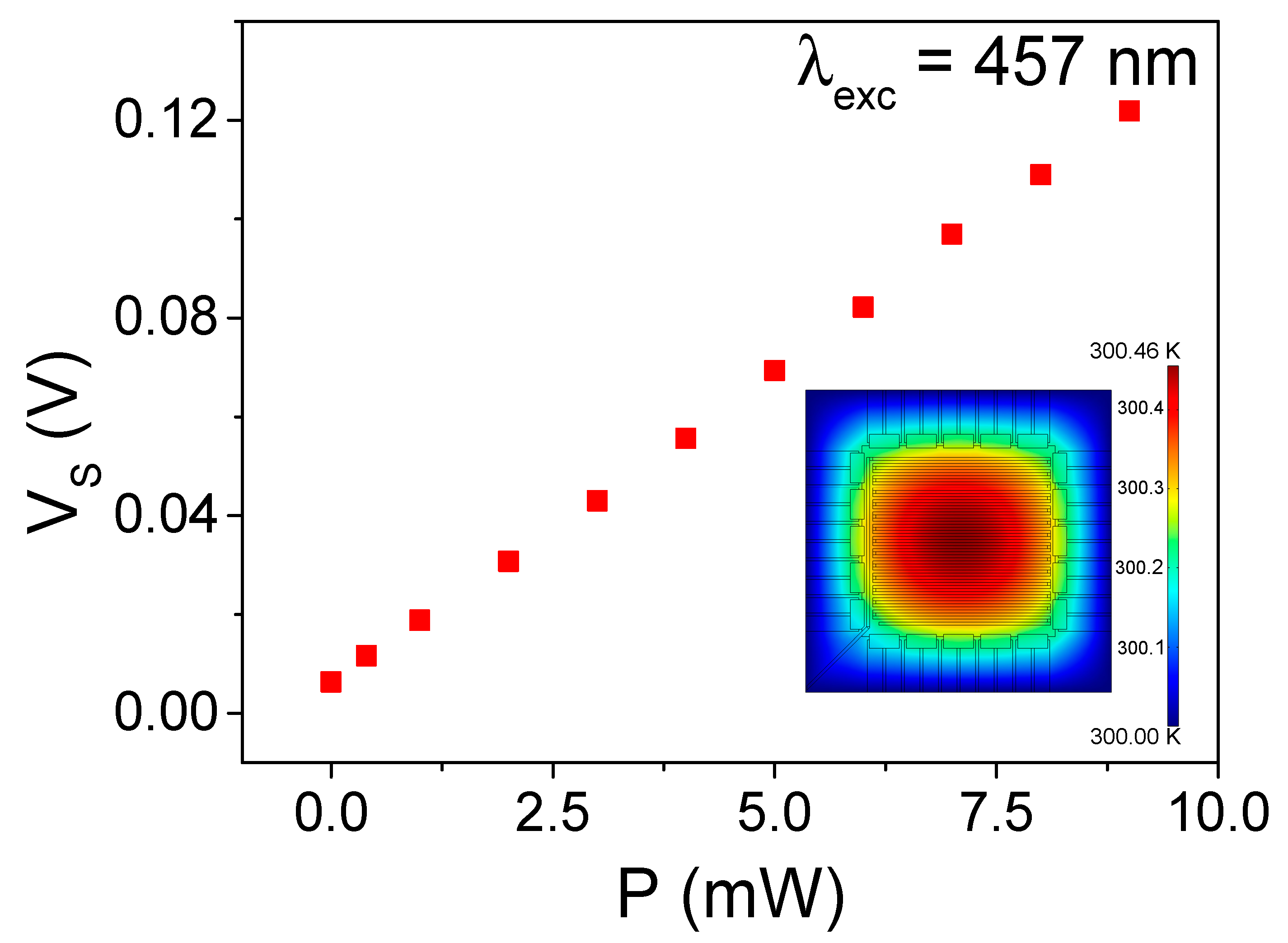
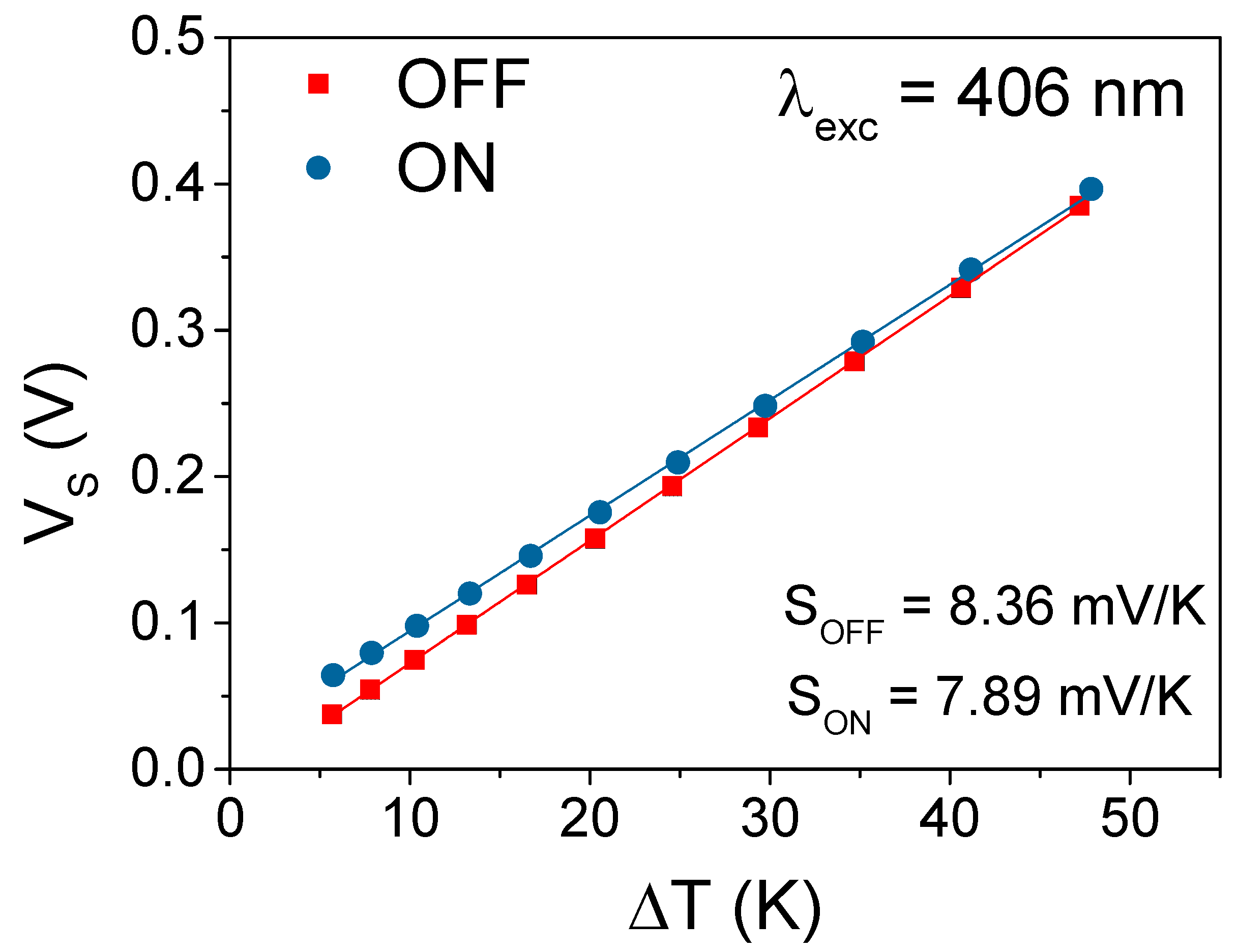
The device is equipped with electrical actuators to permit a full thermoelectric characterization, see the schematics in Figure 1. Injecting power in the central heater, temperature gradients are imposed and, in parallel, the electrical properties of the thermoelectric legs can be evaluated. The measurements show a reduction in the thermal conductivity of the Si legs from the characteristic values of 150 W/mK for bulk silicon at room temperature down to 60 W/mK, motivated by the phonon scattering at surfaces/interfaces. On the contrary, the Seebeck coefficient remains close to expected values for a Si bulk with similar doping levels (~5 × 10¹⁹ at/cm3). Finite elements modeling (FEM) is required to consider the non-flat temperature profiles of the membrane during characterization experiments. The membrane-based configuration of the device permit to guarantee a reduced thermal mass (~µJ) for sensing areas in the square millimeter range, resulting ideal as thermal photosensor. In the resulting device, the thermal sensing part of 0.25 mm2 is weakly linked with the supporting Si frame only by a conductance of 52 µW/K.
We performed measurements of the optical sensitivity to light absorption by illuminating the membrane with an Ar + laser (λ = 457 nm) at different powers up to 10 mW in ambient condition. The expected absorbance of the central multilayer stack (non-optimized) membrane is around 40% (46%) at λ = 457 nm (λ = 406 nm). In addition, we carried out open voltage circuit measurements in vacuum with and without illumination by using a 406 nm laser diode of 4 mW. To heat only the central zone the laser beam was collimated by an objective lens, as shown in Figure 1.
Figure 1. Schematic of the device showing the illuminated area.
Proceedings 02 01517 g001

3. Results

Figure 2 shows the voltage generated in the TE legs as a function of the laser power. The linear increase of the Seebeck voltage is due to the temperature difference induced by the laser beam between the central region and the silicon frame. The sensitivity of the TE sensor determined by the slope in Figure 2 amounts to 13 V/W and considering the small area of the device to an outstanding value of 5 × 10⁷ V/Wm2 in air.
Figure 3 shows the variation of the Seebeck voltage at open circuit as a function of the temperature difference between the thermoelectric legs both under illumination with the 406 nm diode laser and in dark conditions. The temperature difference was imposed by Joule heating in the central region (see Figure 1). The incident light induces a temperature rise of ~5.7 K that produces a generated voltage of 27 mV as seen by the offset of the blue line in Figure 3. This contribution decreases as the temperature gradient increases in agreement with a mechanism in which photogenerated carrier contribute to increase the electrical conductivity at the expense of reducing the Seebeck coefficient. The small change in the Seebeck coefficient from 201 µV/K to 197 µV/K does not significantly modify the sensitivity of the device enabling its use as thermal detector in a broad range of wavelength radiation.

4. Conclusions

We have designed and microfabricated a thermoelectric microsensor based on Si ultrathin film. By decreasing the thickness, the thermal conductance and heat capacity were highly reduced improving substantially the thermal insulation of the membrane. The result is a dramatic enhancement of the sensitivity of the TE device to very small temperature differences, that is to detect low-power light sources. The linear dependence of the output voltage with the input power easies the use of the microsensor as a photosensor. The measurements performed at fixed power and variable temperature differences demonstrate the slight reduction of the Seebeck coefficient as results of the photogeneration of electrical carriers.

Author Contributions

G.G.D. performed all measurements and contributed to the design of the experiments. P.F.-V. designed the simulations and corrections by FEM. A.L.-F. and L.A.-M. contributed in the designed and in the microfabrication of the device. J.R.-V. and A.L.-F. contributed to the design of the experiments. All authors participated in the writing and in the discussion of the results.

Acknowledgments

This work was supported by the Spanish Ministry of Economy and Competitiveness and the European Regional Development Fund through projects FIS2013-50304-EXP, MAT2016-79579-R, TEC2015-67462-C2-1-R and RyC-2013-12640. This work has made use of the Spanish ICTS Network MICRONANOFABS partially supported by Spanish Ministry of Economy and Competitiveness. P.F.-V. was in receipt of a FPU grant from the Spanish Ministry of Education, Culture and Sport. G.G.D. acknowledges the Brazilian National Council for Scientific and Technological Development (CNPq) his doctoral fellowship of SwB.

Conflicts of Interest

The authors declare no conflict of interest.

References

  1. Peréz-Marin, A.P.; Lopeandía, A.F.; Abad, Ll.; Ferrando-Villaba, P.; Garcia, G.; Lopez, A.M.; Muñoz-Pascual, F.X.; Rodríguez-Viejo, J. Micropower thermoelectric generator from thin Si membranes. Nano Energy 2014, 4, 73–80. [Google Scholar] [CrossRef]
Figure 2. Plot of the voltage at open circuit as a function of laser power. The inset plot shows the temperature profiles simulated by FEM.
Proceedings 02 01517 g002
Figure 3. Plot of the Seebeck voltage at open circuit as a function as a function of temperature difference. When the device is illuminated and without light.
Proceedings 02 01517 g003
Publisher’s Note: MDPI stays neutral with regard to jurisdictional claims in published maps and institutional affiliations.

