Proceeding Paper

Transfer Printing Technology for Fabricating Chemical Sensors Based on Tin Dioxide Nanowires †

by
Florentyna Sosada-Ludwikowska
*,
Robert Wimmer-Teubenbacher
and
Anton Köck
Microelectronics, Materials Center Leoben Forschung GmbH, 8700 Leoben, Austria
*
Author to whom correspondence should be addressed.
Presented at the Eurosensors 2018 Conference, Graz, Austria, 9–12 September 2018.
Proceedings 2018, 2(13), 1076; https://doi.org/10.3390/proceedings2131076
Published: 21 November 2018
(This article belongs to the Proceedings of EUROSENSORS 2018)

Abstract

:
Multi-nanowire based chemical gas sensors were produced employing a fast and simple transfer printing technology. SnO2 nanowires (NWs) were grown by a specific two-step technology including spray pyrolysis deposition and a thermal annealing process in presence of a Cu-catalyst. Subsequently the SnO2 NWs were print transferred by a polydimethylsiloxane (PDMS) stamp on Si-substrates with gold inter-digital electrode structures (IDES) creating a multi-NW chemical sensing device. The print-transfer technology enables a fast, easy and cheap fabrication of NW-based sensor devices with a good reproducibility. High sensitivity to H2S has been achieved, the performance results are presented in this work.

1. Introduction

Air quality control is a major issue in today’s world due to air pollution caused by often odorless harmful or even toxic gases [1,2]. Monitoring of potentially harmful gases can be performed by conductometric chemical sensor devices. This type of gas sensor provides ease of use because the response to a specific gas is simply measured by a change of the electrical resistance. The most prominent group of materials used for chemical gas sensors are metal oxides due to their high sensitivity to a large number of gases. Moreover, this type of sensors can be fabricated at relatively low costs due to easy and flexible production. A most suitable approach to optimize the sensor performance are metal oxide NWs because they exhibit a high surface area [3]. A wide range of production methods is known from literature—but the missing link between nanowire fabrication and functional gas sensors is the implementation of those nanomaterials on proper electronic structures. One of the methods is the transfer printing technology which enables a fast, reproducible and cost-effective method to integrate nanowires on gas sensing devices [4].

2. Production of SnO2 NWs

A specific two-step synthesis was used for SnO2 NWs fabrication [5]. First a thin (400 nm) layer of SnO2 was deposited on Si by spray pyrolysis technology. Secondly a Si-substrate was sputtered with a thin (40 nm) Cu-layer; subsequently both coated samples were placed in a tube furnace “face-to-face” with a distance in between them of 2–5 mm. An annealing process in Ar-atmosphere at a temperature of 900 °C for 3 h resulted in growth of SnO2 NWs, which have 50–200 nm in diameter and 10–100 μm in length.

3. Transfer Printing Process

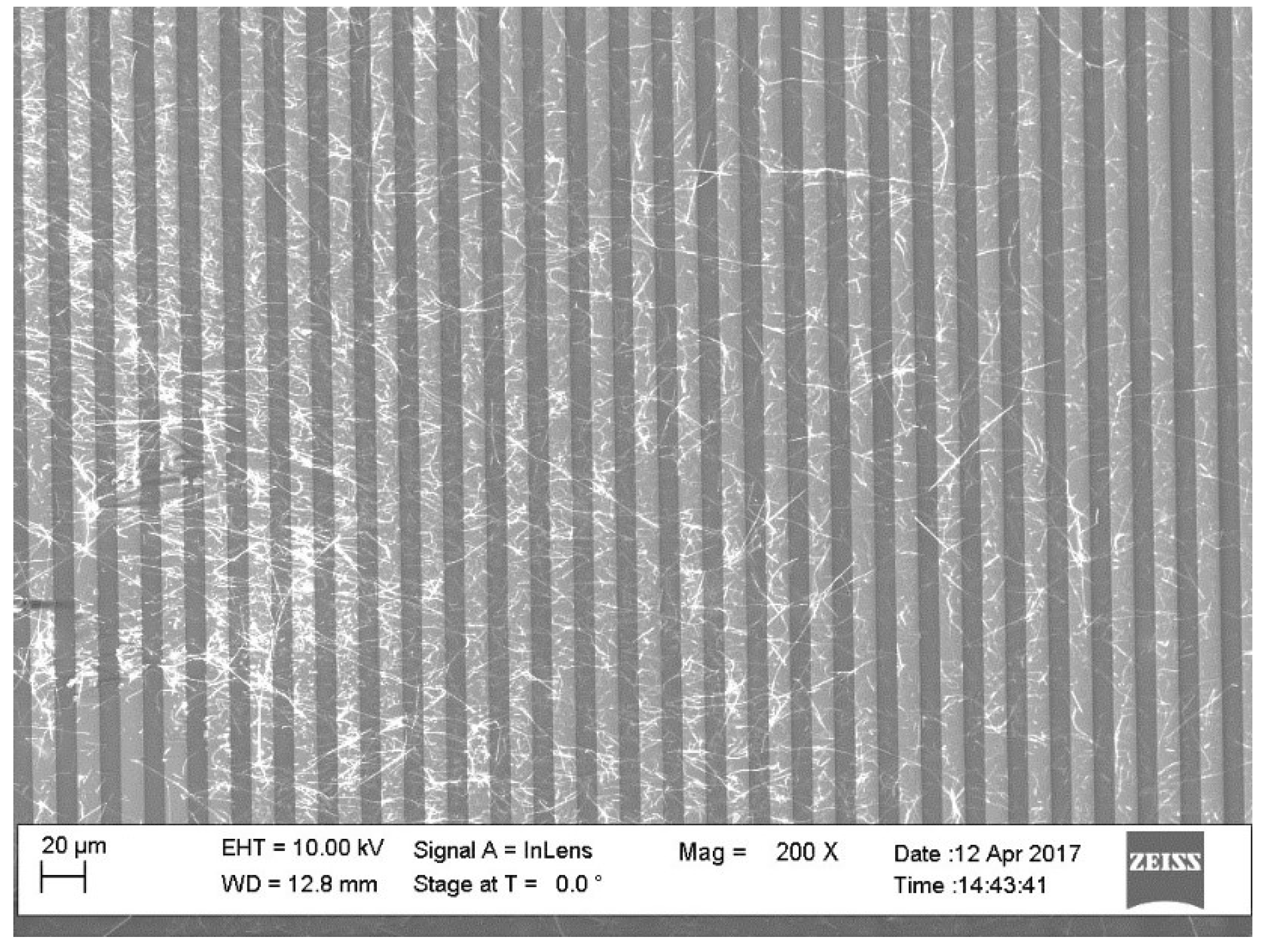
The implementation of SnO2 NWs on gas sensing devices was performed by a “dry” transfer printing technology. In contrast to “wet” processes, where NWs are harvested in organic solutions and implemented on the devices by i.e., spin coating, a “dry” process avoids potential contamination of the gas sensitive material by organic residuals, which might be detrimental for the sensor performance. A planar polydimethylsiloxane (PDMS) stamp 5 × 5 mm was fabricated by standard Dow Corning Sylgard 184 10:1 recipe. The transfer process was performed by pressing the PDMS stamp to the SnO2 NWs substrate to harvest the NWs, and then pressing the stamp with the NWs to the gas sensing substrate to deposit the NWs. In this work two gas sensing substrates were used: an Au-IDES (Inter-Digital Electrode) structure on a SiO2 coated Si-substrate, and a membrane-based micro-hotplate device from ams AG in order to demonstrate the suitability of the transfer printing technology for NW implementation on real devices. The first one was prepared by photolithography, evaporation (5 nm Ti, 200 nm Au) and lift-off; electrodes width and the distance between electrode fingers are 10 µm. The Au-IDES based sensors (size: 5 × 10 mm) were glued on micro heaters (10 × 2 Pt 6.8 Delta-R GmbH, Mannheim, Germany) and thermocouple (4 × 1 Pt100, Delta-R GmbH, Mannheim, Germany) with ceramabond (Aremco Products, Inc., distributor in Hannover Germany)— see Figure 1. Next, the SnO2 NWs were print transferred on the electrode structure (see Figure 2), then the samples were bonded and the gas sensitivity to H2S was measured. On the second membrane-based micro-hotplate device the SnO2 NWs were successfully transferred on the IDES structure without damaging the membrane. 2-point measurements were performed to proof functionality of the devices and check the resistance change of the NWs by heating the sample.

4. Gas Sensing Performance

Gas sensing measurements were performed by an automated gas measurement setup. The background gas was synthetic air (80% N2, 20% O2) and the flow rate was kept constant at 1000 sccm. Gas concentrations of H2S were varied between 10, 100 and 1000 ppb in different relative humidity (r.h.) levels: 25%, 50% and 75%. A constant current of 10 nA was used to measure the resistivity of the SnO2-NWs, the sensors were operated at 400 °C for all gas sensing experiments. Sensitivity was calculated as follows:
S = R a i r R g a s R a i r
Two Si-based sensors (sensor A and B) were produced by the same NW transfer printing method, the resulting sensitivities are shown on Figure 3a,b. Sensor A has a slightly higher sensitivity than sensor B, both sensors show a similar behavior, which indicates that the printing transfer process is reproducible. Sensitivities for both sensors are highest for 25% r.h. which indicates cross-sensitivity to humidity. Very good response was achieved for H2S concentration as low as 10 ppb—Figure 3c shows the sensitivity of sensor B measured 4 months after the first measurements—the sensitivity has slightly increased most probably due to the storage in humid atmosphere and a resulting higher number of oxygen species on the surface of the SnO2 NWs.

5. Electrical 2-Point Measurements of Membrane-Based Structures

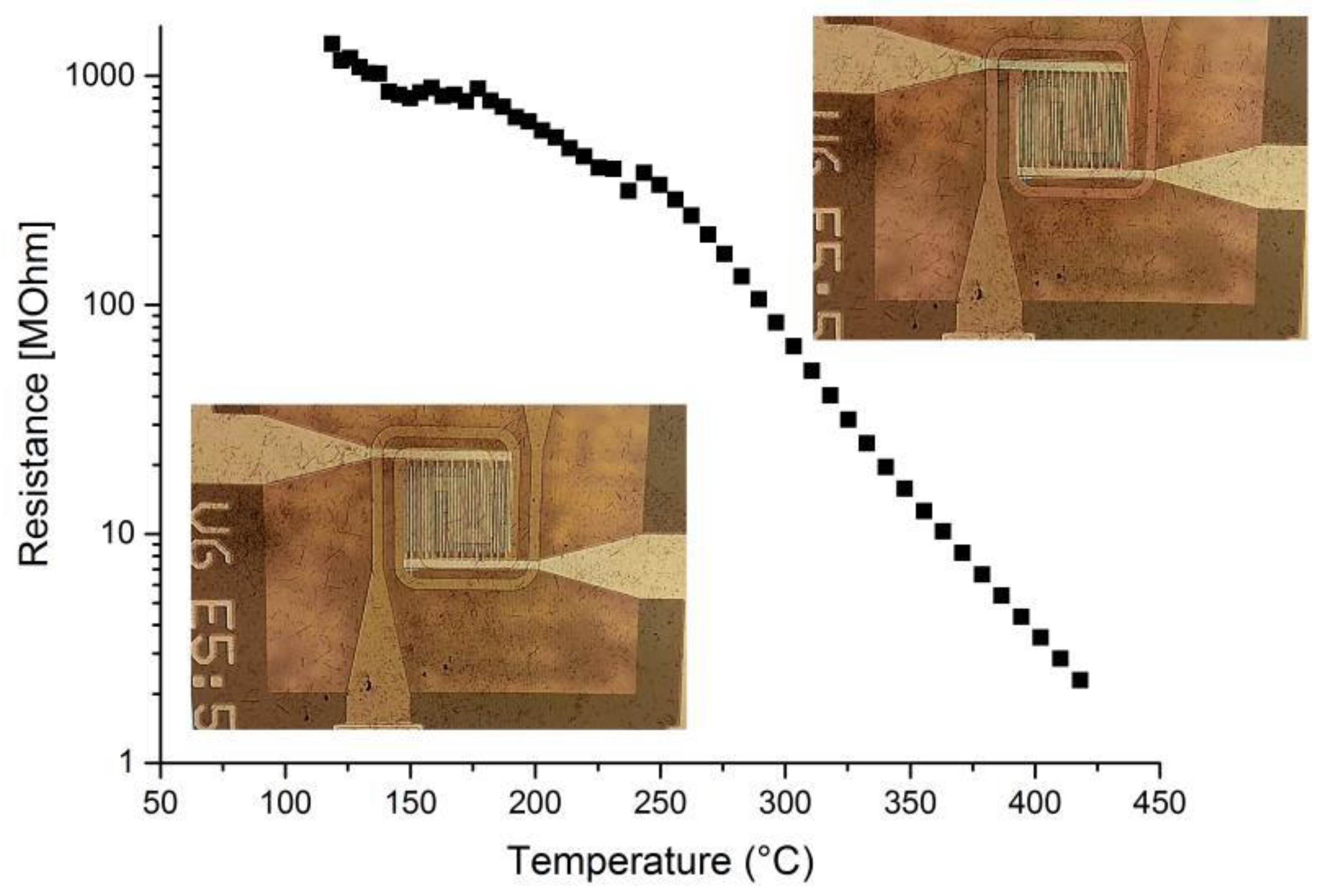
By applying different currents, the micro heater was set to the desired operation temperature. 2-point measurements (Kleindiek PS4) were performed on the membrane-based micro-hotplate device by placing two needles on the electrodes, a constant current of 1 nA was applied to the NWs. The change of voltage was measured and the resistance was calculated (Figure 4). The SnO2-NWs are obviously connecting the IDES electrodes, the resistance decreases with increasing temperature—which is a typical behavior of SnO2. The gas sensing performance measurements of the structures are currently in progress.

6. Conclusions

In this work SnO2-NW based sensor devices were fabricated by a simple print transfer technology. Reproducible multi-NWs gas sensing devices have been realized by this technology, a high sensitivity for low concentrations of H2S has been achieved. We have successfully demonstrated that this technology can be also employed to integrate NWs on membrane-based micro-hotplate devices without damaging the structure, which is of high importance for fabrication of real devices. Use of the dry print transfer technology for integration of SnO2-NWs on CMOS based micro-hotplate chips is in progress.

Author Contributions

F.S. performed the experiments; F.S and A.K. analyzed the data; R.W. contributed materials; F.S. and A.K. wrote the paper.

Acknowledgments

This work was performed within the projects “FunkyNano—Optimized Functionalization of Nanosensors for Gas Detection by Screening of Hybrid Nanoparticles” funded by the FFG—Austrian Research Promotion Agency (Project No. 858637) and “MSP—Multi Sensor Platform for Smart Building Management” funded by the European Commission (FP7-ICT-2013-10 Collaborative Project No. 611887).

References

  1. Sun, Y.-F.; Liu, S.-B.; Meng, F.-L.; Liu, J.-Y.; Jin, Z.; Kong, L.-T.; Liu, J.-H. Metal Oxide Nanostructures and Their Gas Sensing Properties: A Review. Sensors 2012, 12, 2610–2631. [Google Scholar] [CrossRef] [PubMed]
  2. Air Quality Deteriorating in Many of the World’s Cities. 7 May 2014. Available online: http://www.who.int/mediacentre/news/releases/2014/air-quality/en/ (accessed on 17 July 2018).
  3. Ponzoni, A.; Baratto, C.; Cattabiani, N.; Falasconi, M.; Galstyan, V.; Nunez-Carmona, E.; Rigoni, F.; Sberveglieri, V.; Zambotti, G.; Zappa, D. Metal oxide gas sensors, a survey of selectivity issues addressed at the SENSOR Lab, Brescia (Italy). Sensors 2017, 17, 714. [Google Scholar] [CrossRef] [PubMed]
  4. McAlpine, M.C.; Ahmad, H.; Wang, D.; Heath, J.R. Highly ordered nanowire arrays on plastic substrates for ultrasensitive flexible chemical sensors. Nat. Mater. 2007, 6, 379. [Google Scholar] [CrossRef] [PubMed]
  5. Köck, A.; Tischner, A.; Maier, T.; Kast, M.; Edtmaier, C.; Gspan, C.; Kothleitner, G. Atmospheric pressure fabrication of SnO2-nanowires for highly sensitive CO and CH4 detection. Sens. Actuators B Chem. 2009, 138, 160–167. [Google Scholar] [CrossRef]
Figure 1. Scheme of Si-based gas sensing device with Au-IDES structures and external heating.
Proceedings 02 01076 g001
Figure 2. Part of the Au-IDES structure with many SnO2-NWs in parallel forming the sensing structure.
Proceedings 02 01076 g002
Figure 3. Sensitivities of SnO2 nanowires-based gas sensors ((a) sensor A; (b) sensor B)—both of them prepared by the same technology. The sensitivity of sensor B increases after 4 months of storage (c).
Proceedings 02 01076 g003
Figure 4. 2-point measurement of membrane-based gas sensor structure with transfer printed SnO2 nanowires on top of the electrodes.
Proceedings 02 01076 g004
Publisher’s Note: MDPI stays neutral with regard to jurisdictional claims in published maps and institutional affiliations.