Abstract
This paper reports a design of an exchangeable miniaturized mass spectrometry chip using spring-loaded pins and O-rings for electrical and fluidic connections. This planar microelectromechanical system (MEMS)-chip works with 300 µm high silicon structures between two borosilicate glasses and has a size of 13 mm × 7 mm. Because of its small size a small vacuum pump is sufficient, and it is suitable for mobile measurements and portable applications. Because of exchangeability of MEMS-chips with fluidic and electrical high voltage connections a direct comparison between chips is possible.
1. Introduction
In the chemical process industry, sensor systems are required for process monitoring and control, in order to achieve a safe and economical production. Mass spectrometry is an opportunity to analyze gaseous media, but current versions are bulky and work off-line. The goal of our project is to develop a miniaturized mass spectrometer for fast in-line measurements with high resolution and accuracy. Another possible application in the future is mobile analysis for fire fighters in emergency situations. The use of MEMS-chips for ion separation and detection provide a miniaturized system. Thus small vacuum pumps and small supply voltages are sufficient to run a mass spectrometer [1].
Exchangeable MEMS-chips of the presented mass spectrometer are made of silicon. Usually, these chips are glued to a circuit board, electrical connections are realized with bond wires, and glued capillary tubes are used to transport sample and plasma gas into the chip. This means, a new circuit board is necessary for every chip, and therefore, conditional of manufacturing differences of the circuit boards prevent a direct comparison of MEMS-chip-prototypes. Long-term measurements show a reduction of measureable ion current with MEMS-chips based on silicon, as well as a reaction of the glue of the capillary tubes with the plasma. In this work, a concept for exchangeable sensor chips is presented.
2. Materials and Methods
Silicon structure has a height of 300 µm and is bonded on a 13 mm × 7 mm borosilicate glass which provides a carrier. On the top of the silicon structure is borosilicate glass, too, which is structured for electrical and fluidic connections.
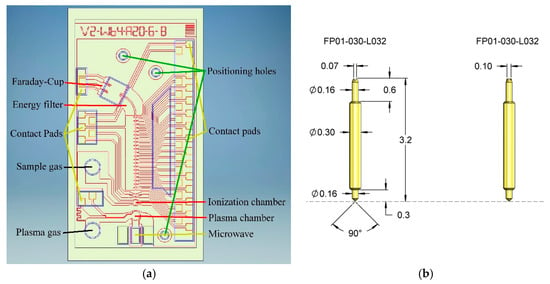
Argon is led into a plasma chamber by a hole in the top glass substrate and is ignited by a high voltage ignition spark. A microwave generator excites a micro-plasma at 2.45 GHz as an electron source for the mass spectrometer. A focused electron beam with distinct energy is used for the ionization of the sample. The ion optic to focus the ion beam into the mass separator is located directly behind the ionization chamber. Within the mass separator, the ions are separated by time variant travelling waves. A synchronous ion shield filters the ionized sample by velocity and therefore by mass. The Faraday Cup catches all ions, neutralizes them, and forwards the energy off the MEMS-chip to a low noise amplifier (Figure 1a) [2].

Figure 1.
(a) Design of exchangeable MEMS-chip; (b) dimensions of the used spring-loaded pins in mm [3].
The electrical and fluidic connections of a MEMS-chip are on the top of the silicon structures. This side is faced down to gold plated spring-loaded pins and o-rings which are located on a circuit board. Via spring-loaded pins the circuit board transmits voltage supplies, travelling wave signals and microwave to the chip. The utilised pins have a diameter of 300 µm, a height of 3.2 mm and a stroke of 500 µm (Figure 1b). A stroke is necessary to ensure electrical connections of all pins. Vias with a diameter of 350 µm are used to fix spring-loaded pins into circuit board.
Capillary tubes are passed through two holes in circuit board directed to MEMS-chip and are fixed with glue. Two chemically inert fluorine o-rings between circuit board and chip ensure a leak-proof fluidic connection.
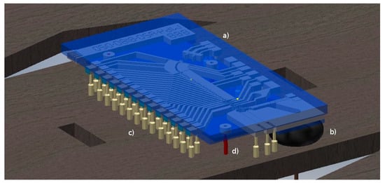
Accurate positioning and reliable electric contact of a MEMS-chip is ensured by three additional positioning pins, as shown in Figure 2d). They ensure the positioning of MEMS-chip.

Figure 2.
First concept of an exchangeable MEMS-chip (a) MEMS-Chip with a size of 13 mm × 7 mm and mass spectrometer structure; (b) Plasma gas channel is sealed with an O-ring; (c) spring-loaded pins for electric connections; (d) spring-loaded pins to ensure the positioning of MEMS-Chip.
3. Results
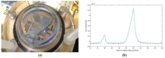
MEMS-chip was built in the system to test whole functionality. Plasma gas was led into the chip, the microwave generator was started and a high voltage ignited the plasma (Figure 3a). A measurement of a mass spectrum shows that the triggering of the chip electrodes works as expected. As in Figure 3b visible the MEMS-chips detects Argon ions, once charged (40 amu) and twice charged (20 amu). This mass spectrum is in accordance to a mass spectrum of a wire bonded MEMS-chip.

Figure 3.
(a) Mounted MEMS-chip in vacuum chamber in operation; (b) Mass spectrum with Argon as plasma and sample gas.
4. Discussing and Outlook
The exchangeable MEMS-chips are made of silicon. Other than that, mentioned reduction of measureable ion current at long-term measurements the etching process of silicon chips causes undercut and a rough surface. The next step will be the use of nickel instead of silicon. Therefore the LiGa-technology (Lithography and Electroplating) is suitable for fabrication of new MEMS-chips.
In the current version, a microscope is required to exchange the chip due to its small geometry. This can be overcome by an advanced module design, in which a MEMS-chip is mounted on a dedicated circuit board. This approach improves mechanical stability by employing more robust positioning pins. Furthermore, a memory module can be added to the replaceable circuit board, in which calibration and run-time data for each individual MEMS-chip can be stored. This approach enables chip exchange without any software modification of the system.
Author Contributions
S.W. designed the chip and wrote the paper. P.H. helped to install and align the chip an the circuit board and B.J. took the measurements and created the spectres. All authors have read and agreed to the published version of the manuscript.
Funding
This research was funded by Federal Ministry for Economic Affairs and Energy.
Conflicts of Interest
The author declares no conflict of interest. The founding sponsors had no role in the design of the study; in the collection, analyses, or interpretation of data; in the writing of the manuscript, and in the decision to publish the results.
References
- Hauschild, J.-P.; Wapelhorst, E. Mass spectra measured by a fully integrated MEMS mass spectrometer. Int. J. Mass Spectrom. 2007, 264, 53–60. [Google Scholar] [CrossRef]
- Temiz, Y.; Lovchik, R.D.; Kaigala, G.V.; Delamarche, E. Lab-on-a-chip devices: How to close and plug the lab? Microelectron. Eng. 2015, 132, 156–175. [Google Scholar] [CrossRef]
- Datasheet of FP01-030-L032. FEINMETALL GmbH. Spring-Loaded Pin. Available online: http://www.feinmetall.de/fileadmin/produkte/datenblaetter/de/FP01-030-L032_DE.pdf (accessed on 13 July 2018).
Publisher’s Note: MDPI stays neutral with regard to jurisdictional claims in published maps and institutional affiliations. |
© 2018 by the authors. Licensee MDPI, Basel, Switzerland. This article is an open access article distributed under the terms and conditions of the Creative Commons Attribution (CC BY) license (https://creativecommons.org/licenses/by/4.0/).