Proceeding Paper

Design of a Photonic Crystal Defect Waveguide Biosensor Operating in Aqueous Solutions at 1.34 µm †

1
AIT, Austrian Institute of Technology GmbH, Center for Health & Bioresources, 1210 Vienna, Austria
2
FH Campus Wien, University of Applied Sciences, 1100 Vienna, Austria
3
SUPA, School of Physics and Astronomy, University of St. Andrews, St. Andrews KY16 9SS, UK
*
Author to whom correspondence should be addressed.
Presented at the Eurosensors 2018 Conference, Graz, Austria, 9–12 September 2018.
Proceedings 2018, 2(13), 1026; https://doi.org/10.3390/proceedings2131026
Published: 14 November 2018
(This article belongs to the Proceedings of EUROSENSORS 2018)

Abstract

:
A two-dimensional photonic crystal defect waveguide sensor based on CMOS-compatible silicon-on-insulator technology was designed for operation in aqueous solutions at a wavelength of 1.34 µm, by the use of the 3D Plane Wave Expansion and the Finite Difference Time Domain simulation method. An operation under water in this wavelength regime allows for a significantly smaller propagation loss in contrast to the state-of-the-art operation wavelength of photonic crystals at 1.55 µm. The sensor working principle is label-free and based on evanescent wave sensing exploiting the local refractive index change induced by the specific binding of target molecules to a capture molecules immobilized on the surface of the phontonic crystal structure. We experimentally proved the theoretical predications of our simulations and demonstrated the sensing functionality of the photonic crystal defect waveguide using the biotin-straptavidin binding system.

1. Introduction

The label-free detection of biomolecules in liquid samples is a highly desirable feature in a wide range of applications such as medical and pharmaceutical research, molecular diagnostics, environment monitoring, as well as process and quality control in food industry. During the last decades various integrated optical waveguide concepts have been intensively investigated as a promising means to realize sensitive label-free biomolecule detection [1]. All these concepts exploit the effective refractive index change of the guided optical wave that is induced by the specific binding of target molecules to a thin biochemical functionalization layer on top of the waveguide surface. In recent years, above all silicon photonic waveguide devices have gained particular popularity in this field. The high index contrast of this material system allows for compact nanophotonic structures not possible with lower refractive index materials, which enables the integration of several sensing components on a single chip. In addition, CMOS compatibility ensures the possibility to transfer the sensor concepts to cost-effective mass production at a later stage. Moreover, the availability of compact, low-priced, and high-quality laser sources in the telecom wavelengths domains at 1.3 µm and 1.55 µm facilitates the implementation of the overall sensor system. Among the nanophotonic structures, planar photonic crystal (PhC) structures have attracted considerable attention among researchers due to their capability to provide strong light-matter interaction in a tiny area by the appearance of so called slow light modes [2,3].
In this paper, we report the design of a 2D silicon PhC defect waveguide operating at 1.34 µm and demonstrate its suitability for biosensing by observing the binding of single and multi-layer biotin-streptavidin biofilms. With respect to the choice of operation wavelength, propagation loss represents a very important issue because it directly impacts the overall sensing performance. Considering this aspect, the 1.34 µm wavelength region is clearly advantageous over the 1.55 µm wavelength region due to the significantly lower absorption in water (see Figure 1a). Surprisingly, to the best of our knowledge, so far all PhC defect waveguides for biosensing applications described in literature have been designed for wavelengths in the 1.55 µm region.

2. Sensor Concept and Photonic Crystal Defect Waveguide Design

The PhC defect waveguide devices were fabricated on silicon-on-insulator wafers with 220 nm monocrystalline silicon layer and a 2 µm thick buried oxide employing electron beam lithography and reactive ion etching. After definition of the waveguide structures, the PhC membrane was under etched using HF. Figure 1b shows a scanning electron microscope picture of the fabricated PhC defect waveguide, which had an overall length of about 90 µm.
Achieving efficient coupling between a conventional wire waveguide mode and a slow light mode in a PhC defect waveguide represents a challenging task in the design because a direct transition results in high losses. The major cause for these losses is the impedance mismatch between the conventional and PhC defect waveguide modes. For PhC defect waveguides operated in air it has already been shown that a few micron long intersection with a PhC defect waveguide supporting a faster mode can significantly enhance the coupling efficiency between the conventional waveguide mode and the slow light mode in the PhC defect waveguide [4,5]. By modifying the lattice periods and the hole diameters of this intersection PhC defect waveguide the group velocities can be adapted such that the coupling losses are reduced significantly. The input intersection area with an overall length of about 5 µm is displayed as a red dashed rectangle in Figure 1b. Therefore we performed 2D Finite Difference Time Method (FDTD) simulations employing an effective index approach for the optimization of the coupling efficiencies between the conventional and PhC defect waveguides. In the intersection, the period along the defect direction was reduced in 10 nm steps from 450 nm down to 410 nm.
The PhC defect waveguide parameters were determined by the use of a 3D Plane Wave Expansion (PWE) simulation method [6] for calculating the PhC band structures and the defect modes. The defect waveguide was defined by one row of holes along the Γ-K with a radius rd which was smaller than radius r of the holes of the PhC. The radius r1 of the first row next to the defect line was also slightly smaller (r1 = 140 nm) than that of the other PhC holes. After an iterative optimization procedure of the photonic crystal parameters, a period length of a = 410 nm, a hole radius of r = 165 nm and a defect hole radius of rd = 100 nm were computed.
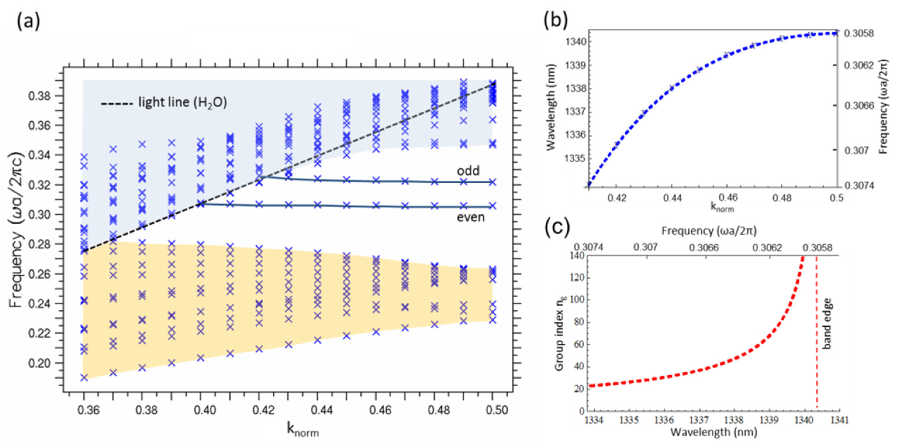
In the planar 2D photonic crystal defect waveguides, the backscattering mechanism of light at each unit cell and the omnidirectional reflection are leading to the formation of slow light modes with a remarkably low group velocity. The use of the slow light mechanism in photonic crystal biosensors offers the possibility for spatial compression of optical energy, which leads to a significant enhancement of the interaction between light and the biosensitive layer by up to a factor of >50. Figure 2a,b displays the simulation results of the band structures and the even and odd defect modes of the photonic crystal sensor device. In Figure 2c the calculated group index ng which is equivalent to the slow light factor is plotted as a function of frequency. The group index and therefore the slow light factor strongly increase by approaching to the Briouline zone edge (BZE). Compared with conventional photonic devices with a typical sensing arm length of several millimeters the use of photonic crystals allows a significant reduction of the sensing length, and thus PhCs can be exploited for the development of very compact photonic sensors.

3. Measurements and Results

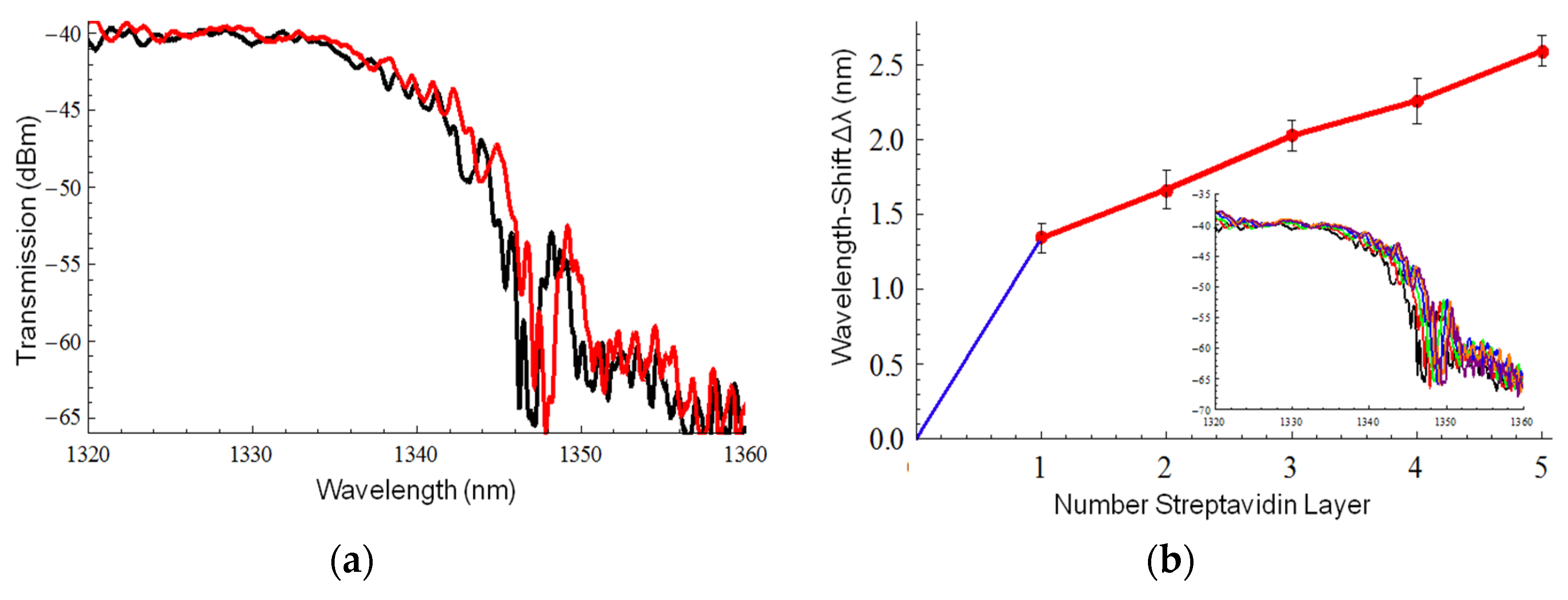
The PhC sensors were chemically modified with iminobiotin to enable reversible measurements of the protein streptavidin. The modification steps included cleaning, activation, silanization, thiol-ene click coupling, covalent attachment of polyethyleneimine and iminobitinylation [7]. Five STA/IB-PEI layer-stacks were deposited on a BSA blocked iminobotinylated PhC sensor, and then regenerated by rinising with 3.5 mM HCl. Optical characterization of the PhC waveguide components and biosensing experiments were carried out on a fully automatized setup in an end-face coupling configuration employing piezoelectric alignment stages at the input and output. The TE polarized light was coupling in the feeding waveguide via a polarization maintaining conical lensed optical fiber. At the output another lensed fiber was used to collect the light. Figure 3a displays the transmission spectra of the BSA blocked, iminobiotinylated photonic crystal sensor (black curve) and the photonic crystal sensor with a single STA/IB-PEI layer-stack (red curve). In the measured transmission spectrum of the photonic crystal structure, the band edge was observed around 1346 nm, which matches very well with the design value. The small deviation of about 6 nm of the band gap wavelength between the simulated and measured results can be explained by very small deviation of the fabricated device from the optimized design values. Figure 3b plots the wavelength shift of the transmission spectrum observed after each STA/IB-PEI layer-stack deposition (red curve) with respect to the spectrum of the non-functionalized PhC sensor. The inset shows the corresponding spectra. Wavelength shifts of about 1.4 nm for the single STA/IB-PEI layer-stack and 2.6 nm for the stacked five STA/IB-PEI layer-stacks of the transmission spectra were measured.

4. Conclusions

In this study, for the first time, to best of our knowledge a two-dimensional photonic crystal defect waveguide biosensor based on CMOS-compatible silicon-on-insulator technology was designed for operation in aqueous solutions at a wavelength of 1.34 µm. An operation in this wavelength regime bears a significantly smaller propagation loss in contrast to the state of the art operation wavelength 1.55 µm of photonic crystals. We demonstrated the sensor working principle where the spectral transmission characteristics of the sensor was measured with TE- polarized light for single layer and stacked five bio layer system.

Author Contributions

M.W. and R.H. performed all simulations and designed the PhC sensor; E.M. performed the biochemical functionalization; E.M. and P.M. performed the experiments; L.O. fabricated the PhC sensor; M.W., E.M. and R.H. analyzed the data; all authors contributed to writing the manuscript. All authors have read and agreed to the published version of the manuscript.

Acknowledgments

This work was supported by the Austrian NANO Initiative under the grant PLATON Si-N (project No. 1103). The work of Markus Wellenzohn was supported by the MA 23 (FH-Call 16) under the project “Photonik-Stiftungsprofessur für Lehre”.

Conflicts of Interest

The authors declare no conflict of interest.

References

  1. Estevez, M.C.; Lechuga, L.M. Integrated optical devices for lab-on-a-chip biosensing applications. Laser Photonics Rev. 2011, 6, 463–487. [Google Scholar] [CrossRef]
  2. Krauss, T.F. Slow light in photonic crystal waveguides. J. Phys. D Appl. Phys. 2006, 40, 2666–2670. [Google Scholar] [CrossRef]
  3. Baba, T. Slow light in photonic crystals. Nat. Photonics 2008, 2, 465–473. [Google Scholar] [CrossRef]
  4. Barnier, D.; Cassan, E.; Le Roux, X.; Marris-Morini, D.; Vivien, L. Efficient band-edge light injection in two –dimensional planar photonic crystals using a gradual interface. Opt. Eng. 2009, 48, 070501-1–070501-3. [Google Scholar] [CrossRef]
  5. Hugonin, J.P.; Lalanne, P.; White, T.P.; Krauss, T.F. Coupling into slow-mode photonic crystal waveguides. Opt. Lett. 2007, 32, 2638–2640. [Google Scholar] [CrossRef] [PubMed]
  6. Available online: https://www.synopsys.com/optical-solutions/rsoft/passive-device-bandsolve.html (accessed on 13 November 2018).
  7. Melnik, E.; Muellner, P.; Bethge, O.; Bertagnolli, E.; Hainberger, R.; Laemmerhofer, M. Streptavidin binding as a model to characterize thiol–ene chemistry-based polyamine surfaces for reversible photonic protein biosensing. Chem. Commun. 2014, 50, 2424–2427. [Google Scholar] [CrossRef]
Figure 1. (a) Propagation losses of light in water as a function of wavelength; (b) Scanning electron microscope picture of the fabricated photonic crystal defect waveguide with the input intersection area (dashed rectangle). To minimize radiation losses an input intersection area was included into the PhC device where different period lengths (ai) were used.
Proceedings 02 01026 g001
Figure 2. (a) 3D plane wave expansion method simulation results of band diagram as well as the corresponding defect mode below the light line for TE-polarized light; (b) dispersion characteristic of the defect mode (even); (c) calculated group index as function of the frequency for the defect mode (even).
Proceedings 02 01026 g002
Figure 3. (a) Measured transmission spectra (with TE-polarized light) of the photonic crystal sensor device without bio-functioalization (black curve) and with a single bio-functionalized layer (red curve); (b) Spectral shift of the PhC biosensor as function of the number of STA/IB-PEI layer-stacks with respect to the non-functionalized PhC sensor.
Proceedings 02 01026 g003
Publisher’s Note: MDPI stays neutral with regard to jurisdictional claims in published maps and institutional affiliations.