Proceeding Paper

Tailoring Active Defect Centers During the Growth of Group IV Crystals †

by
Michele Cascio
1,2,‡,
Ioannis Deretzis
1,‡,
Giuseppe Fisicaro
1,‡,
Giuseppe Falci
1,2,‡,
Giovanni Mannino
1,‡ and
Antonino La Magna
1,*,‡
1
Consiglio Nazionale delle Ricerche, Istituto per la Microelettronica e Microsistemi, Zona Industriale VIII Strada 5, I95121 Catania, Italy
2
Department of Physics and Astronomy and INFN, University of Catania, Via S. Sofia 64, 95125 Catania, Italy
*
Author to whom correspondence should be addressed.
Presented at the 11th Italian Quantum Information Science conference (IQIS2018), Catania, Italy, 17–20 September 2018.
These authors contributed equally to this work.
Proceedings 2019, 12(1), 32; https://doi.org/10.3390/proceedings2019012032
Published: 19 December 2019
(This article belongs to the Proceedings of 11th Italian Quantum Information Science conference (IQIS2018))

Abstract

:
Defects, e.g., Vacancies (Vs) and Defect-impurity centers, e.g., Nitrogen-Vacancy complexes (NVs), in group IV materials (diamond, SiC, graphene) are unique systems for Quantum Technologies (QT). The control of their positioning is a key issue for any realistic QT application and their tailored inclusion during controlled crystal-growth processes could overcome the limitations of other incorporation methods (e.g., ion implantation causing strong lattice damage). To date, the atomistic evolution regarding the growth of group IV crystals is barely known and this missing knowledge often results in a lack of process control in terms of mesoscopic crystal quality, mainly concerning the eventual generation of local or extended defects and their space distribution. We have developed Kinetic Monte Carlo models to study the growth kinetics of materials characterized by sp 3 bonding symmetries with an atomic-level accuracy. The models can be also coupled to the continuum simulation of the gas-phase status generated in the equipment to estimate the deposition rate and reproduce a variety of growth techniques (e.g., Chemical and Physical Vapour deposition, sublimation, etc.). Evolution is characterized by nucleation and growth of ideal or defective structures and their balance depends critically on process-related parameters. Quantitative predictions of the process evolution can be obtained and readily compared with the structural characterization of the processed samples. In particular, we can describe the surface state of the crystal and the defect generation/evolution (for both point and extended defects, e.g., stacking faults) as a function of the initial substrate conditions and the process parameters (e.g., temperature, pressure, gas flow).

1. Introduction

The controlled synthesis of crystal structures made by group IV materials [1] is an extremely interesting research topic for advanced traditional [2] and quantum [3] technologies. Quantum technology (QT) applications could exploit the great stability (with possible coherent manipulations) at room temperature of the electronic and spin states related to point defects (e.g., Vacancies Vs) and their complexes with impurities (e.g., N) in wide bandgap group IV materials (e.g., C-diamond and SiC) [4]. Anyhow, for realistic applications the precise positioning of a given density of active centers in very high-quality crystals or nano-crystals is crucial. In particular, the tailored inclusion of active centers should occur in a crystal structure free of extended defects, as the latter hinder the overall quality of the material. This is a difficult task especially for the case of compound semiconductors (e.g., SiC), since to the meta-stability of different crystal symmetries (polytypes) promote the spontaneous generation, during the crystal synthesis, of extended defects, like stacking faults (SF) and peripheral line defects correlated to them [1].
Apart from some intrinsic complications, the growth process kinetics of group IV materials is barely known and, in general, phenomenological approaches are applied for the process control with the consequent limited prediction possibility of the material characteristics, especially in terms of defects and surface or nano-structure morphologies. A relevant benefit could arise from theoretical/computational studies of the process kinetics aiming at achieving a full predictive potential of the material evolution that are beyond the possibility of experimental investigations. Due to the nature of the problem, both the atomic scale resolution and the access to large time/space scales (i.e., the time scales of the growth processes and mesoscopic crystal sizes) are necessary features of the theoretical method.
In some previous papers, we have demonstrated that Kinetic Monte Carlo formulations on augmented or super Lattices (KMCsL) [5,6,7] and parallel Lattices (KMCpL) [8] satisfy these requirements; moreover they also permit to simulate efficiently the kinetics of defective systems [5,6,7,9] and the transition among different crystal structures [8]. This manuscript reports a simulation study based on a new KMCsL simulation code under development [10] dedicated to the growth processes of group IV crystals. The main characteristics of the method are: (a) the atomistic resolution (i.e., the Monte Carlo particles are group IV atoms), (b) the specialization to elemental and compound materials characterized by sp 3 bonding symmetry, (c) the possibility to study the generation and the evolution of extended, stacking faults (SF), and point defects of Vacancy type during the growth process. We will focus our investigation on the synthesis of nano-crystals and on the possibility to predict point and extended defect generation embedded in the nano-crystal structure. We will also discuss comparisons with experimental data in terms of morphology and defectivity.

2. Materials and Methods

2.1. Nano-Crystals Experimental Synthesis

Nano-crystal synthesis had been obtained with an inductively coupled plasma chemical vapour deposition (ICP-CVD) system. In the typical experimental setup, Ar gas flows through a cylinder and is excited by radio-frequency (RF). The use of high density plasma (2–6 × 10 11 ions cm 3 ) has the advantage of requiring low substrate temperature and very low gas fluxes. An argon-silane (Ar-SiH4) or argon-silane-methane (Ar-SiH4-CH4) gas mixture is formed at low pressures in a cylindrical reaction chamber with 6 inches of diameter. Radio-frequency power of 500 W at 13.56 MHz is applied through a matching network to two copper ring electrodes. The base pressure is as low as 5 × 10 7 Torr. Typical flow rates are 20 sccm for Si and C containing gases and 1 sccm for Ar that is used just to ignite the plasma. Nano-particles are created in the plasma through electron impact dissociation of SiH4 and CH4 and subsequent reactions. The process time is kept constant at 90 s although such long time is not related to nanocrystal nucleation, which is generally of few milliseconds, but it is needed to let them grow in the plasma. For transmission electron microscopy (TEM) we used a JEOL JEM 2010 microscope with a LaB6 thermionic source, operating at an acceleration voltage of 200 kV and equipped with a Gatan multi-scan digital camera. For scanning TEM (STEM) and energy dispersive X-ray spectroscopy a JEOL JEM-ARM200F microscope operating at an accelerating voltage of 200 keV was instead used. It was equipped with a cold FEG emitter, a Ceos sextupole STEM Cs-corrector and an EDS Centurio equipped with a SDD detector with resolution of 127 eV.

2.2. Nano-Crystal Simulated Synthesis

Details on the KMCsL implementation can be found in Reference [10]. Here we will resume the main code’s features:
  • The code has the possibility to simulate the growth from any surface (polar/non-polar/structured);
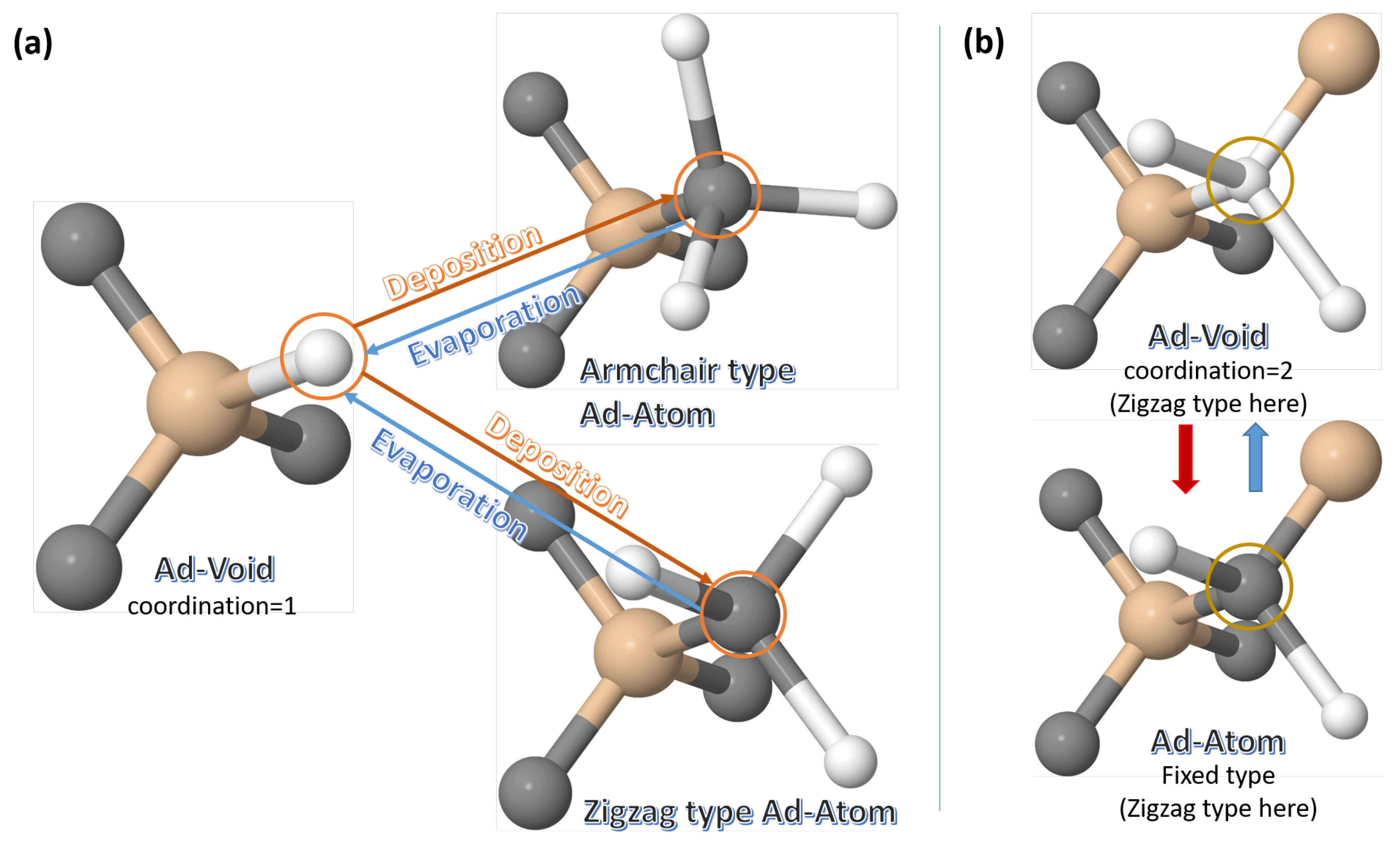
  • Kinetics is simulated by a stochastic sequence of evaporation/deposition events whose occurrence probability depends on the local configuration (see Figure 1);
  • Switching between cubic and hexagonal symmetry (Figure 1) can be statistically considered during the simulation and, as a consequence, the generation and evolution of extended defects can be predicted;
  • The default setting considers a compound material. In this case, atomic species (e.g., Si and C) undergo independent kinetics. An elemental material can be considered by means of symmetric calibrations for the two types of atoms;
  • The code allows for the study of point and extended defect generation at an atomic level, considering a non-ideal bonding configuration;
We have simulated the growth of Si and SiC nano-particles. Nano-crystal simulation is initialized from a small cubic seed although the results do not depend (within the intrinsic statistical variations of the approach) on the initial seed shapes. The parameters’ calibration used for cubic Si-C material is discussed in Ref. [10] while in the case of the Si nano-crystal a symmetric Si only calibration (i.e., the one of Ref. [10]) is used for the two types of atoms, in order to reproduce the behavior of a pure Si crystal. The probability of switching between cubic and hexagonal configuration for an ad-Atom with coordination 1 (see Figure 1) is set to zero (PtransZigZag=1.0) for the Si material while it is set to 0.5 (PtransZigZag = 0.5) for the Si-C case, in order to reproduce the meta-stability of different poly-types.

3. Results

The evolution of nano-particles and in general of non-planar substrates is one of the main application fields of our code. In Figure 2 we compare the shape of a simulated Si nano-particle with the one of a Si nano-crystal grown by ICP-CVD. We note that by using symmetric parameters for the evaporation we can effectively simulate the case of a mono-atomic crystal growth (a pure Si grain in this case). The simulated and real nano-particle shapes are in a noteworthy agreement. In both cases the nano-crystal shape is similar to an octahedron with dominant <111> facets while atoms at the edges tend to align along <311> planes. Apart from the surface structures, local vacancy type defects are visible (as red balls) by transparency in the bulk of the simulated nano-particle. Vacancy generation efficiency could be an important outcome of the simulation analysis, which can be also experimentally investigated in the application of these systems in the QT field. We could expect that the resulting vacancy density and space distribution depend on the process macroscopic conditions and this aspect can be considered in the code parameter calibration. Indeed, the density of vacancies trapped in the growing crystal in a simulated growth depends strongly on the deposition/evaporation parameter choice (for a discussion see Ref. [10]).
A comparison between the simulated and experimental SiC nanocrystal morphology is shown in In Figure 3. In the nano-particles obtained after the simulated growth the facets of the nano-grains tend to align along the <100> and <111> directions but the structure is rather irregular. The experimental analyses of SiC nano-crystal morphology and microstructures also show both a rather irregular nano-crystal shape and the occurrence of a strongly defective state dominated by stacking-fault-type extended defects. Our KMCsL code reproduces this behavior. In the central figure of the top panel of Figure 3 we show only the atoms which are not in epitaxial order with respect to the initial seed and we can observe the formation of stacking faults in the <111> facets of the growing nano-crystal. Consecutive switches causes the formation of different symmetries of SFs and a sequence of extended defects and regular crystal regions. In the high resolution analysis of the experimentally grown nano-particles (see left figure of the bottom panel of Figure 3) similar defective structures have been observed demonstrating the predictive potential of the code. Vacancy type defects are generated simultaneously to the extended ones (see left figure in the top panel of Figure 3) and both vacancy generation efficiency and the global morphology of the nano-crystal are affected by the SF defect formation.

4. Conclusions

In this manuscript we have applied a KsLMC approach to study the synthesis of nano-particles made by group IV elements with sp 3 -type bonding. The results here shown clearly demonstrate some code features which are appealing for its application as a support of the experimental activity related to the synthesis of materials with potential QT applications. The possibility to predict several “observables” of the growth kinetics (e.g., the speed of growth, the point defect density, the SF configuration and evolution, the shape evolution of microcrystalline objects, etc.) allows for an effective experimental verification of the code and for its use as support of experimental design of materials for QT applications. As for any parameter-reliant approach, a refinement of the calibration will be therefore necessary by fine tuning the parameters in order to link the simulation predictions to the experimental data for variable thermodynamic conditions of the growth processes.

Author Contributions

A.L.M. developed and implemented the code, M.C., I.D. and G.F. (Giuseppe Fisicaro) performed the simulations, G.M. performed the experiments; G.F. (Giuseppe Falci) discussed and reviewed the manuscript; A.L.M. wrote the paper.

Acknowledgments

This work has been partially supported by the CHALLENGE project (HORIZON 2020-NMBP-720827, http://www.h2020challenge.eu/), CHALLENGE is a research and innovation action funded by the European Union’s Horizon 2020 programme.

Conflicts of Interest

The authors declare no conflict of interest.

References

  1. La Via, F.; Camarda, M.; La Magna, A. Mechanisms of growth and defect properties of epitaxial SiC. Appl. Phys. Rev. 2014, 1, 031301. [Google Scholar] [CrossRef]
  2. Blase, X.; Bustarret, E.; Chapelier, C.; Klein, T.; Marcenat, C. Superconducting group-IV semiconductors. Nat. Mater. 2009, 8, 375. [Google Scholar] [CrossRef] [PubMed]
  3. Radulaski, M.; Widmann, M.; Niethammer, M.; Zhang, J.L.; Lee, S.Y.; Rendler, T.; Lagoudakis, K.G.; Son, N.T.; Janzen, E.; Ohshima, T.; et al. Scalable quantum photonics with single color centers in silicon carbide. Nano Lett. 2017, 17, 1782–1786. [Google Scholar] [CrossRef] [PubMed]
  4. Redman, D.; Brown, S.; Sands, R.; Rand, S. Spin dynamics and electronic states of N-V centers in diamond by EPR and four-wave-mixing spectroscopy. Phys. Rev. Lett. 1991, 1767, 3420–3423. [Google Scholar] [CrossRef] [PubMed]
  5. Camarda, M.; La Magna, A.; La Via, F. A kinetic Monte Carlo method on super-lattices for the study of the defect formation in the growth of close packed structures. J. Comput. Phys. 2007, 227, 1075–1093. [Google Scholar] [CrossRef]
  6. Bunea, M.M.; Dunham, S.T. Monte Carlo study of vacancy-mediated impurity diffusion in silicon. Phys. Rev. B 2000, 61, R2397. [Google Scholar] [CrossRef]
  7. Deretzis, I.; Magna, A.L. Interaction between hydrogen flux and carbon monolayer on SiC (0001): Graphene formation kinetics. Nanoscale 2013, 5, 671–680. [Google Scholar] [CrossRef] [PubMed]
  8. Deretzis, I.; Magna, A.L. Simulating structural transitions with kinetic Monte Carlo: The case of epitaxial graphene on SiC. Phys. Rev. E 2016, 93, 033304. [Google Scholar] [CrossRef] [PubMed]
  9. Camarda, M.; La Magna, A.; Fiorenza, P.; Giannazzo, F.; La Via, F. Defect formation and evolution in the step-flow growth of silicon carbide: A Monte Carlo study. J. Cryst. Growth 2008, 310, 971–975. [Google Scholar] [CrossRef]
  10. La Magna, A.; Alberti, A.; Barbagiovanni, E.; Bongiorno, C.; Cascio, M.; Deretzis, I.; La Via, F.; Smecca, E. Simulation of the Growth Kinetics in Group IV Compound Semiconductors. Phys. Status Solidi A 2018, 1800597. [Google Scholar] [CrossRef]
Figure 1. Schematic of the local bonding rearrangement due to deposition/evaporation events in the case of coordination = 1 value (Coor = 1) [panel (a)] and Coor = 2 [panel (b)]. Large gray and light brown spheres indicate Ad-Atoms (e.g., C and Si) while small white spheres indicate Ad-Voids. For a deposition event in the case of coordination = 1 value (Coor = 1) the local bonding configuration (Armchair or Zigzag) has to be statistically selected. The bonding network is undetermined for an AdVoid with Coor = 1 while it is fixed for both an Ad-Void and Ad-Atom with Coor = 2 and Coor = 3, see e.g., panel (b) where a Zigzag type of bonding is shown.
Proceedings 12 00032 g001
Figure 2. (a) Transmission electron microscopy of a silicon nanocrystal grown by the plasma assisted process. The diffraction analysis in the inset evidences the diamond configuration. (b) Snapshot of the simulated growth process of a silicon nano-crystal starting from a cubic seed. Only under coordinated surface atoms and vacancies (red spots) are shown.
Proceedings 12 00032 g002
Figure 3. Top panel: snapshot of the simulated growth process of a silicon carbide nanocrystal starting from a cubic seed. In the left figure only under coordinated surface atoms and vacancies (red spots) are shown. In the center figure, the atoms which are not in epitaxial order with the seed. In the right figure, the vacancy distribution in the bulk region of the nanocrystal. Bottom panel in the left figure examples of configurations (analyzed by transmission electron microscopy) of a silicon carbide nanocrystal grown by a plasma assisted process are shown. In the right figure, high resolution analysis of one nanocrystal reveals stacking fault-type defects.
Proceedings 12 00032 g003
Publisher’s Note: MDPI stays neutral with regard to jurisdictional claims in published maps and institutional affiliations.

