Abstract
Laser-microstructured double-sided biocompatible adhesive tapes as intermediated bonding layers are potential candidates for hybrid integration of a disposable biochip. In the EU-PHOCNOSIS project, such thin adhesive tapes are proposed to integrate the polymer microfluidic system with the optical sensor chip. Three laser-assisted structuring methods are investigated to efficiently transfer microchannel patterns to the adhesive tape at room temperature. The test structure design consists of a single channel with 400 µm wide, 30 mm length and two circular receivers with 2 mm radius. The best structuring results are found by using a UV picosecond laser.
1. Introduction
Highly-sensitive Point-of-Care (PoC) tests are significantly important for early diagnosis of cardiovascular diseases and infectious diseases. Optical biosensors [1] based on photonic integrated circuit (PIC) platform is the most promising technology for covering the current demand of PoC devices. They combine high-sensibility and label-free detection techniques with cost effectiveness. PICs consist of functional photonic components integrated into a millimeter-sized device. Their fabrication process is made with a wafer-scale technology allowing mass production. However, for biosensing applications, they need a low-cost, reliable and robust integration with a microfluidic system. The double-sided tapes are excellent candidates for bonding due to their unique properties such as cheap, reliable, biocompatible and easy-to-pattern by laser cutting techniques. They have been recently demonstrated for microfluidics applications [2], where a simple and rapid prototyping of 1.5 mm-width channels can be carried out via a CO2 laser system. Tapes are found in various thicknesses and can be easily integrated at room temperature with different materials e.g., polymer, silicon and glass.
As a part of the EU-PHOCNOSIS project, laser-microstructured double-sided adhesive tapes have been proposed for hybrid integration of a disposable biochip. Such thin adhesive tapes are used as intermediated bonding layers between the polymer microfluidic system and the PIC-based sensor chip. Here the tape should be patterned in a micrometer scale in order to have access between the polymer microchannels and the photonic sensing microstructures. Three laser-assisted structuring methods are investigated to efficiently transfer channel patterns to the adhesive tape at room temperature. Laser-structured microchannels in tapes are bonded with a blank polymer substrate and a blank silicon (or glass) substrate. As a proof of concept, the hybrid integration is tested using ID-water. Structuring tests related to the reduction of channel widths are also considered in this work. Finally, this simple and fast laser structuring technique can be suitable for large-scale manufacturing of narrow channels (≤100 µm in width) in a reliable and effective way.
2. Materials and Methods
2.1. Double-Sided Adhesive Tapes
The target tape (ARclear® 8932EE) from Adhesives Research Inc. (Glen Rock, PA, USA) exhibit some benefits related to long-term durability, environmental resistance (extreme temperature, humanity and UV light) and easy processing & bonding. The tape architecture consists of three layers of materials that include the 40 µm thick biocompatible adhesive layer placed in the middle of two polyester release liners with thicknesses of 50 µm.
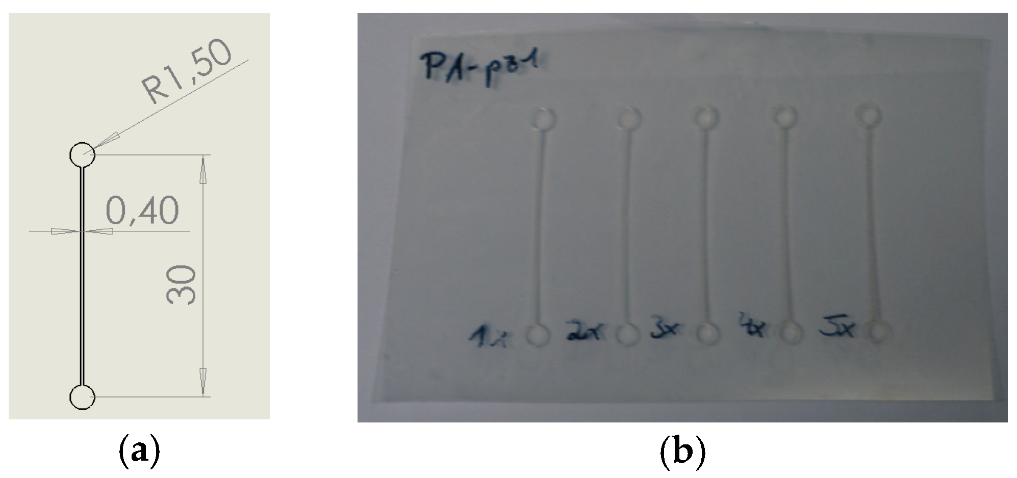
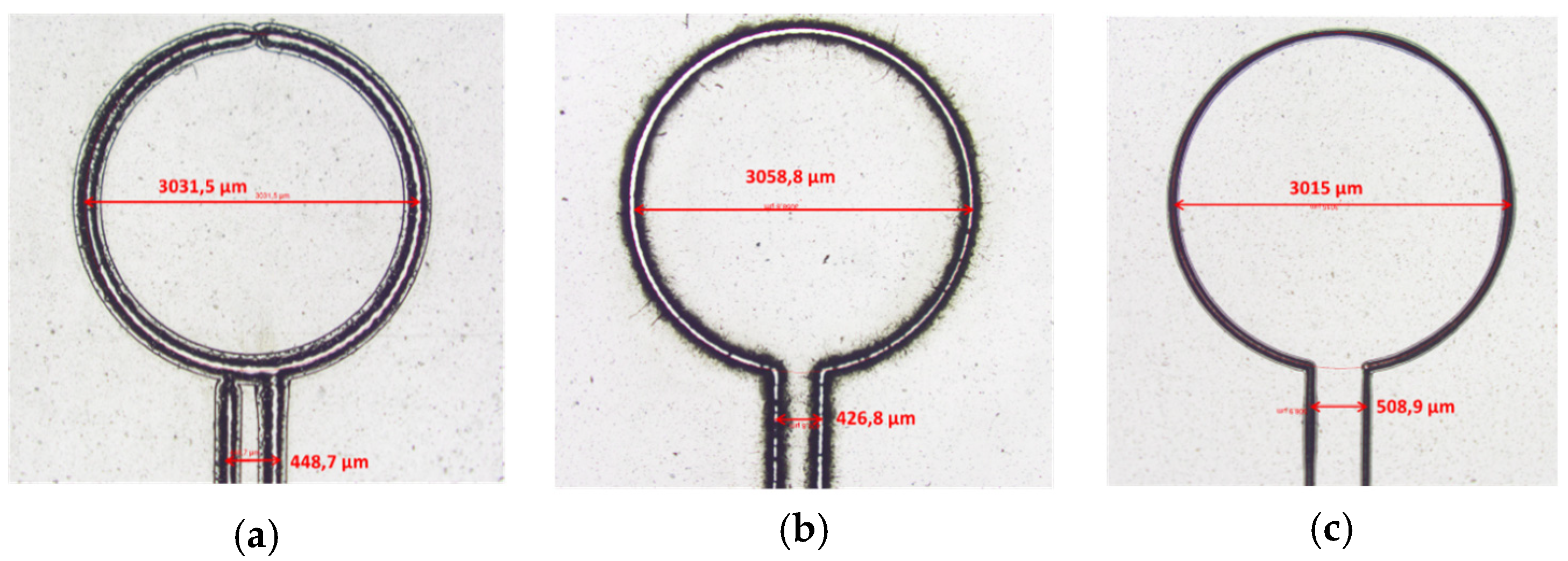
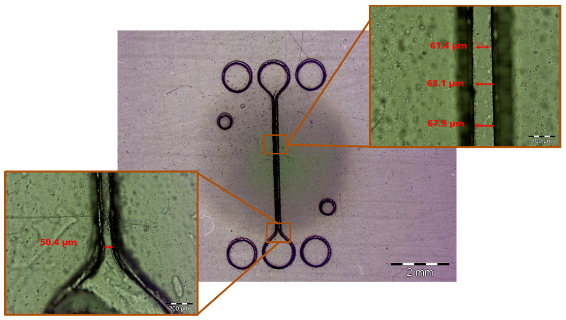
2.2. Laser Structuring Methods
Three laser-assisted structuring systems are used: (1) 30 W CO2 laser with spot beam of 200 µm and centered at λ = 10.6 µm, (2) green pulsed laser [3] with spot beam of 50 µm and centered at λ = 532 nm and (3) Nd:YVO4 Picosecond UV laser (ps UV laser) [4] with spot beam around 10–30 µm and centered at λ = 355 nm. The procedure of the three automated methods is similar. The CAD design is simply loaded in the system and later transferred to the tape. The process parameters were optimized in order to obtain non-carbonized and straight walls.
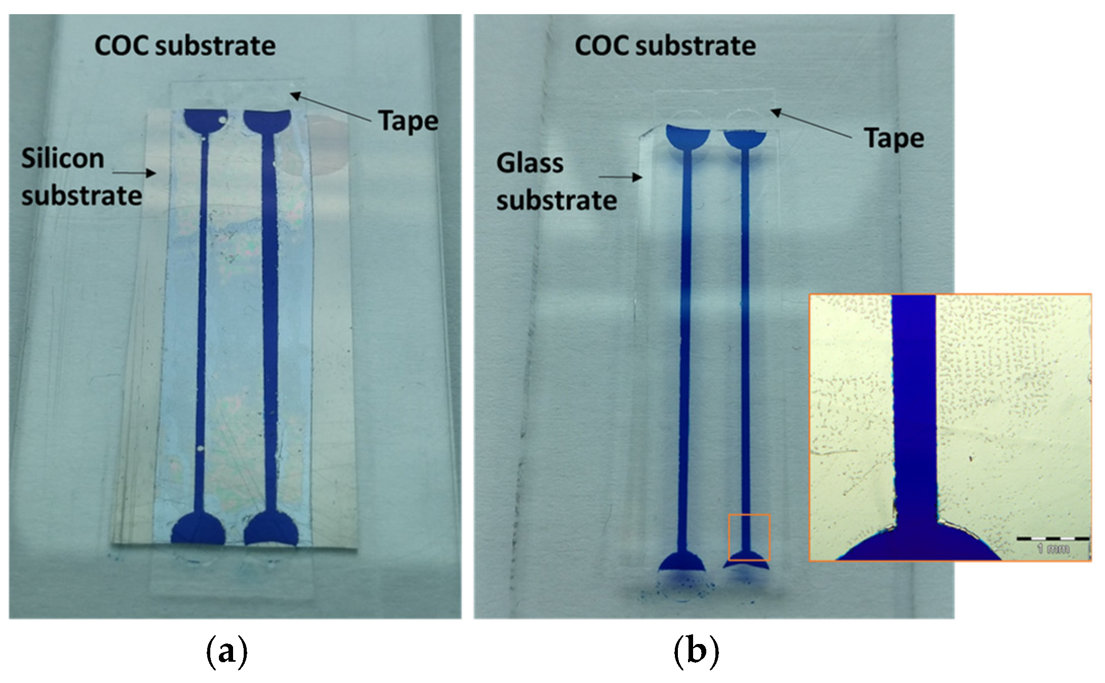
2.3. Preliminary Bonding and Leakeage Tests
In order to test the bonding between two different materials via tapes, blank material substrates were used. First, the structured tape was sealed manually to a silicon (or glass) substrate. Later, the second substrate made with cyclic olefin copolymer (COC) material was also sealed to the tape. The leakage tests of the hybrid substrate were realized by flowing colored DI-water through the patterned channel of the tape. Here a syringe was used to pump manually the liquid through the channel.
3. Results and Discussion
Laser structuring tests are realized using a single-channel design, which is transferred to the 8932EE tape. The single channel has a width of 400 µm while the ports exhibit a circular shape with diameters of 3 mm, see Figure 1a. As an example, Figure 1b illustrates five patterned channels over an area of ~7 × 3.6 cm2, which are made with the CO2 laser system. Here the resulting widths (510–600 µm) of the tape channel are larger than the width (400 µm) of the layout design. This difference is caused by the laser beam diameter of 200 µm.
Figure 1.
(a) Layout design of the single microchannel; (b) First tape sample structured by using a CO2 laser with optimized power of ~2 W. This sample includes an array of five channels.
In order to reduce the dimensions of patterns written on tapes, the use of two lasers with smaller spot beam size has been investigated. Figure 2 illustrates microscope images of three channels written on the tape by using CO2 laser, pulsed green laser and ps UV laser. A huge advantage is observed by structuring the tape with the ps UV laser. The microscope inspection of the cross section of the ps UV laser structured tape is also realized, resulting channels with smooth and straight walls.
Figure 2.
Microscope images of the structured receiver on the tape using (a) 200 µm spot CO2 laser; (b) 50 µm spot pulsed green laser and (c) 10–30 µm spot ps UV laser.
A simple bonding test of ps UV laser patterned tapes was realized by using colored DI-water, which is introduced in the receiver via a syringe. Two hybrid substrates were tested as shown in Figure 3. The left image shows a bonded sample composed by a silicon substrate and COC substrate, while the second image illustrates a hybrid sample that consists of a glass substrate and a COC substrate. In both samples, the blue DI-water flows through the single channel and is not penetrated into the channel walls, see inset image. Hence, successful leakage tests of tape-bonded substrates are demonstrated where a good alignment between the tape and both substrates should be performed.
Figure 3.
Leakage tests realized in bonding samples by using colored DI water. The ps UV laser structured tape joins the COC polymer substrate to (a) the blank silicon substrate and (b) the blank glass substrate. Note that, the tape joins both substrates perfectly where the water flows smoothly through the channel without leakages (see inset image).
This structuring method is being developed in order to manufacture channels with widths ≤100 µm. Figure 4 gives the microscope images of the first narrow channel transferred to the tape. They show good results. However, the resulting width of the tape channel (122 µm) is two times larger than the width of the tape strip (50–68 µm). According to these results, an optimization of the structuring process is still needed in order to reduce the fabrication tolerances.
Figure 4.
Microscope images of the first narrow channel fabricated via UV ps laser. The widths of the strip tape are ranging from 50 µm to 68 µm. This tape strip is removed before bonding.
4. Conclusions
We demonstrate the fabrication of microchannels in double-sided adhesive tapes by using three different laser structuring approaches. The best structuring results are found by using a ps UV laser where patterned channels with a nominal width of 400 µm exhibit smooth and straight walls. The hybrid integration of silicon (or glass) and COC substrates was realized by using such laser-microstructured tapes and successfully tested with colored DI-water. Additionally, preliminary narrow channels (122 µm in width) are transferred to the tape in order to match the structural dimensions of both functional chips. The bonding technology based on narrow-channel tapes is a promising approach for optimal integration of a disposable biochip where alignment & dicing tolerances, and cleaned tape surfaces are aspects need to be taken into account. The advantage of automated laser structuring systems is that they allow mass production. In an area of 10 cm × 10 cm, a total number of 88 patterns can be quickly transferred to the tape.
Acknowledgments
This work is supported by Horizon 2020 within the objective HEALT-PHC10-2014, project “PHOCNOSIS” with a grant agreement number of 634013. Also thanks to S. Karaszkiewicz from Fraunhofer IZM for ps UV laser structuring and A. Murr from CDA for providing the 400 µm channel design.
Conflicts of Interest
The authors declare no conflict of interest.
References
- Estevez, M.C.; Alvarez, M.; Lechuga, L.M. Integrated optical devices for lab-on-a-chip biosensing applications. Laser Photon. Rev. 2012, 6, 463–487. [Google Scholar] [CrossRef]
- Patko, D.; Mártonfalvi, Z.; Kovacs, B.; Vonderviszt, F.; Kellermayer, M.; Horvath, R. Microfluidics channels laser-cut in thin double-sided tapes: Cost-effective biocompatible fluidics in minutes from design to final integration with optical biochips. Sens. Act. 2014, 196, 352–356. [Google Scholar] [CrossRef]
- Böttger, G.; Queisser, M.; Arndt-Staufenbiel, N.; Schröder, H.; Lang, K.D. Building blocks for actively-aligned micro-optical systems in rapid prototyping and small series production. In Proceedings of the SPIE Photonics West Conference, San Francisco, CA, USA, 9–11 February 2015. [Google Scholar]
- Raciukaitis, G.; Gedvilas, M. Processing of polymers by UV picosecond lasers. In Proceedings of the 24th International Congress on Applications of Lasers & Electro-Optics (ICALEO), Miami, FL, USA, 31 October–3 November 2015. [Google Scholar]
Publisher’s Note: MDPI stays neutral with regard to jurisdictional claims in published maps and institutional affiliations. |
© 2017 by the authors. Licensee MDPI, Basel, Switzerland. This article is an open access article distributed under the terms and conditions of the Creative Commons Attribution (CC BY) license (https://creativecommons.org/licenses/by/4.0/).