1. Introduction
The very important key characteristic of the Hall sensors is the offset voltage V
off, which is its output signal in the absence of magnetic field [
1,
2,
3]. It depends on power supply, temperature, mechanical stress and sometimes it is larger than the Hall voltage V
H (
B). Some efforts to reduce the initial offset V
off by hardware consists of orthogonally coupling of two or more matched symmetrical Hall plates [
2]. But, after applying this method, the residual offset is large since the matched Hall plates are not identical. An alternative effort to reduce the initial offset V
off, is the spinning current method [
3,
4,
5], or “dynamic offset cancellation” [
1]. In the spinning-current method, the direction of current flow in a single symmetrical Hall plate is made to spin around an axis through the center of the Hall plate. At the same time, the output voltage is sampled at the Hall contact pair which is perpendicularly oriented to the current flow [
2]. The very common Hall sensors are four terminal devices [
1,
6,
7,
8,
9,
10], where one pair of opposite terminals serves as drive contacts and the other pair as sense contacts; consequently Hall sensors can be operated in two [
1] or four [
3] different modes. During an offset cancelling measurement cycle, the drive current is spatially rotated through these modes and the corresponding output signals are averaged [
1,
6,
7,
8,
9,
10].
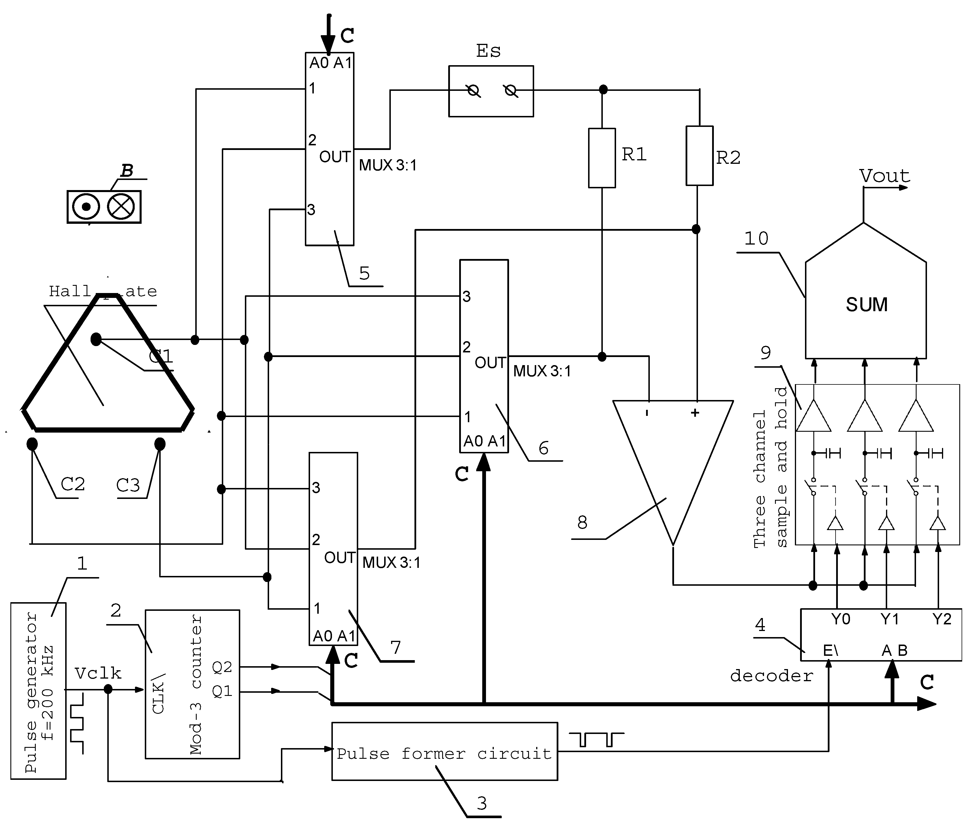
This paper presents a novel Hall magnetometer using dynamic offset cancellation principle, based on a single equilateral triangular n-Si plate with three contacts only. The functions, necessary for obtaining the useful Hall signal and cancelling the offset, are performed by proper interface electronics. Moreover, this device is characterized by high spatial resolution due to the small number of Hall plate contacts (three only).
2. The Hall Plate Design and Magnetometer Operation Principle
The Hall plate consists of a semiconductor
n-Si structure in the form of an equilateral triangle,
Figure 1. The magnetosensitivity is about 25 V/AT. On the surface of the substrate, near the vertices of the triangle, three
n+-contacts, C
1, C
2, and C
3 are positioned.
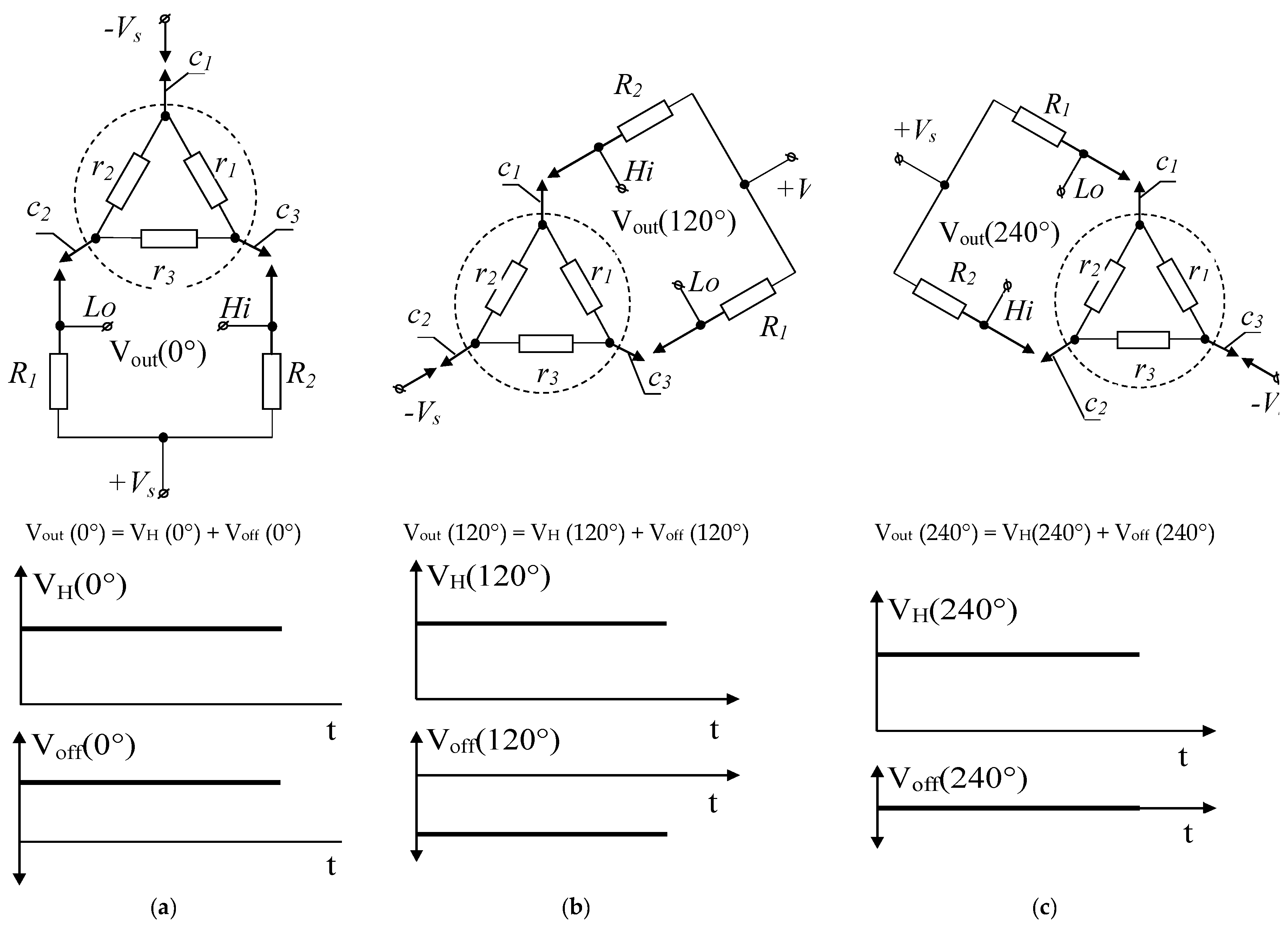
The dynamic offset-cancelling measurement cycle includes three consecutive states, shown in
Figure 2a–c. We shall call them 0° state, 120° state and 240° state respectively. In
Figure 2a–c, for the convenience of analysis, the Hall element is represented by a model of three connected in triangle resistors—r
1, r
2 and r
3. As is shown, during each state, an external circuit is connected to the plate contacts in a certain way. Such external circuit comprise the power supply with terminals −V
S and +V
S and the resistor network R
1–R
2 (R
1 = R
2 = R). One terminal of R
1 as well as one terminal of R
2 is connected to the power supply terminal +V
S. The other terminal of R
1 as well as the other terminal of R
2 is switched to a certain pair of adjacent plate contacts. To the third plate contact, the power supply terminal −V
S is switched. Between the terminals Lo and Hi, the sensor output voltage V
out is measured. In general, V
out consists of two parts, namely the magnetic field dependent Hall voltage V
H (
B) and the offset voltage
Voff:
The Hall plate is fed with constant current as the value of external resistors R1 and R2 many times exceed the value of r1, r2 and r3.
The first state of the measurement cycle (0° state) is shown in
Figure 2a. The resistor R
1 is switched to contact
C2, the resistor R2 is switched to contact c3, and the power supply terminal −VS is switched to contact c1. For an ideal Hall plate, the resistances of r1, r2, and r3 are equal, i.e., r1 = r2 = r3 = r. The resistors r1, r2, R1 and R2 form Wheatstone bridge. In the absence of magnetic field, the output voltage measured between the terminals Lo and Hi will be zero, because the bridge is balanced. In the presence of magnetic field, the Lorentz force FL = qVdr × B deflects the moving carriers laterally; q is the electron charge and Vdr is the velocity of the carriers. As a result, in the vicinity of the contacts C2 and C3 additional charges are generated, resulting in appearing of Hall voltage between the contacts Hi and Lo. The Hall voltage is proportional to the magnitude of the magnetic field B, and its sign depend on the direction of the magnetic field B.
Assume that an imbalance, for example due to a mechanical stress, occurs such that the region between the contacts c
1 and c
2 shows a resistance smaller than the rest of the plate, i.e.,
r1 =
r3 =
r;
r2 = r—Δ
r. In such case, in absence of magnetic field
B, (
B = 0), the output voltage
Vout between the contacts Lo и Hi will be different from zero as the bridge (
r1–
r2–R
1–R
2) is not balanced due to
r1 ≠
r2. To the terminal Lo, the resistor
r2 is connected, corresponding to the substrate region with resistance
r–Δ
r, and to the terminal Hi, the resistor
r1 is connected, corresponding to the substrate region with resistance
r. Then, the offset voltage V
off (0°) will be measured,
Figure 2a. In the presence of magnetic field
В (
B ≠ 0), the Hall voltage
VH between the contacts Lo и Hi appeared, which is added to the offset voltage V
off (0°). In particular direction of the magnetic field, the Hall voltage V
H (0°) will have the same sign as the offset voltage V
off (0°), as is shown in
Figure 2a.
The second state of the measurement cycle (120° state) is shown in
Figure 2b. Actually, switching contacts during the transition from the first to second state is carried out in such a way that the external circuit rotated virtually in the Hall element plane around its center to an angle 120° from its initial position,
Figure 2b. In such case, the bridge
r2—r3—R
1—R
2 is not balanced due to
r2 ≠
r3. To the terminal Lo, the resistor
r3 is connected, corresponding to the substrate region with resistance
r, and to the terminal Hi, the resistor
r2 is connected, corresponding to the substrate region with resistance
r–Δ
r. This means that the measured between contacts Lo and Hi offset voltage V
0 (120°) will have the same value but opposite sign compared to the measured offset voltage V
0 (0°) during the first state of the measurement cycle (0° state) shown in
Figure 2a. As can be seen from the scheme, the measured Hall voltage V
H (120°) between the output contacts Hi and Lo will have the same sign compared to the measured Hall voltage V
H (0°) during the first state (0° state).
The third state of the measurement cycle (240° state) is shown in
Figure 2c. Actually, switching contacts during the transition from the first to third state is carried out in such a way that the external circuit rotated virtually in the Hall element plane around its center to an angle 240° from its initial position,
Figure 2c. In such case, the bridge (
r1–
r3–R
1–R
2) is balanced due to
r1 =
r3. This means that the measured between the contacts Lo and Hi offset voltage V
0 (120°) will be zero, i.e., V
0 (120°) = 0. As can be seen from the scheme, the measured Hall voltage V
H (120°) between the output contacts Hi and Lo will have the same sign compared to the measured Hall voltages V
H (0°) and V
H (120°) during the first state (0° state) and second state (120° state).
In the end, the obtained voltages from each of the three consecutive states from the current measurement cycle are summed. This way, the useful Hall signal triples but the offset voltages are cancelled in most cases:
where V
res is so-called residual plate offset, which is very low.


