Article

Power-Efficient Electronically Tunable Fractional-Order Filter

1
Department of Electronics Engineering, Indian Institutes of Technology Dhanbad, Dhanbad 826004, India
2
Department of Telecommunications, Brno University of Technology, Technicka 12, 61600 Brno, Czech Republic
*
Author to whom correspondence should be addressed.
Fractal Fract. 2024, 8(1), 31; https://doi.org/10.3390/fractalfract8010031
Submission received: 6 November 2023 / Revised: 11 December 2023 / Accepted: 19 December 2023 / Published: 30 December 2023
(This article belongs to the Section Engineering)

Abstract

:
This article describes a low-voltage, low-power fractional-order low-pass filter (FO-LPF) of order 1 + α, which is implemented using a voltage differencing differential difference amplifier (VDDDA). The VDDDA structure is implemented using the bulk-driven metal oxide semiconductor transistor technique. The transistors operate in the subthreshold region to maintain low-supply voltage and low-power consumption. The FO-LPF structure implemented using this VDDDA structure is compact. It includes three VDDDAs and three grounded capacitors along with two active resistors implemented using MOS transistors. In addition, this filter structure provides electronic tuning of its order and cut-off frequency through the bias current of the active component used. The effects of tracking error and parasitics on the functionality of the proposed FO-LPF were investigated. The VDDDA and filter operate at ±300 mV and dissipate only 207 nW and 663 nW of power, respectively. Thus, the VDDDA structure and filter are suitable for low-voltage and low-power operation. Layouts of the proposed VDDDA as well as the FO-LPF were designed in the Cadence Virtuoso environment. Post-layout simulation results of the designed circuits imply that they are suitable for fabrication. Noise, total harmonic distortion, Monte-Carlo, and PVT analyses were also performed.

1. Introduction

The utilization of fractional calculus (FC) is being observed increasingly within the engineering domain due to its ability to provide a more precise representation of natural phenomena and physical entities compared to integer-order (IO) models, making their study and control easier. Fractional-order (FO) systems offer greater design flexibility compared to IO systems. FO systems provide more design adaptability than IO systems. Although the mathematical basics of FC evolved around 200 years ago, this topic remained restricted only to mathematicians until it found its importance in diverse engineering fields, such as material theory, diffusion theory, control theory, bioengineering, circuit theory and design, electromagnetics, and robotics. In the case of circuit theory, fractional-order systems find applications in transmission media, power electronics, multivibrator circuits, integrator–differentiator circuits, chaotic systems, oscillators, resonators, filters, memristive elements, and many more [1,2,3,4]. The demand for active filters in diverse fields, including analog signal processing, is experiencing a significant surge. The order of a filter is a significant attribute, which is determined by its slope in the transition band. Order is generally a real number, but while designing a filter using traditional methods, it is rounded off to the nearest integer. Therefore, accurate requirements for frequency response are not achieved. Nevertheless, the FO design methodology enables researchers to have precise control over the various parameters of the filter. IO filters have a slope of −20 × n dB/decade, where n is a positive integer. Fractional order filters (FOFs), a generalized case of IO filters, have a slope of −20 × (n + α) dB/decade for an FOF of order (n + α), where n is a positive integer and α is a real number between 0 and 1 [4,5].
The successful implementation of FOFs necessitates the use of fractional-order passive elements (FOEs). These FOEs can be fractional-order capacitors (FOCs) or fractional-order inductors (FOIs). The commercial viability of FOEs has yet to be achieved, despite numerous attempts to manufacture them [3,4]. Because of the above-stated reason, for designing FOFs, integer-order approximations are used. There are two design techniques [3,6]. One approach involves approximation of integer-order capacitors and integer-order inductors by FOCs and FOIs, and thus, a generalized form of conventional filters in the fractional domain is obtained. The approximation mentioned above can be achieved by approximating FOEs by building RL or RC networks [3,4,7]. Using this approach, several structures are present in the literature where operational amplifier (OPAMP) [8,9], second-generation current conveyor (CCII) [10], operational transconductance amplifier (OTA) [11], and differential voltage current conveyor (DVCC) [12,13] are used as active elements. Nevertheless, the utilization of this approximation to create FOFs is accompanied by the disadvantage of incorporating floating resistors and capacitors during the implementation of FOEs [4,7]. Additionally, the obtained filter does not provide tuning of its order. The second approach is to approximate properly the transfer function (TF) of FOFs through a suitable integer-order approximation. To implement this technique, the Laplacian variable (τs)α, is approximated using continued fraction expansion (CFE), a commonly used approximation technique. Several filter structures that use this approach are available in the literature. These implementations are achieved by utilizing OPAMP [14], current feedback operational amplifier (CFOA) [15,16], OTA, current follower (CF), and adjustable current amplifier (ACA) [17,18], differential difference current conveyor (DDCC) [19], current differencing buffered amplifier (CDBA) [20], and universal voltage conveyor (UVC) [21] as their active building blocks.
The voltage differencing differential difference amplifier (VDDDA) block, first described in [22], is a truly versatile analog building block that has a combined feature of OTA and differential difference amplifier (DDA). Therefore, the VDDDA block proves to be advantageous in situations where the tuning of filter parameters and summing of voltages are required simultaneously, as it makes the design compact. A literature survey of VDDDA-based filters reveals several available structures, such as multifunction filters [23], universal filters [24,25], or all-pass filters [22]. Out of all these filters, only [25] presents VDDDA based on the LV-LP technique, and it is also observed that until now, VDDDA has not been employed for the implementation of FOF.
Among the existing works, only [19] provides a filter structure that is capable of operating at low-voltage supply (LV) and low-power consumption (LP), because the DDCC structure is implemented using the bulk-driven quasi-floating gate (BD-QFG) technique. Generally, fractional-order filters are meant to be utilized in the processing of biological signals. Therefore, the utilization of the LV-LP technique would yield significant advantages in the implementation of such filters. The bulk-driven (BD) technique is considered a viable strategy for operating analog circuit designs in LV-LP conditions. This technique eliminates the barrier posed by the threshold voltage in the signal path. However, BD MOSFET offers bulk transconductance, which is three to five times lower than that of gate-driven MOSFET. This low transconductance value of the BD MOSFET leads to a lower intrinsic voltage gain and a reduced bandwidth for the resulting circuit. However, these limitations can be leveraged as a desirable characteristic for applications such as biomedical, as biological signals typically exhibit a frequency range of 0.05 to 10 kHz and amplitude levels ranging from 0.015 to 5 mV, and also because their prime requirements are low-voltage operation and lower power consumption. Operating BD MOSFET in the subthreshold region seems to be a great option to attain low power and low-frequency operation in electronic gadgets.
A fractional-order low-pass filter (FO-LPF) is often used in the detection of sleep apnea syndrome [26]. Due to sleep apnea, there is a prolongation of cardiac inter-beat intervals. These prolongations are detected by applying the energy signal obtained from an electrocardiogram (ECG) to an FO-LPF. In the realm of wearable biomedical systems, the utilization of low-power systems becomes imperative due to the critical significance of minimizing dissipation power. For instance, in an electrocardiogram (ECG) acquisition system, a low-pass filter (LPF) is employed to eliminate noise [27,28].
The aforementioned studies show that only a few structures of FOF are available for its operation in the LV-LP domain and that the mentioned benefits of VDDDA have not been explored in designing FOF. Therefore, this study presents the implementation of the proposed VDDDA using bulk-driven MOSFETs and operated in the subthreshold region. The CMOS structure has a power supply range of ±300 mV and power dissipation of 207 nW, rendering it well-suited for applications that require low voltage and low-power consumption. Subsequently, the FOF structure is implemented using the proposed VDDDA. The CFE method is employed as an approximation technique for the fractional operator, and the resulting circuit is realized using IFLF topology. The proposed FOF structure utilizes a minimal configuration consisting of three VDDDAs, six MOS transistors, and three grounded capacitors. The filter circuit operates with a power supply of only ±300 mV and has a power consumption of 663 nW. These values are the least among the compared literature studies. Additionally, the filter also offers electronic and independent tuning of its order and pole frequency. The remainder of the article is organized as follows. Section 2 analyzes VDDDA behavior, its proposed structure using the LV-LP technique, and simulation results. Section 3 presents the proposed VDDDA-based fractional order low-pass filter, its non-ideality analysis, and simulation results. A comparison of the proposed filter with the FOFs available in the literature is given in Section 4, followed by conclusions in Section 5.

2. Voltage Differencing Differential Difference Amplifier: VDDDA

2.1. Proposed VDDDA

A VDDDA is the active building block (ABB) that provides the advantages of both OTA as well as the differential difference amplifier (DDA). Figure 1a,b, shows the circuit symbol and behavioral model of VDDDA, respectively. VDDDA is a six-terminal block. Out of six terminals, there are four high-impedance voltage input terminals, V+, V, n, and p, a high-impedance auxiliary current output terminal z, and a low-impedance voltage output terminal w. The terminal relationships for an ideal VDDDA are characterized as follows [22]:
I z = g m ( V V + V V ) ,   V w = V z V n + V p ,
In (1), gm represents transconductance, and its relationship with bias current (Ib) is given as g m = I b / ( η V t ) . Here, Vt = KT/q is the thermal voltage and η is the subthreshold slope parameter which is a technology-dependent constant.
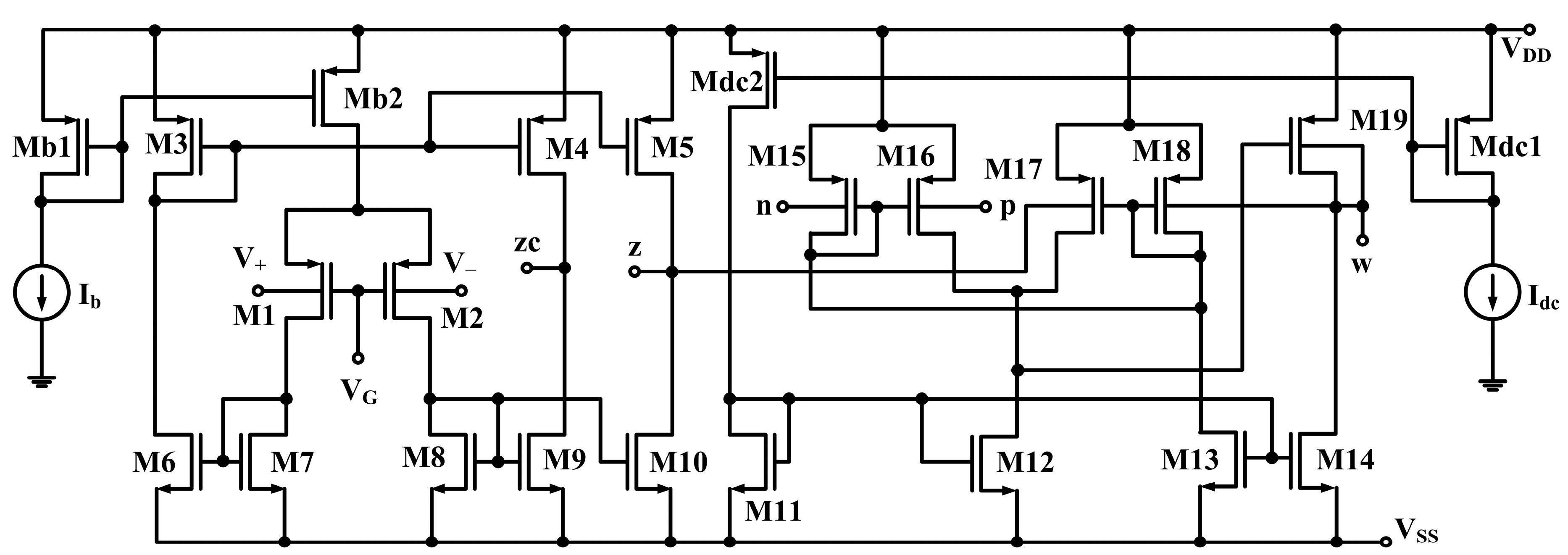
The CMOS structure for the proposed BD-VDDDA capable of operating at low voltage is shown in Figure 2. The first stage is the OTA stage, composed of MOSFETs M1–M10, where MOSFETs M1 and M2 are the bulk-driven PMOS input transistors, and MOSFETs M7 and M8 act as an active load. MOSFETs M5, M10, and M4, M9 act as a current mirror to obtain the output current and its copy at the zc terminal, respectively. For MOSFETs M1 and M2, input is applied at the bulk terminal, and the gate terminal is biased using a constant voltage source, VG. The second stage is the differential-difference stage comprising MOSFETs M11–M19. The two differential stages at the output are implemented using bulk-driven PMOS transistors M15–M16 and M17–M18. The output terminal, i.e., the drain of MOSFET M19, is shorted to the bulk terminals of MOSFETs M19 and M18 to create a negative feedback loop to improve the accuracy of the gain of the resulting voltage follower. The optimal aspect ratio of the MOSFETs used for the CMOS implementation of VDDDA is mentioned in Table 1. A detailed analysis of structure presented in Figure 2 is available in Appendix A.

2.2. Simulation Results of VDDDA

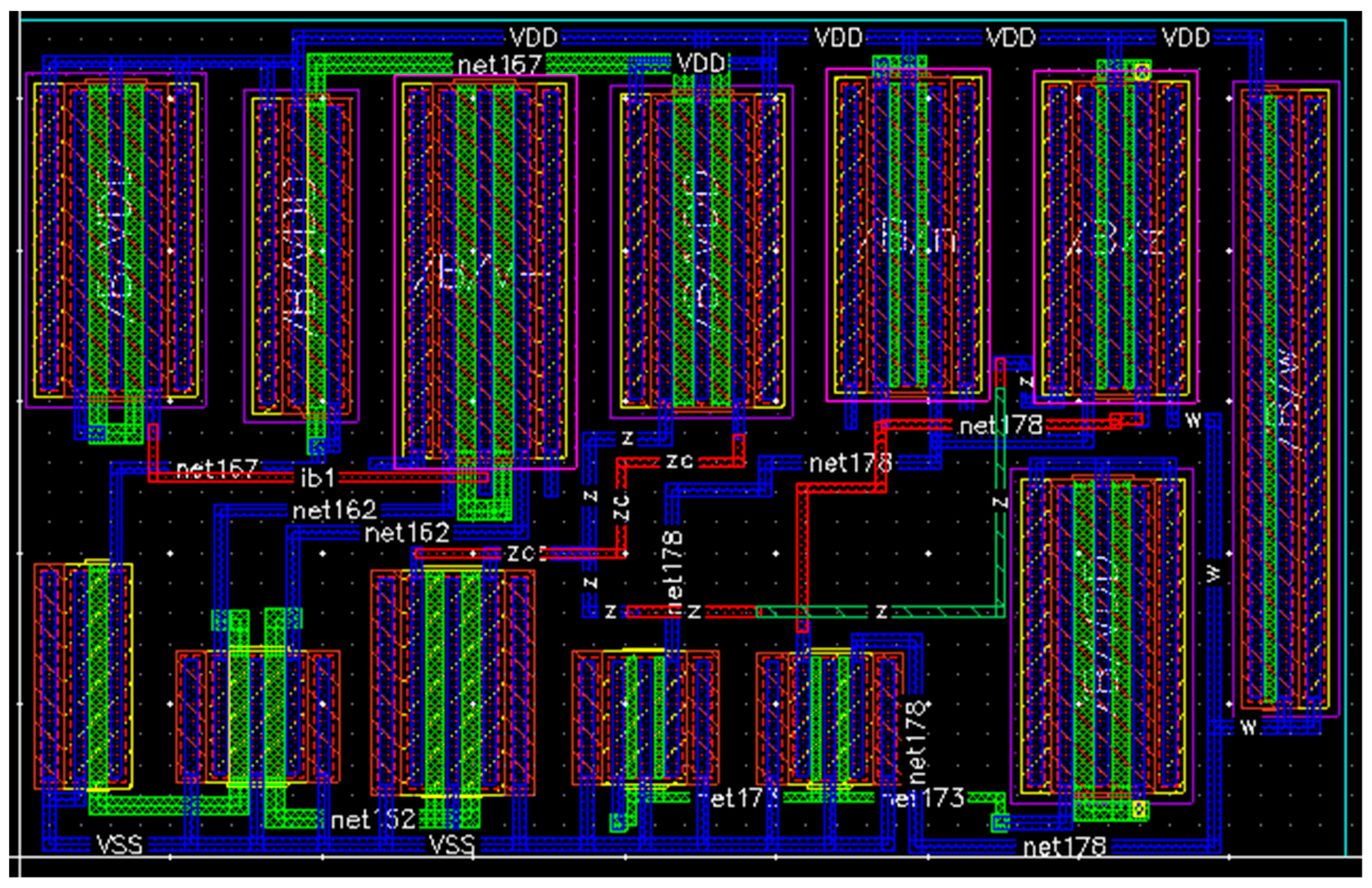
The bulk-driven CMOS circuit of LV-LP VDDDA operating in the subthreshold region, as shown in Figure 2, is simulated in the Cadence Virtuoso design tool using a 0.18 μm TSMC process parameter with supply voltages, VDD = −VSS = 300 mV and VG = −300 mV. The bias currents Ib and Idc are set to 14 nA and 55 nA, respectively. All the MOS transistors are operated in the subthreshold region, to derive the complete circuit at the lowest possible supply voltage for obtaining low power consumption. The proposed layout of the BD VDDDA circuit covers an overall area of 1208 μm2 (43.8 μm × 27.6 μm) and is shown in Figure 3.
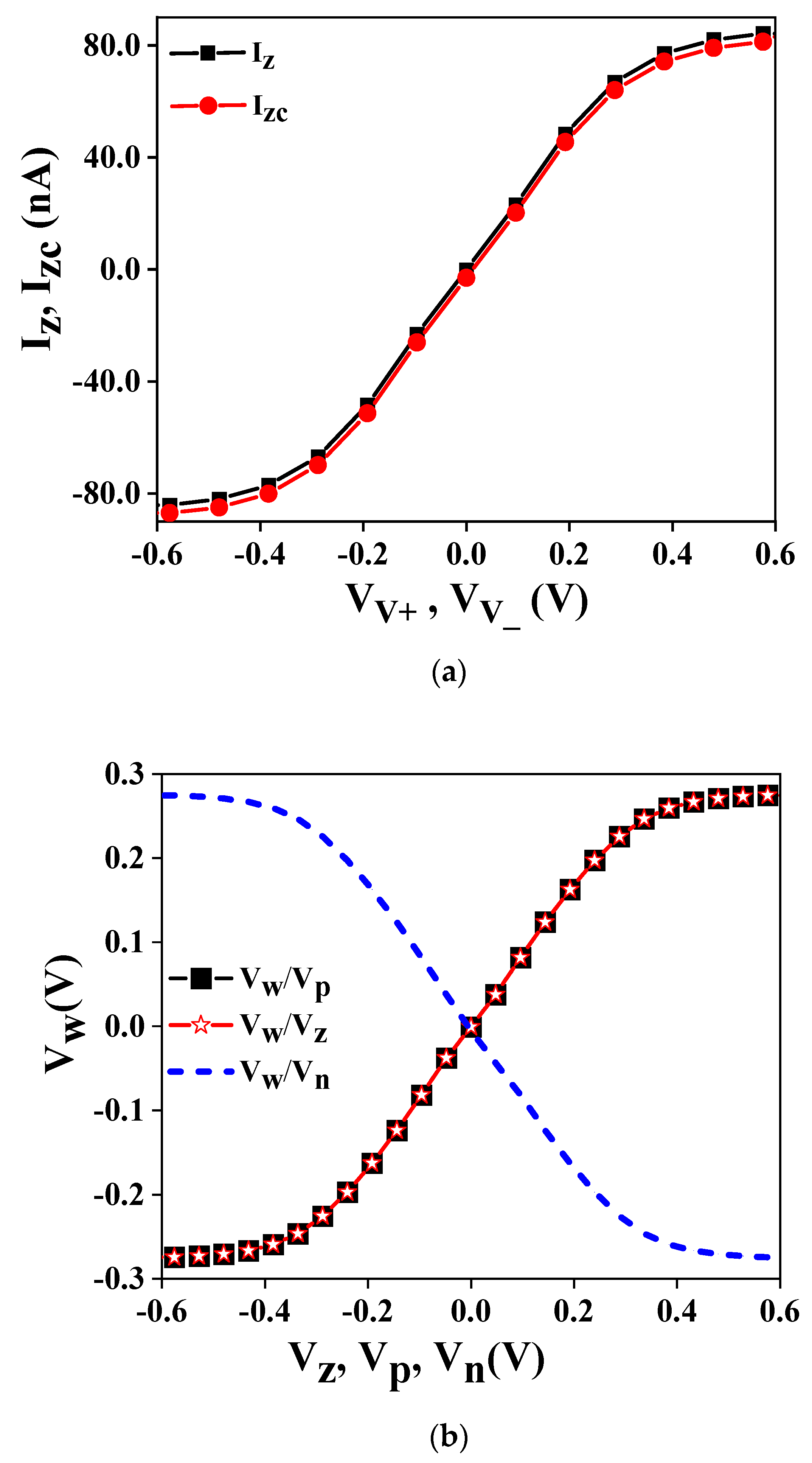
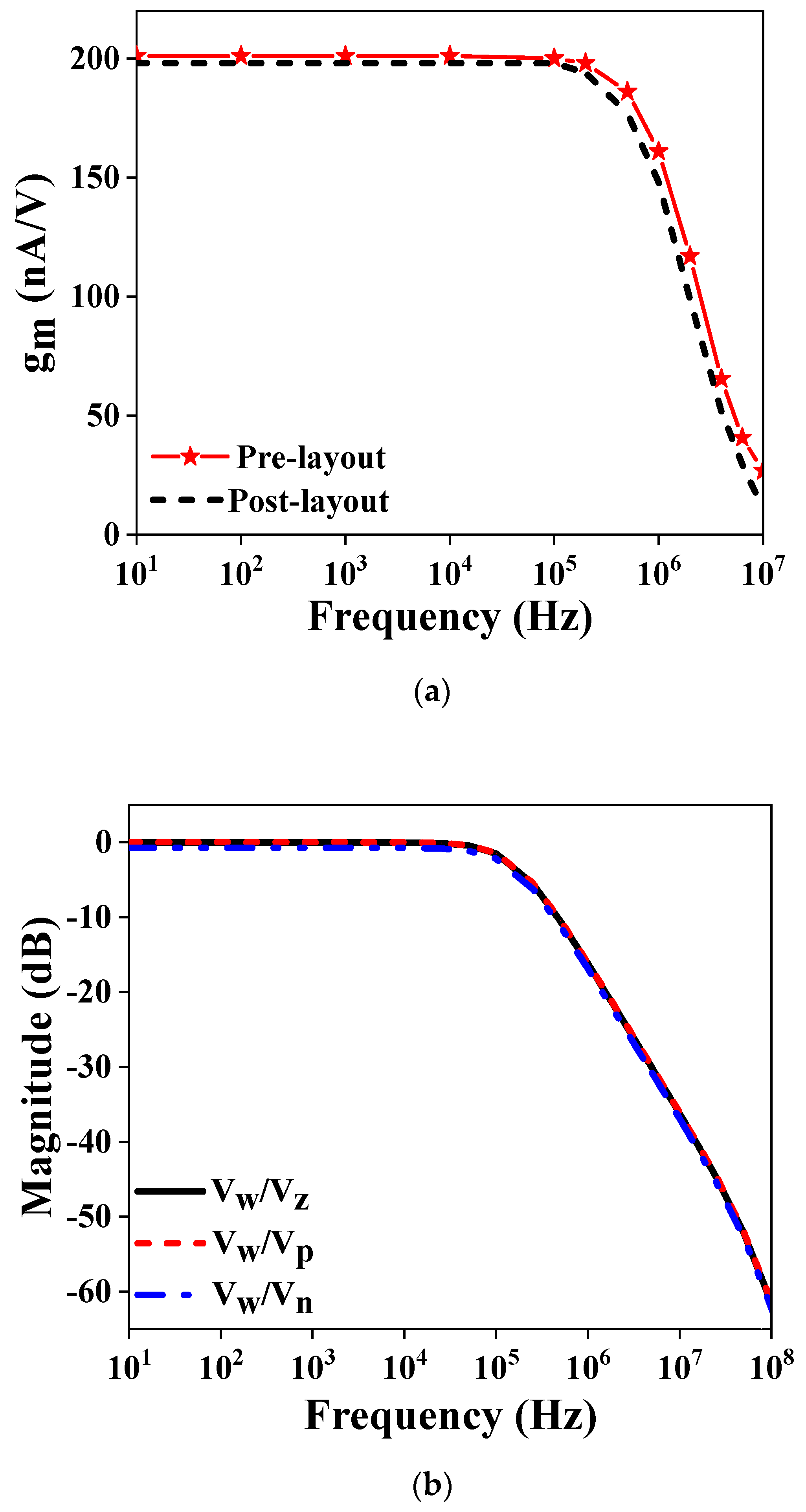
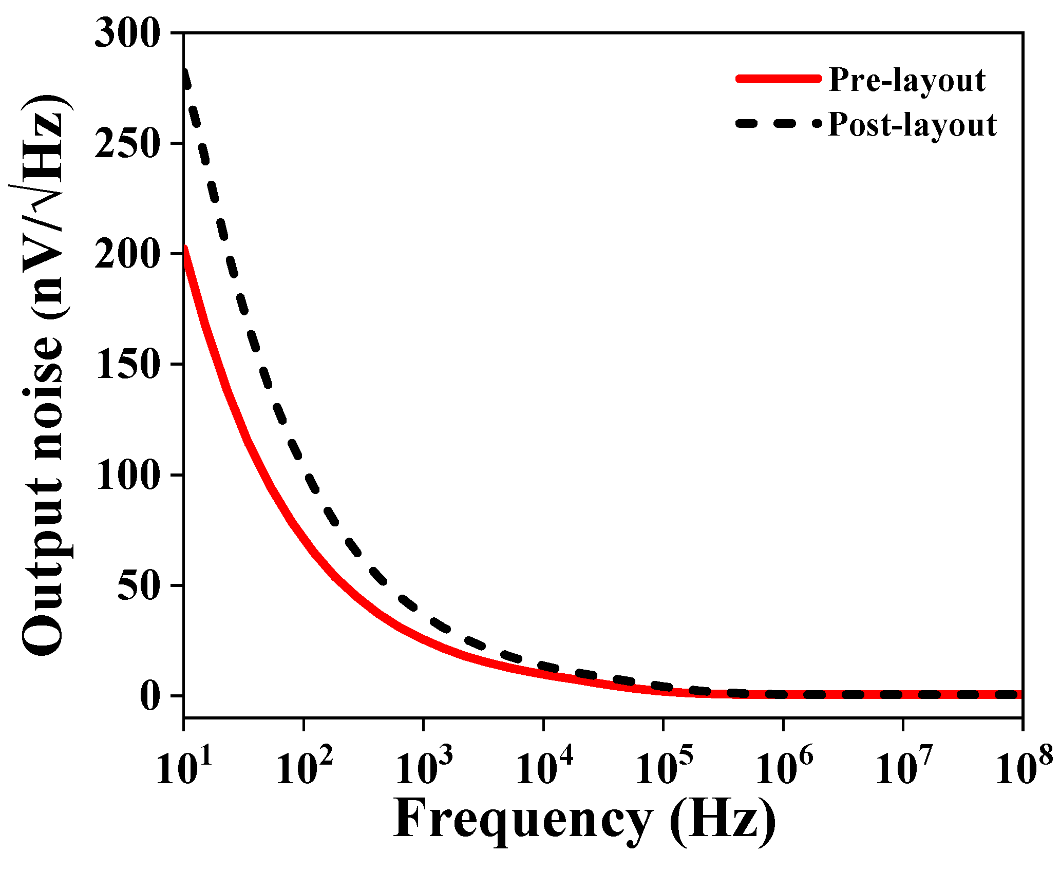
DC and AC analyses were carried out to verify the performance of VDDDA, and the corresponding simulation results are plotted in Figure 4 and Figure 5. From the DC analysis, shown in Figure 4a,b, it can be concluded that the maximum values of terminal voltages without producing significant distortion are up to ±200 mV for the OTA and −240 mV to +200 mV for the DDA, respectively. From the AC analysis shown in Figure 5a, showing pre-layout and post-layout results, it can be observed that the value of gm at a bias current (Ib) of 14 nA is approximately 200 nA/V. It can be seen that the pre-layout and post-layout results differ slightly from each other due to the impact of parasitic. Figure 5b shows the frequency response of the DDA. The value of gains at low frequency and −3 dB frequency for Vw/Vz, Vw/Vn, and Vw/Vp are found to be −9.1 mdB, 30 mdB, −718 mdB and 158 kHz, 141 kHz, 158 kHz, respectively. The power consumption of the BD-VDDDA circuit is observed to be 207 nW. Hence, a low power consumption value makes this circuit appropriate for low-power applications. The output noise of VDDDA is shown in Figure 6. It is 202 nV/ H z and 282 nV/ H z at 10 Hz for pre-layout and post-layout and after that, it follows an exponential decay and decreases to a value of 21.5 nV/ H z and 30.9 nV/ H z at 1 kHz for pre-layout and post-layout.
Another compact structure of VDDDA suitable for low-voltage applications was presented in [25]. When the proposed VDDDA was compared with the existing structure, we found that in the existing structure, 17 multiple-input gate-driven MOSFETs are being used in contrast to 19 bulk-driven MOSFETs in the proposed structure. Although the transistor count is low in the existing structure, multiple-input gate-driven MOSFETs are being used which will automatically increase the chip area and thus power dissipation as the multiple-input gate-driven MOSFETs require capacitors at their inputs. Also, the existing circuit uses a power supply of ±900 mV and the power dissipation is 0.99 mW in contrast to ±300 mV and 207 nW for the power supply and power dissipation, respectively, of the proposed circuit. So, in the context of the CMOS structure, the proposed VDDDA is a novel solution and is suitable for low-voltage and low-power applications.

3. Fractional-Order Low-Pass Filter (FO-LPF)

3.1. Basics of FO-LPF of Order 1 + α

The Laplacian operator, sα, is used to design fractional-order filters. An easy way to use sα is to use a fractance element, but despite various efforts, most of them are now still in their development stage [29,30]. Because fractance devices are commercially unavailable, physical realizations of these filters are not possible. Neverthless, using continued fraction expansions (CFEs), the obtained second-order approximation for the Laplacian operator is given below:
τ s   α = α 2 + 3 α + 2 τ 2 s 2 + 8 2 α 2 τ s + α 2 3 α + 2 α 2 3 α + 2 τ 2 s 2 + 8 2 α 2 τ s + α 2 + 3 α + 2 .
The TF of a FO-LPF of order 1 + α, where (0 < α < 1), with Butterworth characteristics and cut-off frequency ω0 = 1/τ, is given below:
H 1 + α L P s = K 1 ( τ s ) 1 + α + K 3 ( τ s ) α + K 2 .
Here, K1, K2, and K3 are constants whose values are obtained through an algorithm to achieve the required filter characteristics. Using (2), the TF of the IO low-pass filter is given by the following:
H 1 + α L P s a 2 s 2 + a 1 s + a 0 s 3 + b 2 s 2 + b 1 s + b 0 .
The values of coefficients ai (i = 0, 1, 2) and bi (i = 0, 1, 2) in (4) are given as follows:
a 2 = 1 τ α 2 3 α + 2 α 2 + 3 α + 2 K 1 ,
a 1 = 1 τ 2 8 2 α 2 α 2 + 3 α + 2 K 1 ,
a 0 = 1 τ 3 K 1 .
b 2 = 1 τ ( K 2 + K 3 2 ) α 2 3 ( K 2 K 3 ) α + ( 8 + 2 K 2 + 2 K 3 ) α 2 + 3 α + 2 ,
b 1 = 1 τ 2 ( 1 2 K 2 2 K 3 ) α 2 3 α + ( 2 + 8 K 2 + 8 K 3 ) α 2 + 3 α + 2 ,
b 0 = 1 τ 3 ( K 2 + K 3 ) α 2 3 ( K 2 K 3 ) α + 2 ( K 2 + K 3 ) α 2 + 3 α + 2 .
For the filter to have Butterworth characteristics, constants K1, K2, and K3 were derived by the computation of the cumulative error, and particularly, the values that resulted in the smallest cumulative band-pass error were utilized in [31]. K1, K2, and K3 are given by the following expressions:
K 1 = 1 ,
K 2 = 0.2937 α + 0.71216 ,
K 3 = 1.068 α 2 + 0.161 α + 0.3324.
The functional block diagram (FBD) of inverse follow-the-leader feedback (IFLF) is depicted in Figure 7. It is used to realize the IO TF of (4) [3]. Analysis of this block diagram yields the following TF:
V o u t V i n = s 2 A 2 τ 2 + s A 1 τ 2 τ 1 + 1 τ 2 τ 1 τ 0 s 3 + s 2 1 τ 2 + s 1 τ 2 τ 1 + 1 τ 2 τ 1 τ 0 .
The values of forward gain (A1, A2), and time constants (τ0, τ1, and τ2) could be computed by equating the respective coefficients in (4) and (14) while using the expressions in (5)–(13).

3.2. Proposed FO-LPF Using LV-LP VDDDA

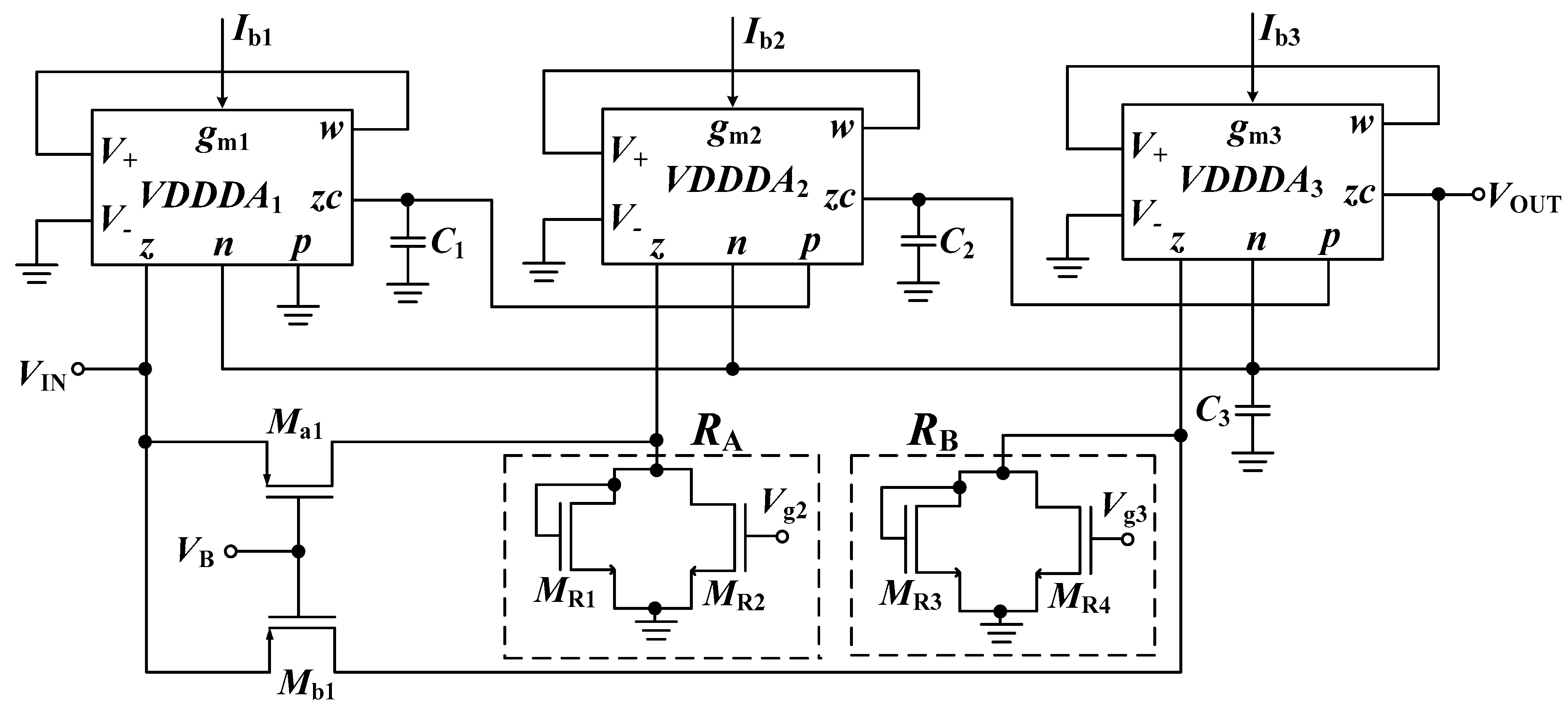
In this sub-section, the FO-LPF of order (1 + α) is implemented using the proposed BD-VDDDA. The FBD shown in Figure 7 is implemented using VDDDA as ABB. The filter implementation is shown in Figure 8. At the z-terminal of VDDDA1, an input voltage Vin is applied, while a scaled version of Vin is applied to the z-terminal of VDDDA2 and VDDDA3. These connections allow for the implementation of the forward path with gain. The output node is connected to the n-terminal of each VDDDA, implementing the feedback path. The p-terminal of VDDDA1 is connected to the ground, while the remaining p-terminals receive the signals that have been integrated by the preceding block. The integrators used in the FBD are implemented using VDDDA1–VDDDA3 along with capacitors C1 to C3. The forward paths with gains A1 and A2 are implemented using PMOS common gate amplifiers Ma1 and Mb1, where A1 = gmaRA and A2 = gmbRB. Here gma and gmb are the transconductances of transistors Ma1 and Mb1, respectively, and RA and RB are the resistances connected at the output node of Ma and Mb, respectively. In Figure 8, the implementation using transistors MR1–MR2 and MR3–MR4 represents an active resistor RA and RB, which provides a resistance value controllable through external voltages Vg2 and Vg3, respectively. Thus, this implementation provides a variable resistor whose value can be adjusted according to the required forward gain by changing the external voltages. The benefit of using active resistors in place of the physical resistor is that it reduces the chip area. Transistors MR1–MR4 are operated in the triode region, therefore the obtained grounded resistance value can be expressed as R A = 1 k n ( V g 2 2 V t n ) and R B = 1 k n ( V g 3 2 V t n ) where k n = μ n C o x W L , Vg2 and Vg3 are the externally applied voltages, and Vtn is the threshold voltage of the NMOS transistor. The TF of the FO-LPF depicted in Figure 8 is given by (9). Various parameters, such as the capacitances and transconductances values of the filter, can be calculated by equating respective coefficients in (4) and (15) along with using (5)–(13).
V O U T V I N = s 2 g m 3 A 2 C 3 + s g m 2 g m 3 A 1 C 2 C 3 + g m 1 g m 2 g m 3 C 1 C 2 C 3 s 3 + s 2 g m 3 C 3 + s g m 2 g m 3 C 2 C 3 + g m 1 g m 2 g m 3 C 1 C 2 C 3 .

3.3. Effect of Non-Idealities on FO-LPF

In this subsection, the non-ideality effect of VDDDA on the presented FO-LPF is studied. Here, two types of non-idealities are covered, i.e., non-ideality due to tracking error and parasitic. Terminal relationships in (1) are valid for the ideal VDDDA. While considering non-idealities in VDDDA, its characteristics are as follows:
I Z = g m α p V V + α n V V , V w = β z V z β n V n + β p V p .
where αp and αn are tracking errors in transconductance from V+ and V terminals to z terminal, respectively, βz, βn, and βp, are the errors in the respective voltage gain from z, n, and p terminals, respectively to the w terminal of VDDDA. Ideally, tracking errors αi and βi are considered to be unity. Taking into account the above-mentioned errors, the voltage at the zc terminal of 1st VDDDA will be as follows:
V Z C 1 = α p 1 g m 1 β Z 1 V i n β n 1 V o u t s C 1
Similarly, the voltage at the zc terminal of 2nd VDDDA is found to be as below:
V Z C 2 = α p 2 g m 2 s C 2 V i n α p 1 β Z 1 β p 2 g m 1 s C 1 + β Z 2 A 1 V o u t α p 1 β n 1 β p 2 g m 1 s C 1 + β n 2
The voltage at the w terminal of 3rd VDDDA is realized as the following:
V w 3 = V i n α p 1 α p 2 β Z 1 β p 2 β p 3 g m 1 g m 2 s 2 C 1 C 2 + α p 2 g m 2 β p 3 β Z 2 A 1 s C 2 + β Z 3 A 2 V o u t α p 1 α p 2 β n 1 β p 2 β p 3 g m 1 g m 2 s 2 C 1 C 2 + α p 2 β n 2 β p 3 g m 2 s C 2 + β n 3
Vout, which is the voltage developed at the zc terminal of 3rd VDDDA will be as follows:
V o u t = α p 3 g m 3 V w 3 s C 3
After putting the value of Vw3 in (20) and solving the equation, the TF of the filter under the parasitic effect is given by the following:
V O U T V I N = s 2 β z 3 X 1 A 2 + s β z 2 X 1 Y 1 A 1 + β z 1 X 1 Y 1 Z 1 s 3 + s 2 β n 3 X 1 + s β n 2 X 1 Y 1 + β n 1 X 1 Y 1 Z 1 .
where, αpi, βzi, βpi and βni (i = 1, 2, 3) are the errors of the ith block, X 1 = α p 3 g m 3 C 3 , Y 1 = α p 2 β p 3 g m 2 C 2 and Z 1 = α p 1 β p 2 g m 1 C 1 . Transconductance error between V+ and z terminal and voltage gain errors between z, n, p to w terminal will affect the magnitude and phase response of the filter. The shift in pole frequency and slope value in the transition band will also be observed.
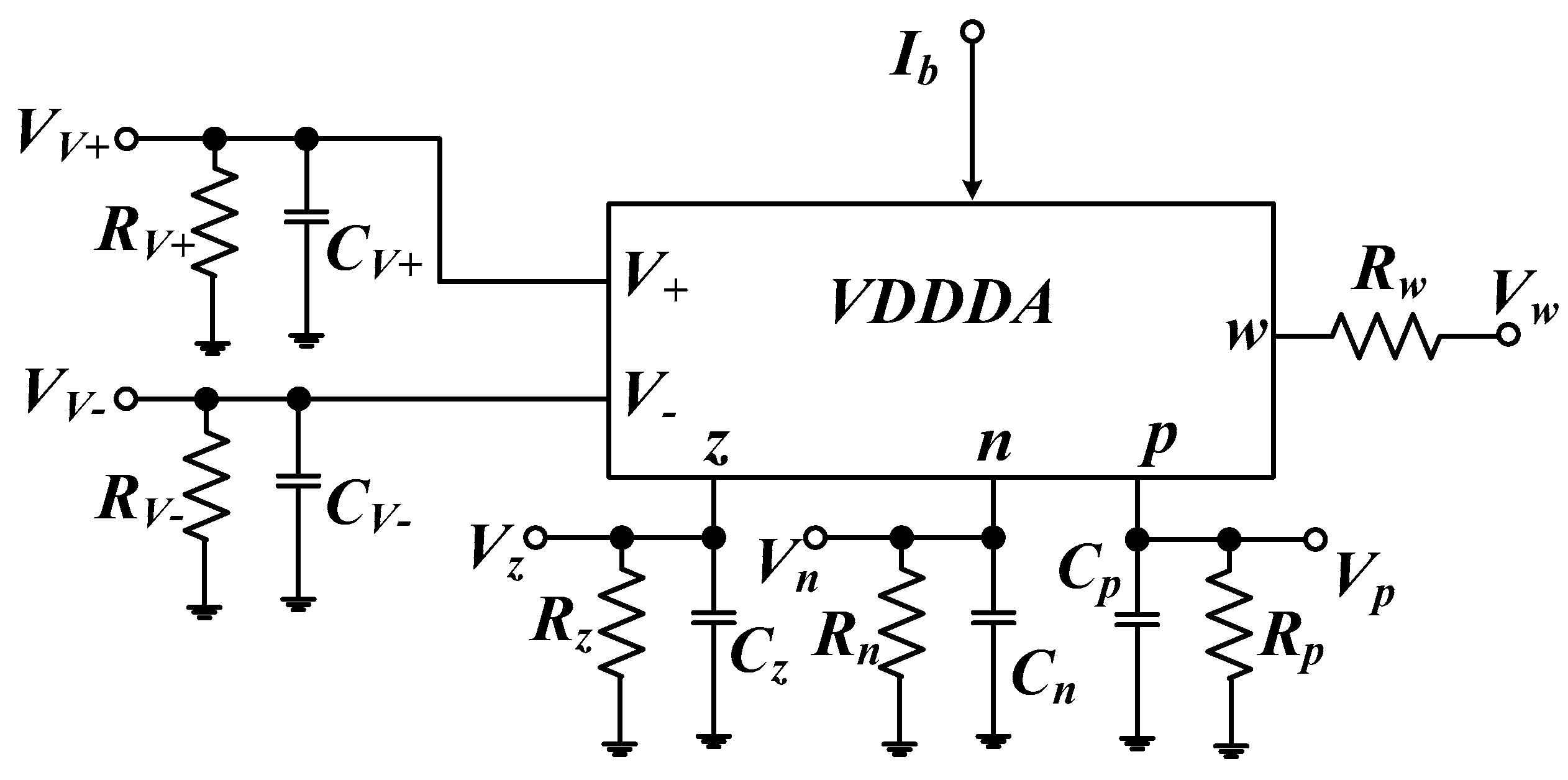
Considering the effect of parasitic impedances of VDDDA, the corresponding circuit is presented in Figure 9. The high impedance terminals V+, V, n, p, and z of VDDDA exhibit parasitic impedance in the form of shunt-connected resistances and capacitances, and at w terminal, a series resistance (Rw) is present. When considering these parasitic impedances, C T 1 = C 1 C Z C 1 C p 2 , C T 2 = C 2 C Z C 2 C p 3 , C T 3 = C 3 C Z C 3 C n 3 C n 2 C n 1 , G 1 = G Z C 1 + G p 2 ,   G 2 = G Z C 2 + G p 3   , G 3 = G Z C 3 + G n 1 + G n 2 + G n 3   ,   G Z C 1 = 1 R Z C 1 , G Z 2 = 1 R Z C 2   ,   G p 2 = 1 R p 2 , G p 3 = 1 R p 3 , G n 1 = 1 R n 1 , G n 2 = 1 R n 2 , and G n 3 = 1 R n 3 . Also, assuming A 2 * = g m B Z B   and A 1 * = g m A Z A where Z B = G B + G Z 2 , Z A = G A + G Z 3 , G B = 1 R B , G A = 1 R A , G Z 2 = 1 R Z 2 and G Z 3 = 1 R Z 3 . After analyzing the circuit, the voltage at the zc terminal of 1st VDDDA will be as follows:
V Z C 1 = g m 1 V i n V o u t s C T 1 + G 1
Similarly, the voltage at the zc terminal of 2nd VDDDA is found to be as below:
V Z C 2 = g m 2 s C T 2 + G 2 V i n g m 1 s C T 1 + G 1 + A 1 * V o u t g m 1 s C T 1 + G 1 + 1
The voltage at the w terminal of 3rd VDDDA is realized as below:
V w 3 = V i n g m 1 g m 2 s C T 1 + G 1 s C T 2 + G 2 + A 1 * g m 2 s C T 2 + G 2 + A 2 * V o u t g m 1 g m 2 s C T 1 + G 1 s C T 2 + G 2 + g m 2 s C T 2 + G 2 + 1
Vout, which is the voltage developed at the zc terminal of 3rd VDDDA will be the following:
V o u t = g m 3 V w 3 s C T 3 + G 3
After putting the value of Vw3 in (25) and solving the equation, the TF of the filter under the parasitic effect is given by the following:
V O U T V I N = s 2 A A 2 * + s A B A 1 * + A C A 2 * + A D A 2 * + G M C T + A B C A 1 * + A C D A 2 * s 3 + s 2 A + C + D + E + s A B + A C + A D + C D + C E + D E + G M C T + A B C + A C D + C D E ,
where A = g m 3 C T 3 , B = g m 2 C T 2 , C = G 1 C T 1 , D = G 2 C T 2 ,   E = G 3 C T 3 ,   G M = g m 1 g m 2 g m 3 , and C T = 1 C T 1 C T 2 C T 3 . When considering the parasitic model of VDDDA in the proposed filter, parasitic capacitances and resistances present at the terminals where a passive element is connected should be considered and may affect the magnitude and phase response of the filter at high frequency. These parasitics will also cause a shift in pole frequency and slightly change the slope value in the transition band. Nevertheless, the impact of the parasitic capacitances could be decreased by adjusting the magnitude of C1 >> CZC1 & Cp2, C2 >> CZC2 & Cp3, C3 >> CZC2, Cn3, Cn2, & Cn1, RA >> RZ2 and RB >> RZ3.

3.4. Simulation Results

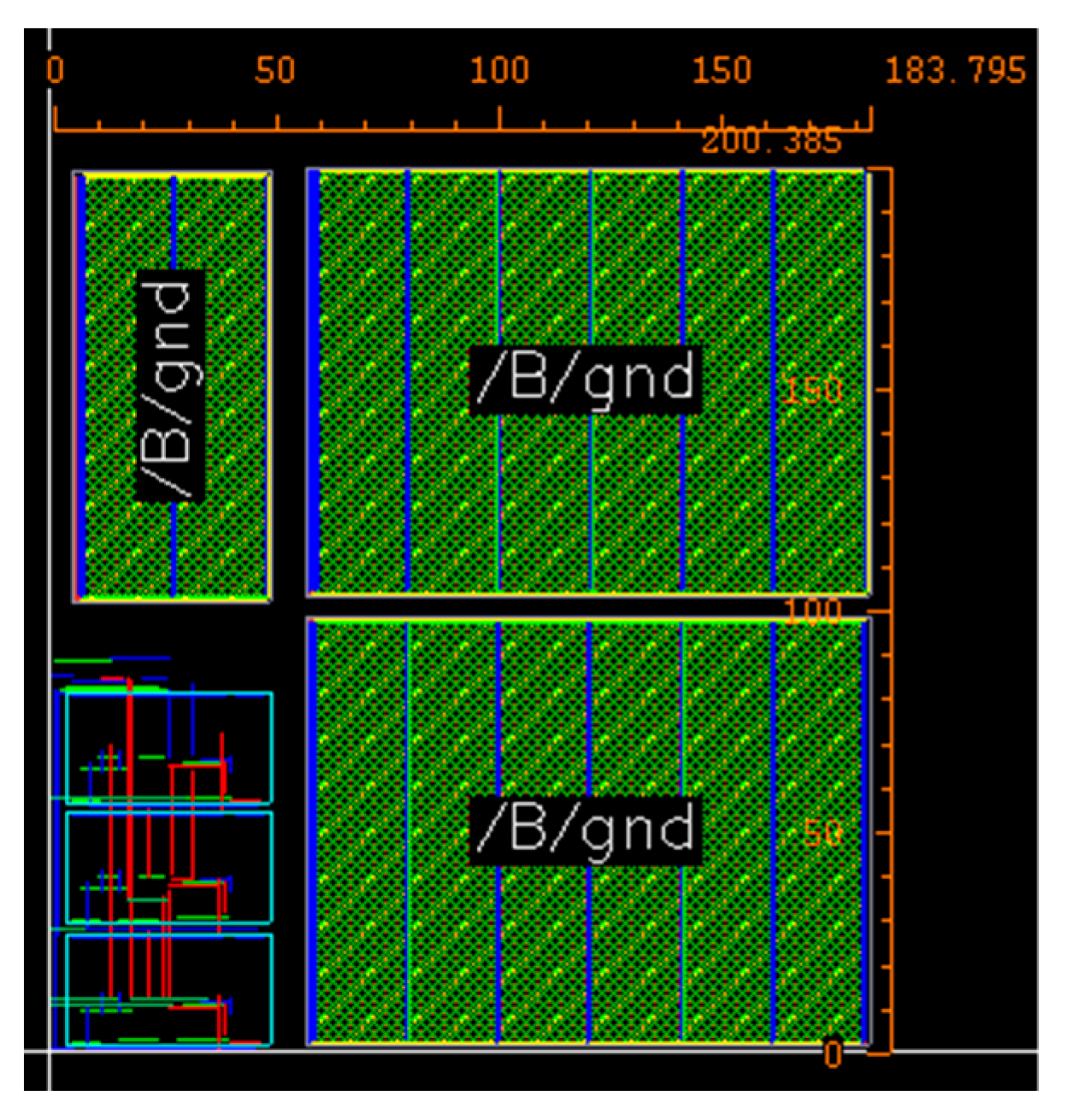
The proposed LP FO-LPF of order (1 + α), as shown in Figure 8, is simulated in the Cadence Virtuoso design tool using a 0.18 μm TSMC process parameter. The supply voltage used for filter simulation is, VDD = −VSS = 300 mV, and VB is kept at −250 mV. The layout of the proposed LV-LP fractional-order LPF circuit is shown in Figure 10. It covers an overall area of 36,600 μm2 (200.38 μm × 183.79 μm). Note that the MOS capacitor occupies a significant area in the layout. The proposed filter offers electronic tuning of its order and pole frequency by adjusting the bias current of the three VDDDAs used. Also, this electronic tuning of order and pole frequency is independent of each other. For changing the order of the filter, it is necessary to adjust the parameter α. All the parameters, such as forward gain (A1, A2), and time constants (τ0, τ1, and τ2) are dependent on the value of α. Consequently, all the transconductance values are also reliant on α. So, in order to obtain the desired transconductance value for each individual order, it is necessary to establish a distinct bias current for each VDDDA block as well as it is also necessary to change the value of resistors connected in the forward path. Figure 11 demonstrates the pre-layout and post-layout magnitude and phase response of the proposed filter, which highlights the tunability of the filter’s order. The values of capacitances, resistances, transconductances, and corresponding bias currents for different filter orders are summarized in Table 2. The bias current values are set accordingly to obtain the simulation results in Figure 11. The pole frequency selected for the simulation is 1 kHz. In Figure 11, it is evident that the attenuation in the stopband changes according to −20 × (1 + α) dB/dec, where (1 + α) is the order of the proposed filter. In Table 3, the attenuation obtained by simulation and theoretical calculation is compared for different orders. From Table 3, it is clear that the simulated result closely follows the theoretical values obtained mathematically. Also, the power consumption of the proposed FO-LPF is only 663 nW, which makes the proposed filter design suitable for the low-power application.
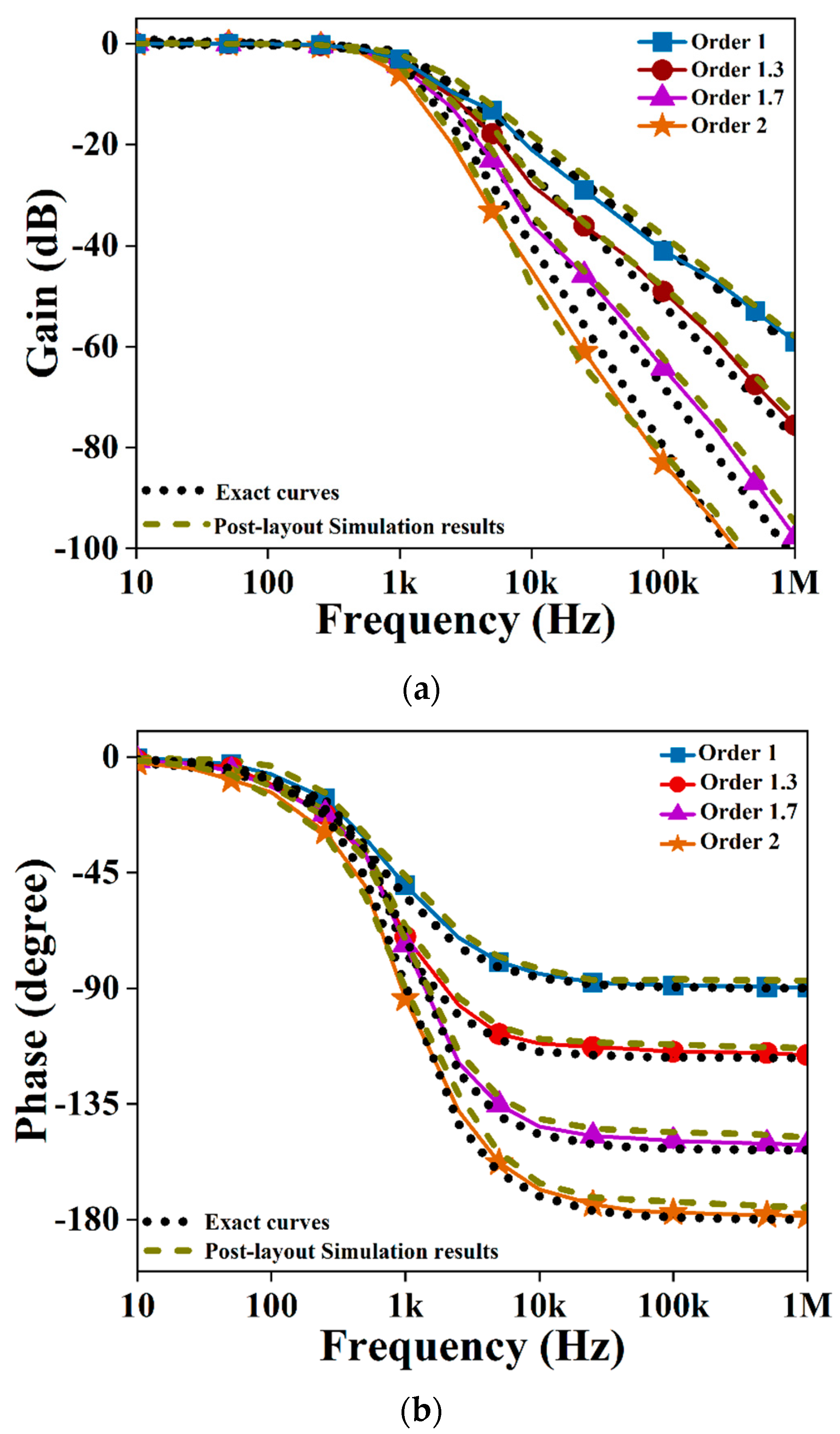
Figure 12 illustrates the magnitude and phase response of a FO-LPF for orders 1.3 and 1.7. The graphs provide a comparative analysis between the simulation results and the exact curves, as determined by (3). The resemblance between the simulated result and the exact curves is evident. The suggested filter design allows for the adjustment of the pole frequency without changing the filter’s order. This can be accomplished by modifying the transconductances of the VDDDAs that implement the integrators, while maintaining the forward current gain values as the same. In order to achieve tunability, the filter’s selected order is set to 1.5. The capacitance values, as well as the gm4 and gm5 parameters, remain unchanged from those specified in Table 2 for the purpose of this simulation. Table 4 provides a compilation of transconductances and biasing currents that were used. The simulated pre-layout and post-layout magnitude and phase response of the proposed filter showing the tunability feature for order 1.5 are shown in Figure 13. The theoretical pole frequencies chosen to illustrate the controllability are 500 Hz, 1 kHz, and 2 kHz. Pole frequency values obtained by post-layout simulations are 502 Hz, 1.003 kHz, and 2.007 kHz, which confirm the workability of the proposed design, as summarized in Table 5.
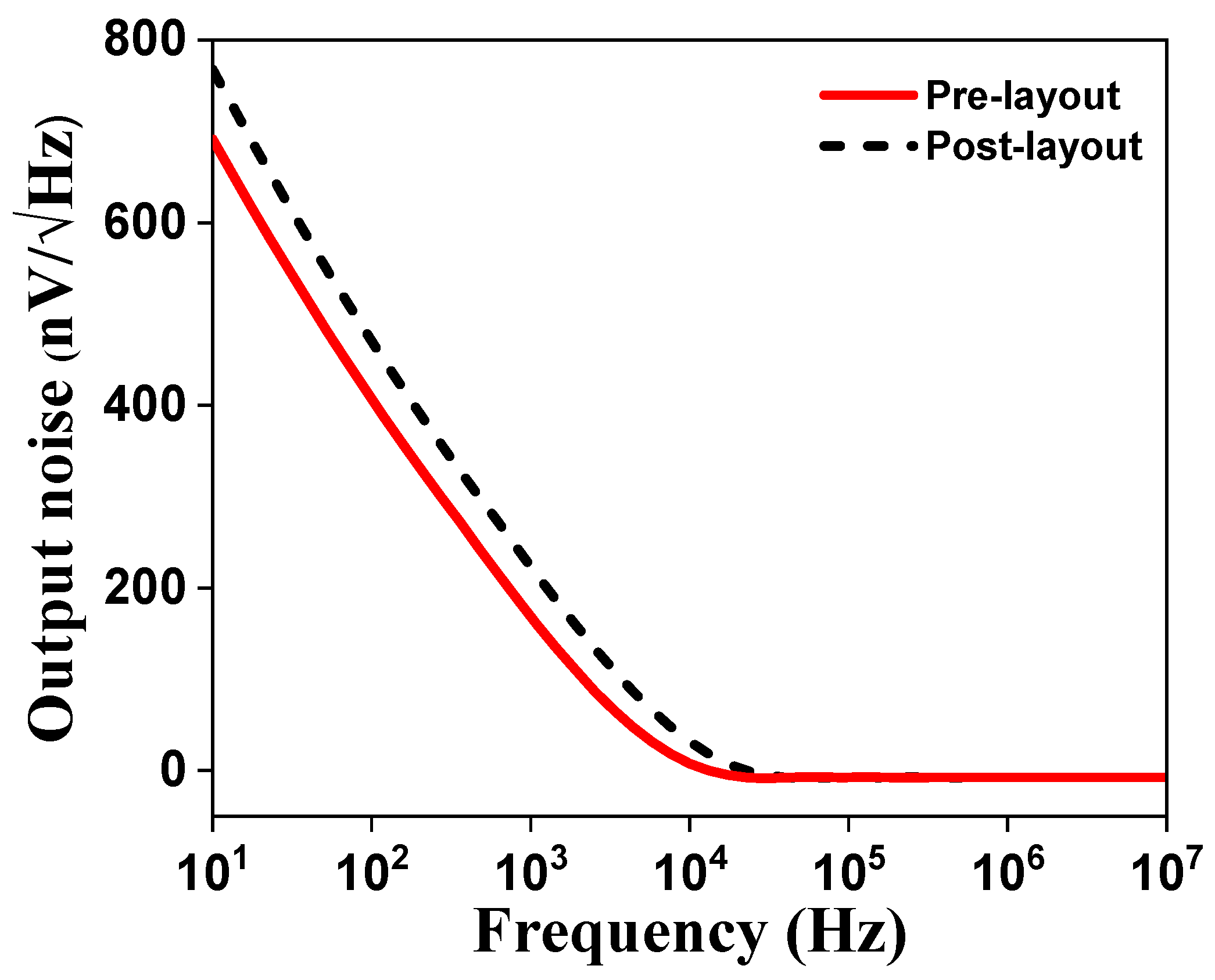
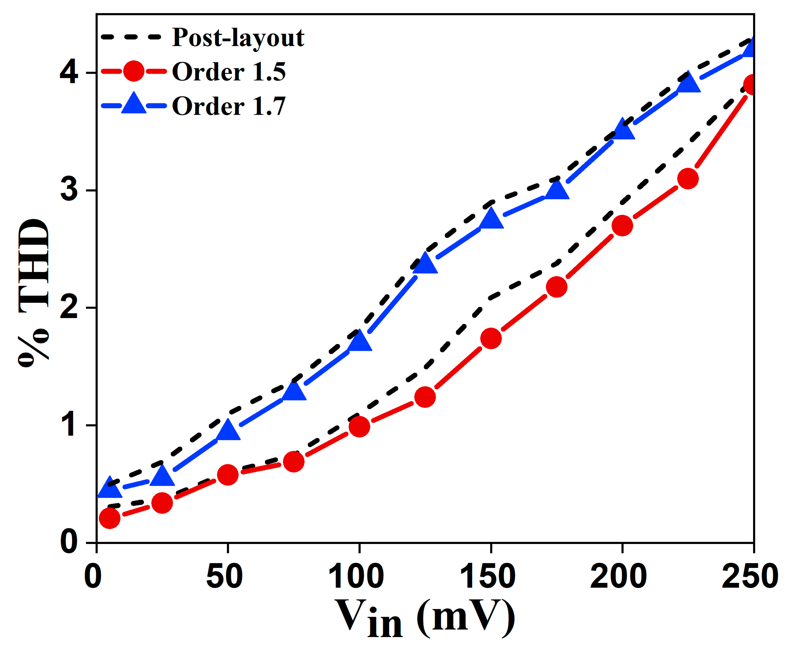
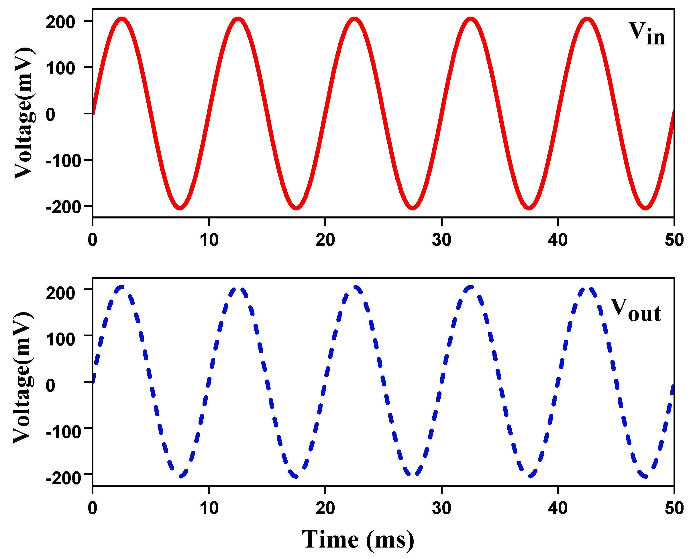
The output noise of the FO-LPF is plotted in Figure 14. The pre-layout and post-layout noise of FOF is found to be 691 nV/ Hz and 767 nV/ Hz at 10 Hz, and after that, it observes an exponential decay and decreases to a value of 134 nV/ Hz and 186 nV/ Hz at 1 kHz for pre-layout and post-layout respectively. The linear performance of the FOF for orders 1.5 and 1.7 was tested by an input signal of a single tone at 100 Hz with variable amplitude. The total harmonic distortion (THD) results are displayed in Figure 15. It is apparent that up to 250 mV of input amplitude, the THD value is below 4%, which is quite low. In Figure 16, the time domain response of FO-LPF is presented for voltage signals having amplitude of 200 mV and frequency of 100 Hz.
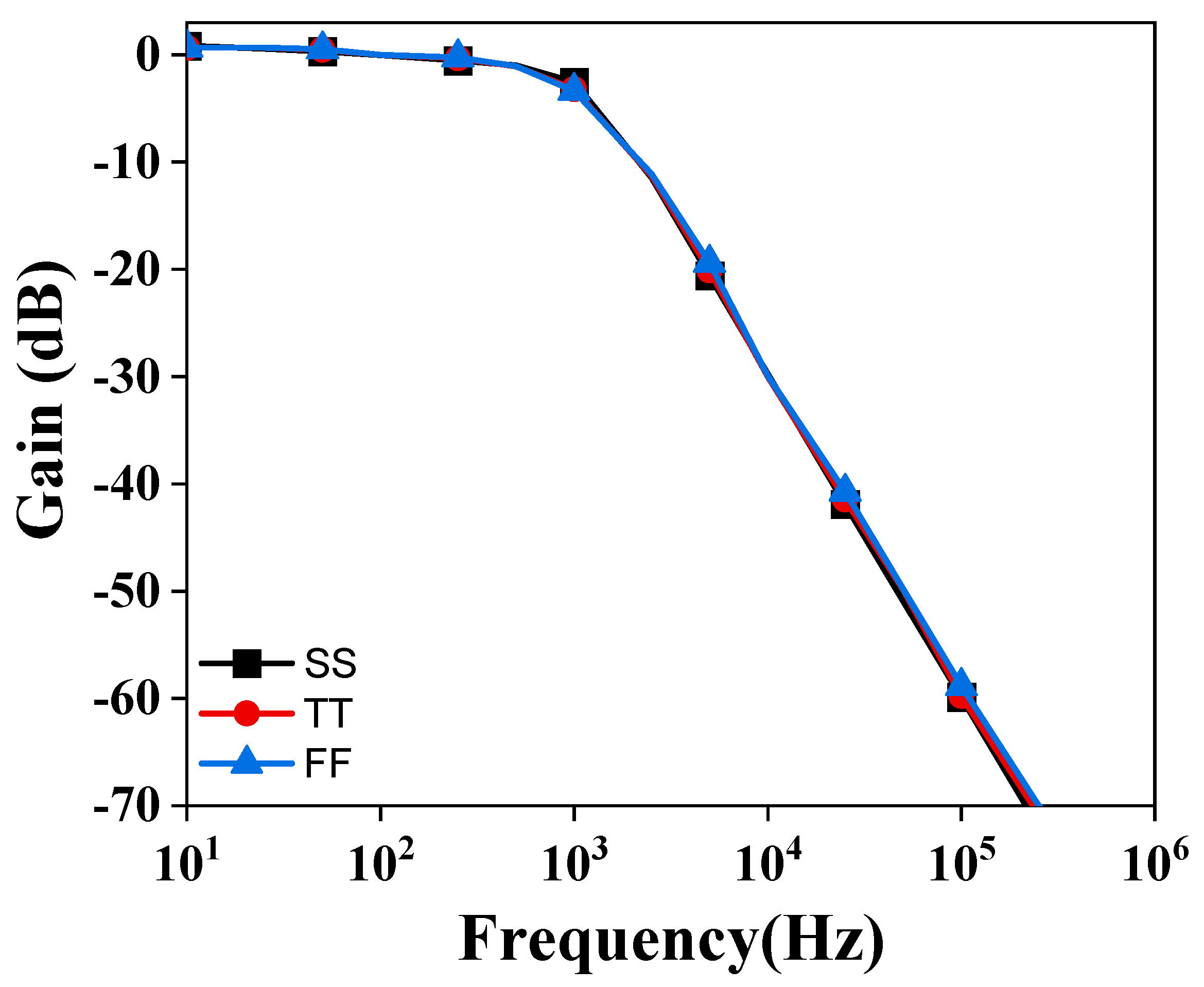
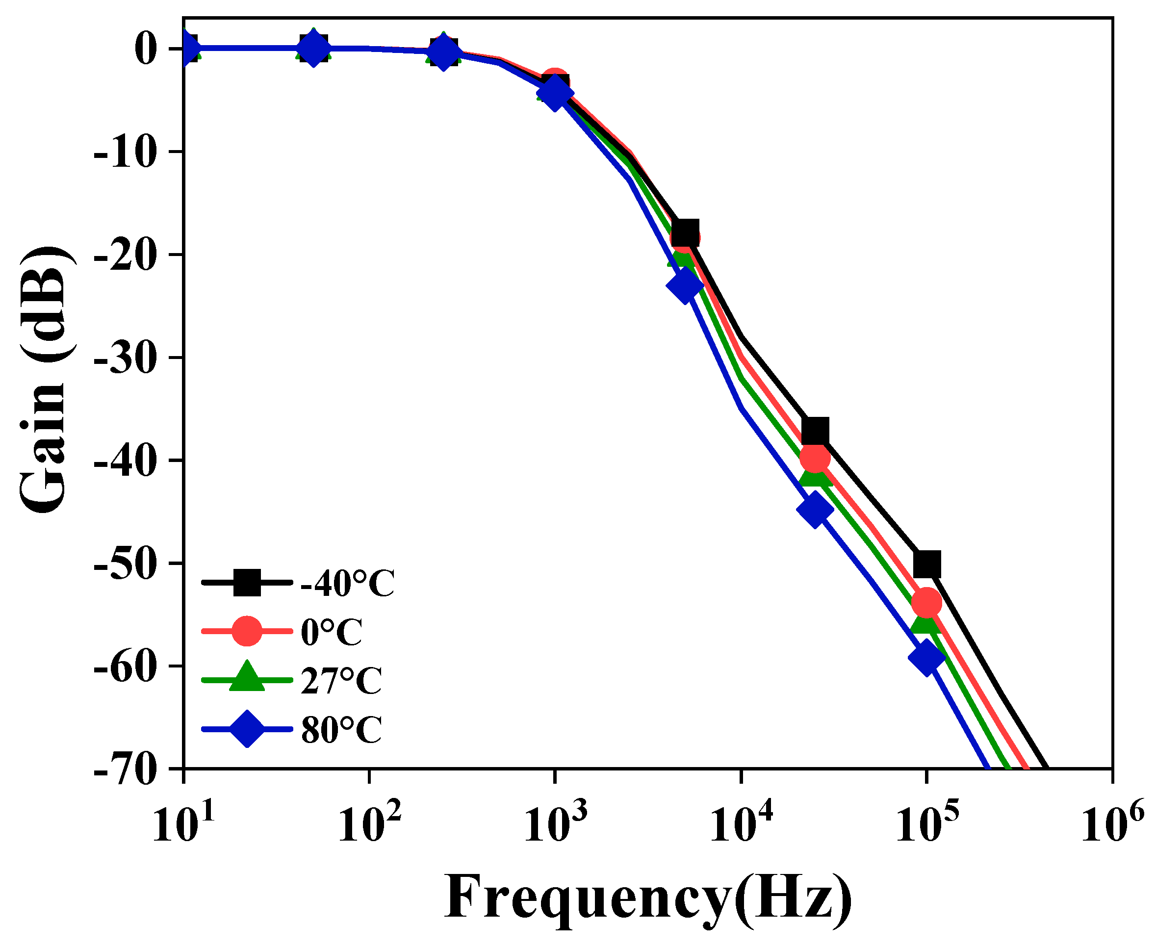
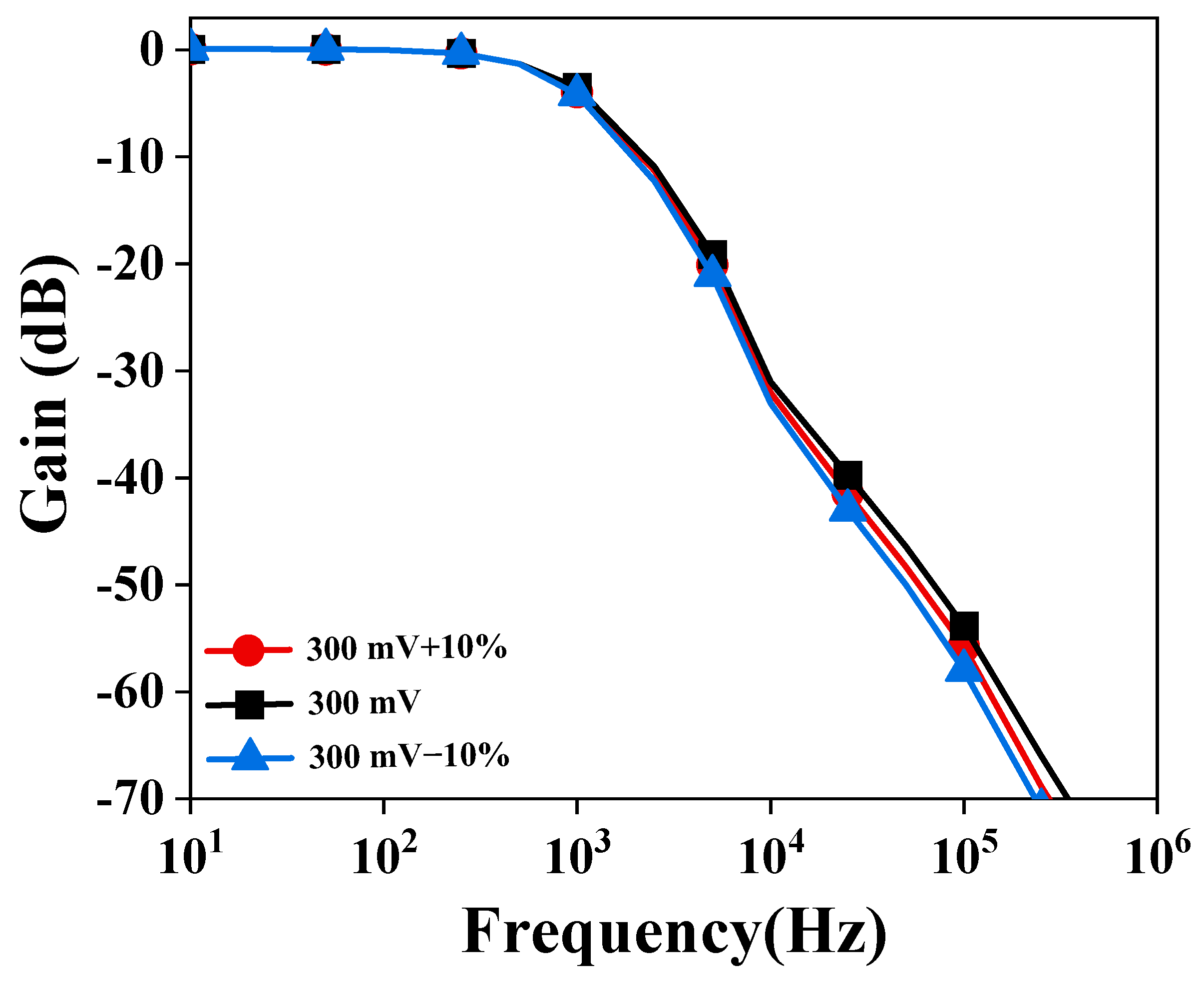
Transistor corners as SS, TT, and FF, voltage supply corners as ±10% of VDD, and temperature corners as −40 °C, 0 °C, 27 °C, and 80 °C were used in the analysis of process, voltage and temperature (PVT) corners. Figure 17, Figure 18 and Figure 19 display the outcomes of the proposed filter’s magnitude characteristics with process, voltage, and temperature corner analysis, respectively. From Figure 17, it is clear that as anticipated, the response of the process corner exhibits limited variation. Based on the magnitude curve illustrated in Figure 18, it can be inferred that the FO-LPF design does not exhibit significant variations across different temperatures. Thus, the proposed circuit demonstrates satisfactory performance throughout a broad spectrum of temperature variations. From Figure 19, FO-LPF characteristics are satisfactory for up to 10% variation in VDD. Through the use of the Monte-Carlo analysis for N = 600 samples, the sensitivity of the pole frequency with regard to the impact of transistor mismatching and process parameter fluctuations was assessed. The magnitude characteristics and statistical plots, obtained at α = 0.5, are shown in Figure 20. The standard deviation of the pole frequency is 12.94 Hz. Given that the desired pole frequency value is 1 kHz, it is possible to draw the conclusion that the filter has acceptable sensitivity characteristics.
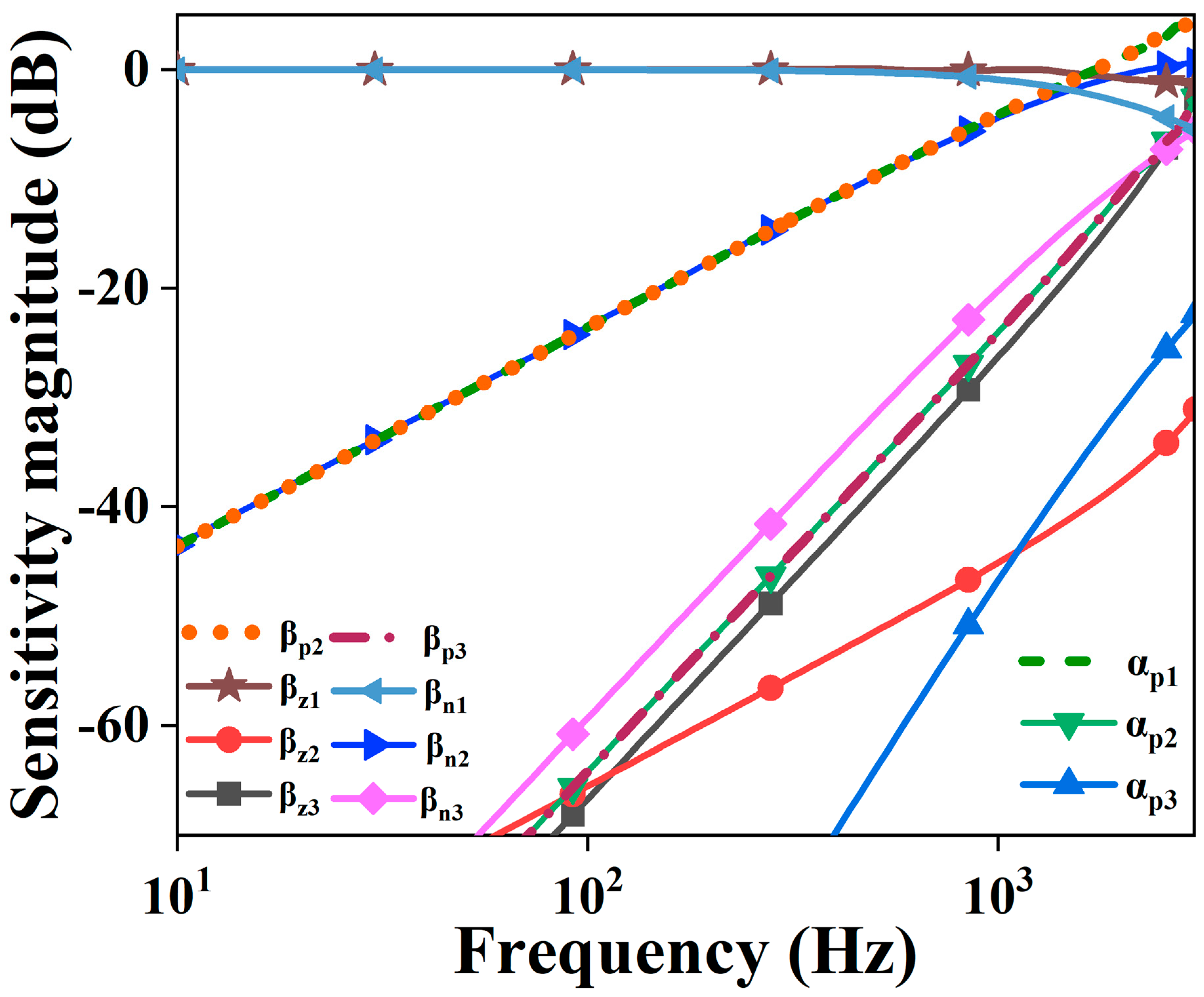
The transfer function given in (21) represents filter characteristics when the filter is affected by tracking-error parameters. To observe the effect to these parameters, the sensitivity analysis was performed for the obtained transfer function in (21), with respect to the tracking-error parameters. The objective of sensitivity analysis is to assess the impact of changes in these parameters on the performance of the filter. The given expression comprises a total of eleven tracking-error parameters that are αp1, αp2, αp3, βz1, βz2, βz3, βn1, βn2, βn3, βp2, and βp3. Through simulation, there values were obtained as follows: αp = 0.98, βz = 0.99, βn = 1.003, βp = 0.92. Generally speaking, the relative sensitivity to each parameter is characterized as follows:
S x T F = x T F d T F d x
where, TF represents the transfer function of the filter and x represents the parameter that affects this transfer function. This analysis was conducted for order 1.5 at f0 = 1 kHz. The remaining parameter values, such as capacitance, resistance, and transconductance are presented in Table 2. The sensitivity obtained for these tracking-error parameters were a function of parameter values and frequency and thus the magnitude of sensitivity versus frequency curve, in terms of the aforementioned tracking-error parameters, is depicted in Figure 21. The graph demonstrates the variation in sensitivity as a function of frequency and parameters βn1, and βz1 show highest sensitivity in the pass band range of FO-LPF.
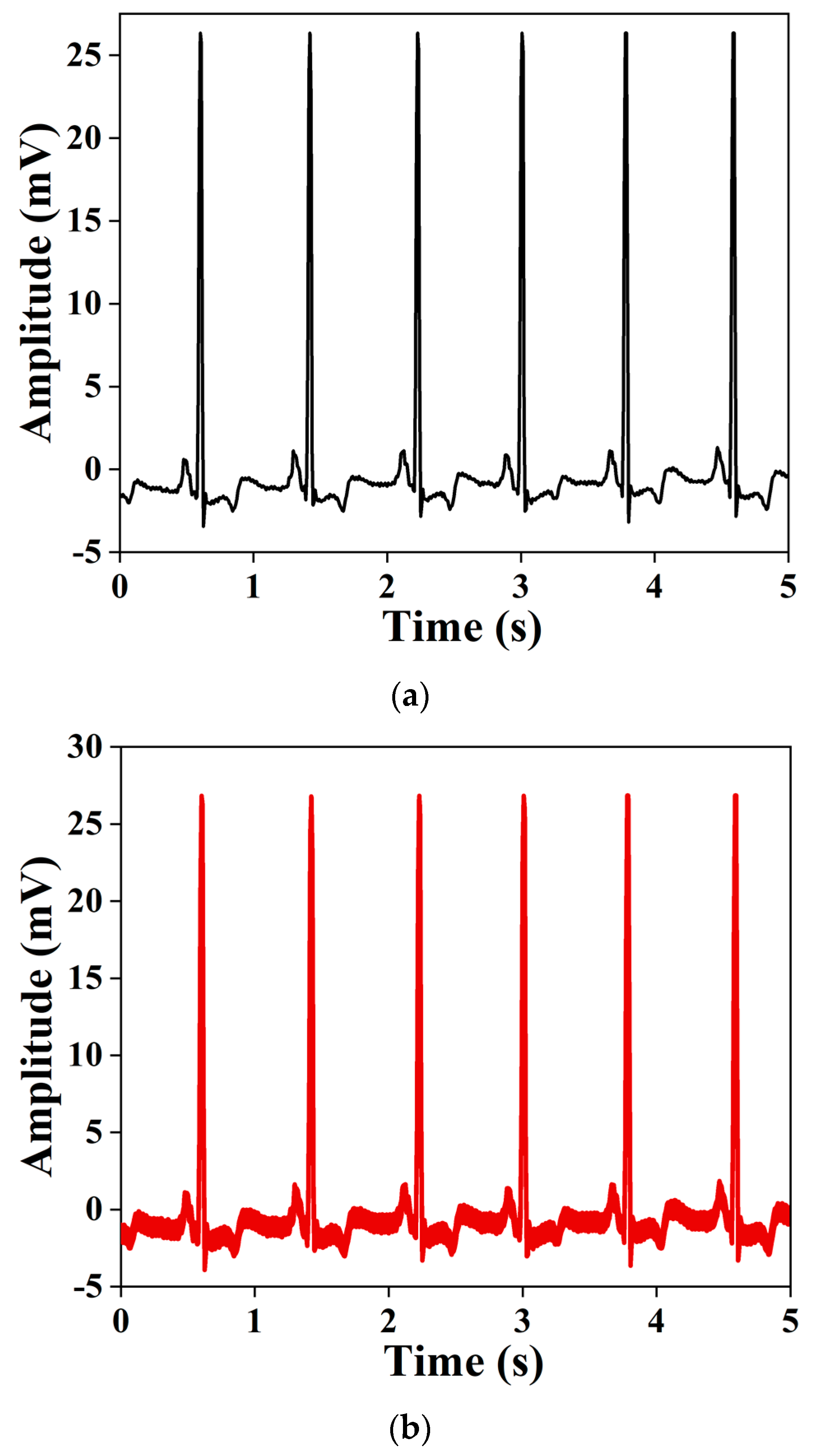
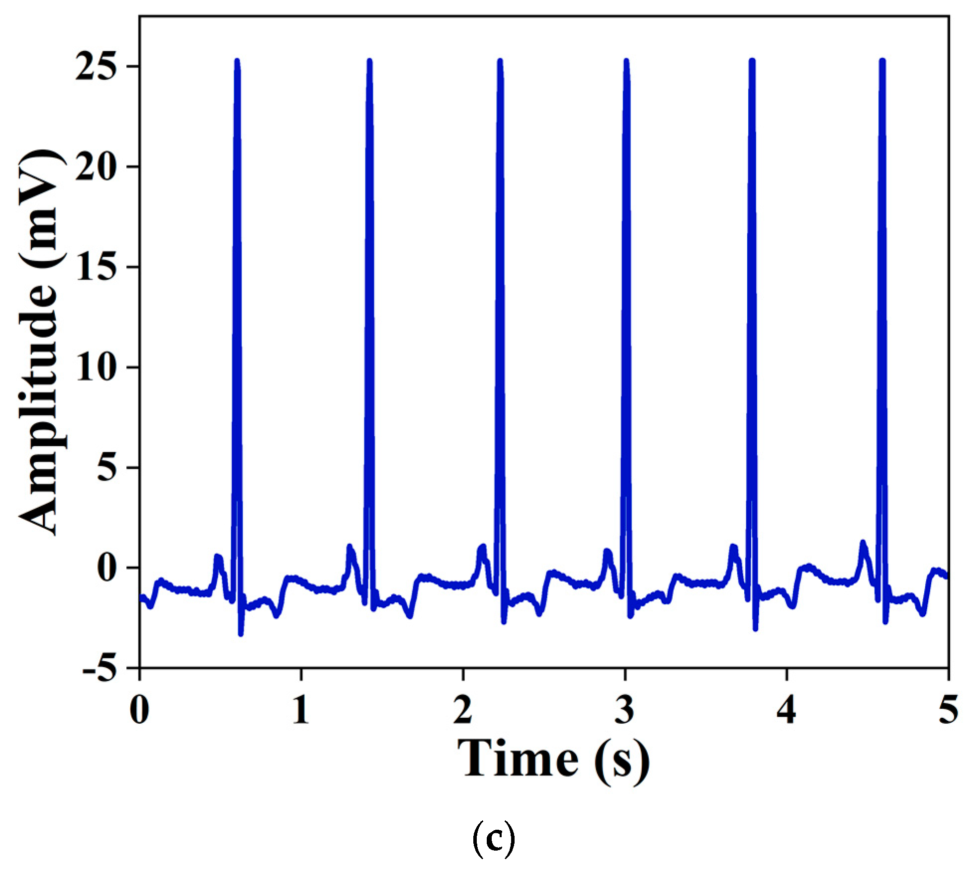
To demonstrate the practical significance of the proposed circuit, an assessment of the filter’s efficiency in processing the electrocardiogram (ECG) signal is performed. The input ECG signal exhibits an amplitude of 25 mV, and it was mixed with a sinusoidal signal of 1 kHz frequency and an amplitude of 50 μV. The noisy ECG signal was passed through the FO-LPF of pole frequency 2 kHz. Figure 22 displays the actual ECG, the ECG with added noise, and the ECG that was restored after passing through the filter. This demonstrates that the suggested filter is well-suited for practical applications such as ECG filtering.

4. Comparison

Given that the integer-order approximation technique is utilized for designing FO-LPF, the state-of-the-art in Table 6 incorporates FOFs that are designed using the same approximation technique. While comparing the proposed FOF with other FOFs available in the literature, several observations were made as outlined below.
The table reveals that the number of active blocks employed in the references [6,15,16,17,18,19,20,21,32,33,34,35,36,37] exceeds the number of blocks utilized in the proposed FOF. Additionally, the implementation of the FOF in [6,14,15,16,19,20,21,32,33,36,37] involves the utilization of a significant quantity of resistors. It is worth noting that the majority of these resistors are floating. Conversely, the proposed FOF incorporates a grounded active resistor that is implemented using MOSFET, making the design well-suited for the fabrication process. In addition, it should be noted that the designs, with the exception of the ones referenced as [17,18,32,33,34,36,37], do not offer tunability of order and pole frequency.
Regarding the utilization of passive components, it is seen that only [17,18,34,35] exhibit an equivalent or lesser quantity of passive components compared to the design under consideration. However, upon analysing the number of active components, it is evident that [17,18,34,35] exhibit a significantly greater number of active components in comparison to the proposed design. Additionally, the design of [35] incorporates the utilization of five fractional capacitors (FC). The functions performed by [20,34,36] encompass LPF along with additional functionalities. However, [20] employs floating passive components and lacks electronic tuning capabilities. On the other hand, [34] utilizes a significant number of active components, operates at a higher supply voltage, and exhibits high power dissipation. Ref. [36] employs floating passive components and incorporates five FCs in its design. The DC supply voltage employed for the operation of the suggested filter circuit is ±300 mV, which is the smallest value when compared to the other designs. It is comparable only to [19], where the supply voltage is ±0.5 V. However, it should be noted that [19] utilizes resistors in the implementation of the filter. The LV-LP methodology is utilized in the filter implementation only in [19] and the proposed method. Consequently, none of the other circuits can be considered suitable for operation in the LV-LP domain. Furthermore, the power consumption of the suggested circuit is the lowest among the designs that were studied.
Thus, the proposed circuit is beneficial in terms of its use of only three active building blocks, six MOS transistors, and three grounded capacitors for implementing fractional-order LPF, which is suitable for its operation in the LV-LP domain since it uses only ±300 mV as its power supply and consumes only 663 nW. The proposed filter offers electronic and independent order and pole frequency tuning. Furthermore, this is the only circuit apart from [19] to be used in the low-voltage and low-power domain.

5. Conclusions

In this paper, a VDDDA and a low-pass fractional-order filter structure capable of operating at low voltage and in low-power applications were presented. The VDDDA structure is implemented using the bulk-driven metal oxide semiconductor (BD-MOS) transistor technique and is operated in the subthreshold region. VDDDA uses VDD = −VSS = 300 mV and dissipates only 207 nW of power for its operation. Furthermore, this block is used to implement a FO-LPF of order (1 + α). The filter structure comprises three VDDDAs, three grounded capacitors, and two active resistors. Also, the electronic tuning feature of the proposed filter design offers independent tuning of its order and frequency through the bias current of the active component used. The effects of tracking errors and parasitics on the performance of the proposed FO-LPF were analyzed. This filter is capable of LV-LP operation because it is operated at ±300 mV and dissipates only 663 nW of power. The layout of the proposed VDDDA, as well as the FO-LPF, were laid out in a Cadence environment using 0.18 μm CMOS technology parameters and covered a chip area of 1208 μm2 and 36,600 μm2, respectively. Post-layout simulation results are also included, which imply that they are suitable for fabrication. Noise, total harmonic distortion, Monte-Carlo and PVT analyses were also performed.

Author Contributions

Conceptualization, S.T. and R.K.R.; methodology, S.T.; software, S.T.; validation, S.T., R.K.R., and S.K.P.; formal analysis, S.K.P.; investigation, N.H.; resources, R.K.R.; data curation, S.T.; writing—original draft preparation, S.T., R.K.R., S.K.P., and N.H.; writing—review and editing, S.T., R.K.R., S.K.P., and N.H.; visualization, S.K.P. and N.H.; supervision, R.K.R.; project administration, N.H.; funding acquisition, N.H. All authors have read and agreed to the published version of the manuscript.

Funding

This work was supported in part by the Department of Electronics Engineering, IIT (ISM), India, through Projects SICRG, under Grant MHRD [Shastri Institutional Collaborative Research Grant (SICRG)]/2020-2021/740/ECE, MeitY (Ministry of Electronics and Information Technology) under Grant MietY/2023-2024/1012/ECE entitled “Ultra-Low Power Neuromorphic Spiking Architecture for Assistive Smart Glass” and CSIR under Grant Project no 70/0081/23/EMR-II entitled “Memristor Based Multilayer Neural Networks (MNN) and its application in Neuromorphic System”.

Data Availability Statement

The data presented in this study are available upon request from the corresponding author.

Conflicts of Interest

The authors declare no conflict of interest.

Appendix A

The drain current of a long-channel PMOS transistor operating in a weak inversion region is given by [38]:
I o u t = I s W L e V S G V t h n V T 1 e V S D V T .
where I s = 2 n V T 2 × μ C o x , VT is the thermal voltage having a value of 25 mV at room temperature, and n is the slope factor. If VSD > 3VT, then input transistors are in the saturation region of weak inversion. By considering Vth = VTO − (n − 1) VSB and VSD > 3VT, (A1) is simplified to the following:
I o u t = I s W L e V S G V T 0 + ( n 1 ) V S B n V T .  
Since, Iout = IZ = ID1ID2, using values of ID1 and ID2 from (A2), Iout can be written as below:
I o u t = I s W L e V S G 1 V T 0 + ( n 1 ) V S B 1 n V T e V S G 2 V T 0 + ( n 1 ) V S B 2 n V T ,
I o u t = I s W L e V T 0 / n V T e V S G 1 + ( n 1 ) V S B 1 n V T α e V S G 2 + ( n 1 ) V S B 2 n V T β .
Multiplying the above equation by α + β α + β , and then assuming Ix = ID1 + ID2, (A3) can be rewritten as follows:
I o u t = I X e V S G 1 V S G 2 + ( n 1 ) V S B 1 V S B 2 2 n V T e V S G 2 V S G 1 + ( n 1 ) V S B 2 V S B 1 2 n V T e V S G 1 V S G 2 + ( n 1 ) V S B 1 V S B 2 2 n V T + e V S G 2 V S G 1 + ( n 1 ) V S B 2 V S B 1 2 n V T .
Now, from Figure 2, we deduce the following:
VSG1 = VS1VG, VSG2 = VS2VG, VSB1 = VS1V+, VSB2 = VS2V
Now, putting these values in (A4), and using t a n h ( x ) = e x e x e x + e x , (4) can be simplified as follows:
I o u t = I X t a n h ( n 1 ) V + V 2 n V T ,
I o u t = I B t a n h ( n 1 ) V i n 2 n V T .
Using Taylor series expansion, (A5) can be decomposed and considering (n − 1) = η, the transconductance of the input differential pair can be given as below:
G m = I o u t V i n = I B ( n 1 ) 2 n V T = n 1 I B 2 n V T = n 1 g m 1,2 ,
G m = g m b 1,2 .

References

  1. Shah, D.K.; Chaurasiya, R.B.; Vyawahare, V.A.; Pichhode, K.; Patil, M.D. FPGA implementation of fractional-order chaotic systems. AEU-Int. J. Electron. Commun. 2017, 78, 245–257. [Google Scholar] [CrossRef]
  2. Elsafty, A.H.; Tolba, M.F.; Said, L.A.; Madian, A.H.; Radwan, A.G. Enhanced hardware implementation of a mixed-order nonlinear chaotic system and speech encryption application. AEU-Int. J. Electron. Commun. 2020, 125, 153347. [Google Scholar] [CrossRef]
  3. Radwan, A.G.; Khanday, F.A.; Said, L.A. (Eds.) Fractional-Order Design: Devices, Circuits, and Systems; Academic Press: Amsterdam, The Netherlands; Elsevier Science: Amsterdam, The Netherlands, 2021. [Google Scholar]
  4. Rezazadehshabilouyoliya, V.; Atasoyu, M.; Ozoguz, S. Emulation of a constant phase element by utilizing a lattice structure based fractional-order differentiator. AEU-Int. J. Electron. Commun. 2020, 127, 153418. [Google Scholar] [CrossRef]
  5. Elwakil, A.S. Fractional-order circuits and systems: An emerging interdisciplinary research area. IEEE Circuits Syst. Mag. 2010, 10, 40–50. [Google Scholar] [CrossRef]
  6. Koton, J.; Sladok, O.; Salasek, J.; Ushakov, P.A. Current-mode fractional low-and high-pass filters using current conveyors. In Proceedings of the 8th International Congress on Ultra-Modern Telecommunications and Control Systems and Workshops (ICUMT), Lisbon, Portugal, 18–20 October 2016. [Google Scholar]
  7. Valsa, J.; Dvorak, P.; Friedl, M. Network model of the CPE. Radioengineering 2011, 20, 619–626. [Google Scholar]
  8. Adhikary, A.; Sen, S.; Biswas, K. Practical realization of tunable fractional order parallel resonator and fractional order filters. IEEE Trans. Circuits Syst. I Reg. Pap. 2016, 63, 1142–1151. [Google Scholar] [CrossRef]
  9. Abdelaty, A.M.; Soltan, A.; Ahmed, W.A.; Radwan, A.G. Fractional order Chebyshev-like low-pass filters based on integer order poles. Microelectron. J. 2019, 90, 72–81. [Google Scholar] [CrossRef]
  10. Khalil, N.A.; Said, L.A.; Radwan, A.G.; Soliman, A.M. Generalized two-port network based fractional order filters. AEU-Int. J. Electron. Commun. 2019, 104, 128–146. [Google Scholar] [CrossRef]
  11. Varshney, G.; Pandey, N.; Pandey, R. Electronically tunable multifunction transadmittance-mode fractional-order filter. Arabian J. Sci. Eng. 2021, 46, 1067–1078. [Google Scholar] [CrossRef]
  12. Mishra, S.K.; Gupta, M.; Upadhyay, D.K. Active realization of fractional order Butterworth lowpass filter using DVCC. J. King Saud Univ. Eng. Sci. 2020, 32, 158–165. [Google Scholar] [CrossRef]
  13. Ghoneim, M.; Hesham, R.; Yassin, H.; Madian, A. α-order universal filter realization based on single input multi-output differential voltage current conveyor. Analog Integr. Circuits Signal Process. 2021, 107, 411–422. [Google Scholar] [CrossRef]
  14. Maundy, B.; Elwakil, A.S.; Freeborn, T.J. On the practical realization of higher-order filters with fractional stepping. Signal Process. 2011, 91, 484–491. [Google Scholar] [CrossRef]
  15. Verma, R.; Pandey, N.; Pandey, R. CFOA based low pass and high pass fractional step filter realizations. AEU-Int. J. Electron. Commun. 2019, 99, 161–176. [Google Scholar] [CrossRef]
  16. Tsirimokou, G.; Koumousi, S.; Psychalinos, C. Design of fractional-order filters using current feedback operational amplifiers. J. Eng. Sci. Technol. Rev. 2016, 9, 71–81. [Google Scholar] [CrossRef]
  17. Langhammer, L.; Dvorak, J.; Jerabek, J.; Koton, J.; Sotner, R. Fractional-order high-pass filter with electronically adjustable parameters. J. Electr. Eng. 2018, 69, 3–13. [Google Scholar]
  18. Jerabek, J.; Sotner, R.; Dvorak, J.; Polak, J.; Kubanek, D.; Herencsar, N.; Koton, J. Reconfigurable fractional-order filter with electronically controllable slope of attenuation, pole frequency and type of approximation. J. Circuits Syst. Comput. 2017, 26, 1750157. [Google Scholar] [CrossRef]
  19. Khateb, F.; Kubánek, D.; Tsirimokou, G.; Psychalinos, C. Fractional-order filters based on low-voltage DDCCs. Microelectron. J. 2016, 50, 50–59. [Google Scholar] [CrossRef]
  20. Kaur, G.; Ansari, A.Q.; Hashmi, M.S. Analysis and investigation of CDBA based fractional-order filters. Analog Integr. Circuits Signal Process. 2020, 105, 111–124. [Google Scholar] [CrossRef]
  21. Koton, J.; Kubanek, D.; Sladok, O.; Vrba, K.; Shadrin, A.; Ushakov, P. Fractional-order low-and high-pass filters using UVCs. J. Circuits Syst. Comput. 2017, 26, 1750192. [Google Scholar] [CrossRef]
  22. Herencsar, N.; Sotner, R.; Metin, B.; Koton, J.; Vrba, K. VDDDA-New ‘voltage differencing’ device for analog signal processing. In Proceedings of the 8th International Conference on Electrical and Electronics Engineering (ELECO), Bursa, Turkey, 28–30 November 2013. [Google Scholar]
  23. Soisang, S.; Jirasereemomkul, K.; Jaikla, W.; Higuchi, K. Voltage-mode multifunctional biquadratic filter using VDDDA. Appl. Mech. Mater. 2015, 781, 155–159. [Google Scholar] [CrossRef]
  24. Sangyaem, S.; Siripongdee, S.; Jaikla, W.; Khateb, F. Five-inputs single-output voltage mode universal filter with high input and low output impedance using VDDDAs. Optik 2017, 128, 14–25. [Google Scholar] [CrossRef]
  25. Jaikla, W.; Khateb, F.; Kulej, T.; Pitaksuttayaprot, K. Universal filter based on compact CMOS structure of VDDDA. Sensors 2021, 21, 1683. [Google Scholar] [CrossRef] [PubMed]
  26. Alagoz, B.B.; Yeroglu, C.; Kavuran, G.; Ates, A. Detection of RR interval alterations in ECG signals by using first order fractional filter. In Proceedings of the 39th International Conference on Telecommunications and Signal Processing (TSP), Vienna, Austria, 27–29 June 2016. [Google Scholar]
  27. Kulej, T.; Khateb, F.; Kumngern, M. 0.3-V nanopower biopotential low-pass filter. IEEE Access 2020, 8, 119586–119593. [Google Scholar] [CrossRef]
  28. Khateb, F.; Prommee, P.; Kulej, T. MIOTA-based filters for noise and motion artifact reductions in biosignal acquisition. IEEE Access 2022, 10, 14325–14338. [Google Scholar] [CrossRef]
  29. Agambayev, A.; Farhat, M.; Patole, S.P.; Hassan, A.H.; Bagci, H.; Salama, K.N. An ultra-broadband single-component fractional-order capacitor using MoS2-ferroelectric polymer composite. Appl. Phys. Lett. 2018, 113, 093505. [Google Scholar] [CrossRef]
  30. Tu, S.; Jiang, Q.; Zhang, X.; Alshareef, H.N. Solid state MXene based electrostatic fractional capacitors. Appl. Phys. Lett. 2019, 114, 232903. [Google Scholar] [CrossRef]
  31. Freeborn, T.J.; Maundy, B.; Elwakil, A.S. Field programmable analogue array implementation of fractional step filters. IET Circuits Devices Syst. 2010, 4, 514–524. [Google Scholar] [CrossRef]
  32. Dvorak, J.; Langhammer, L.; Jerabek, J.; Koton, J.; Sotner, R.; Polak, J. Synthesis and analysis of electronically adjustable fractional-order low-pass filter. J. Circuits Syst. Comput. 2018, 27, 1850032. [Google Scholar] [CrossRef]
  33. Langhammer, L.; Sotner, R.; Dvorak, J.; Jerabek, J.; Polak, J. Fully-differential tunable fractional-order filter with current followers and current amplifiers. In Proceedings of the 27th International Conference Radioelektronika (RADIOELEKTRONIKA), Brno, Czech Republic, 19–20 April 2017. [Google Scholar]
  34. Sacu, I.E.; Alci, M. A current mode design of fractional order universal filter. Adv. Electr. Comput. Eng. 2019, 19, 71–78. [Google Scholar] [CrossRef]
  35. Langhammer, L.; Sotner, R.; Dvorak, J.; Jerabek, J.; Andriukaitis, D. Reconnection–less reconfigurable fractional–order current–mode integrator design with simple control. IEEE Access 2021, 9, 136395–136405. [Google Scholar] [CrossRef]
  36. Kaur, G.; Ansari, A.Q.; Hashmi, M.S. Complexity reduced design procedure of a fractional order all-pass filter. Wirel. Pers. Commun. 2022, 125, 2515–2535. [Google Scholar] [CrossRef]
  37. Tasneem, S.; Ranjan, R.K.; Paul, S.K. Low-Frequency Electronically Tunable Fractional Filter and its Implementation as Neural Network. J. Circuits, Syst. Comput. 2023, 2450037. [Google Scholar] [CrossRef]
  38. Akbari, M.; Hussein, S.M.; Hashim, Y.; Tang, K.T. An enhanced input differential pair for low-voltage bulk-driven amplifiers. IEEE Trans. Very Large Scale Integr. VLSI Syst. 2021, 10, 1601–1611. [Google Scholar] [CrossRef]
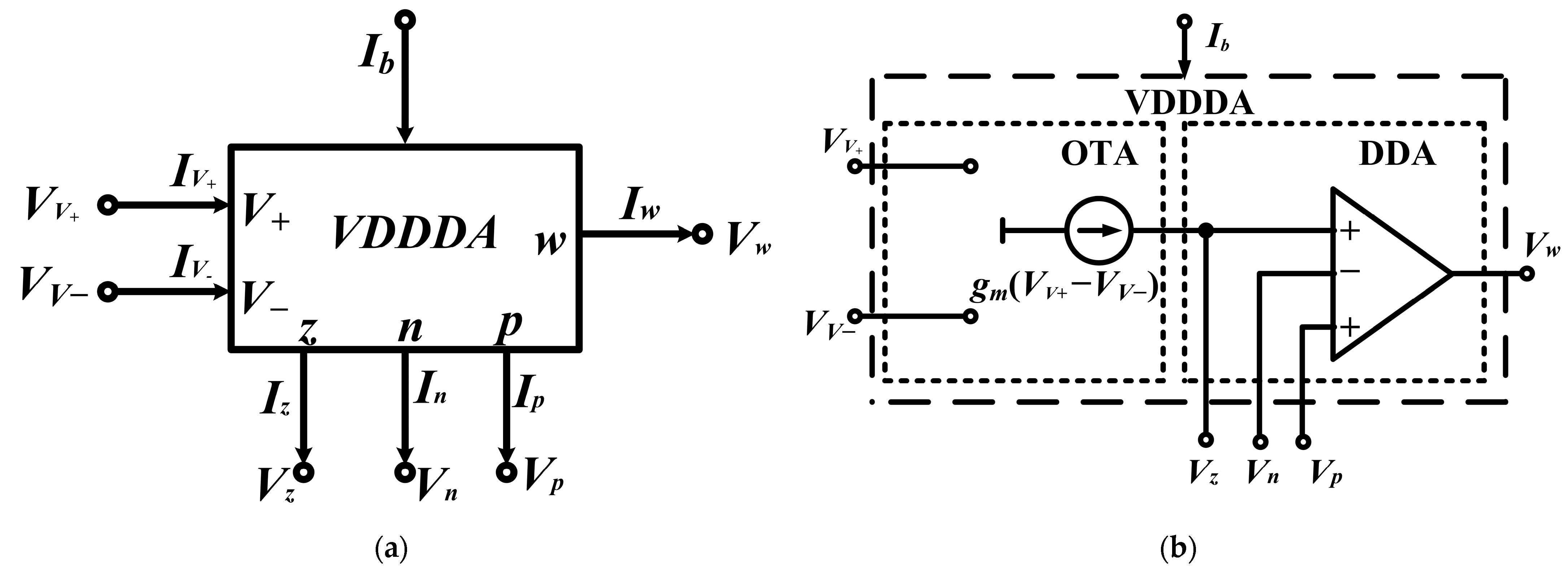
Figure 1. VDDDA: (a) symbol; (b) behavioral model.
Fractalfract 08 00031 g001
Figure 2. CMOS structure of proposed VDDDA.
Fractalfract 08 00031 g002
Figure 3. Layout of BD-VDDDA.
Fractalfract 08 00031 g003
Figure 4. DC analysis: (a) OTA section; (b) DDA section.
Fractalfract 08 00031 g004
Figure 5. AC analysis: (a) OTA section; (b) DDA section.
Fractalfract 08 00031 g005
Figure 6. Output noise of VDDDA.
Fractalfract 08 00031 g006
Figure 7. FBD IFLF [3].
Fractalfract 08 00031 g007
Figure 8. Proposed FO-LPF using VDDDA.
Fractalfract 08 00031 g008
Figure 9. VDDDA model considering parasitic impedances.
Fractalfract 08 00031 g009
Figure 10. Layout of proposed FOF.
Fractalfract 08 00031 g010
Figure 11. LP filter characteristics for different orders: (a) magnitude; (b) phase. (Pre-layout: solid line; post layout: dotted line).
Fractalfract 08 00031 g011
Figure 12. Filter characteristics showing exact curves, pre-layout, and post-layout simulation results: (a) magnitude; (b) phase. (Pre-layout: solid line).
Fractalfract 08 00031 g012
Figure 13. LP filter characteristics at different pole frequencies for order 1.5: (a) magnitude; (b) phase. (Pre-layout: solid line; post layout: dotted line).
Fractalfract 08 00031 g013
Figure 14. Output noise of low-pass FOF.
Fractalfract 08 00031 g014
Figure 15. Linearity plot for low-pass FOF.
Fractalfract 08 00031 g015
Figure 16. Time-domain responses of FO-LPF.
Fractalfract 08 00031 g016
Figure 17. Magnitude characteristics for process variations.
Fractalfract 08 00031 g017
Figure 18. Magnitude characteristics for temperature variations.
Fractalfract 08 00031 g018
Figure 19. Magnitude characteristics for voltage variations.
Fractalfract 08 00031 g019
Figure 20. (a) Monte-Carlo analysis of FO-LPF, (b) Histogram plot for 600 run cycles.
Fractalfract 08 00031 g020
Figure 21. Sensitivity plot of the proposed filter with respect to tracking-error parameters.
Fractalfract 08 00031 g021
Figure 22. (a) The original ECG signal; (b) the noisy ECG signal; (c) the filtered ECG signal.
Fractalfract 08 00031 g022aFractalfract 08 00031 g022b
Table 1. Aspect ratio of transistors of VDDDA.
TransistorW (μm)/L (μm)
M1, M212/0.6
M3–M5, Mb1, Mb2, Mdc1, Mdc210/0.6
M6, M9, M107/0.6
M7, M84/0.6
M11–M144/0.3
M15–M1810/0.3
M1920/0.3
Table 2. Parameter values for different values of orders for f0 = 1 kHz.
Order of Filter1.31.51.71.9
C1 [pF]90909090
C2 [pF]90909090
C3 [pF]30303030
RA [kΩ]21.6710.5
RB [kΩ]4.643.42.8
gm1 [nS]150172190210
gm2 [nS]619650652607
gm3 [nS]643537485475
Ib1 (nA)12.312.512.914.5
Ib2 (nA)727474.165
Ib3 (nA)75534746
Table 3. Theoretical and simulated slope of attenuation for different values of orders for f0 = 1 kHz.
Order of FilterSlope of Attenuation [dB/dec]
TheoreticalSimulated
1.32626.04
1.53030.57
1.73433.64
1.93837.61
Table 4. Parameter values for different values of frequencies with order 1.5.
Pole Frequency500 Hz1 kHz2 kHz
C1 [pF]909090
C2 [pF]909090
C3 [pF]303030
RA [kΩ]1.671.671.67
RB [kΩ]444
gm1 [S]85.8 n172 n343 n
gm2 [S]325 n650 n1.3 μ
gm3 [S]269 n537 n1.07 μ
Ib1 (nA)512.529
Ib2 (nA)2674150
Ib3 (nA)2053145
Table 5. Theoretical and post-layout simulated pole frequency values for order 1.5.
Theoretical Pole FrequencySimulated Pole Frequency
500 Hz502 Hz
1 kHz1.003 kHz
2 kHz2.007 kHz
Table 6. Relative studies of the proposed FO-LPF with fractional filters available in the literature.
[Ref.] (Year)Type (Number) of ABB UsedFunction RealizedNo. of Passive Elements
(R, C)
Grounded/Floating
Elements
Supply VoltageElectronic TunabilityUse of LV-LP
Technique
Total Power Dissipation (W)
[6] (2016)CCII (4), DDCC (1)LPF7, 3GNANoNoNA
[14] (2011)OPAMP (2)LPF10, 3FNANoNoNA
[15] (2018)CFOA (4)LPF9, 3F±10 VNoNoNA
[16] (2016)CFOA (4)LPF10, 3F±10 VNoNoNA
[17] (2018)OTA (3), MOCF (1), ACF (2)LPF0, 3G±1 VYesNoNA
[18] (2017)OTA (3), CF (1), ACA (3)LPF0, 3GNAYesNoNA
[19] (2016)DDCC (5)LPF7, 3G±0.5 VNoYes0.185 m
[20] (2020)CDBA (5)LPF, BPF11, 3F±10 VNoNoNA
[21] (2017)UVC (4)LPF10, 3FNANoNoNA
[32] (2018)MOCF (2), DOCF (1), ACA (5)LPF3, 3FNAYesNoNA
[33] (2017)ACA (5), FD-CF (3)LPF6, 3FNAYesNoNA
[34] (2019)OTA (8), CF (1)LPF, HPF, BPF, BRF0, 3G±0.75 VYesNo8.74 μ
[35] (2021)OTA (6), CF (3), ACA (1)LPF0, 1 *G±1.65 VNoNo72.6 m
[36] (2022)CDBA (4)APF11, 3FNAYesNoNA
[37] (2023)CFTA (5)LPF2, 3G±0.9 VYesNo6.8 m
ProposedVDDDA (3), MOS (6)LPF0, 3G±0.3 VYesYes663 n
* Uses 5 fractional-order capacitors.
Disclaimer/Publisher’s Note: The statements, opinions and data contained in all publications are solely those of the individual author(s) and contributor(s) and not of MDPI and/or the editor(s). MDPI and/or the editor(s) disclaim responsibility for any injury to people or property resulting from any ideas, methods, instructions or products referred to in the content.