Abstract
In this article, a second-order iterated Circular Minkowski fractal antenna (CMFA) tailored for ultra-wideband (UWB) applications is designed and developed. Leveraging the power of Minkowski fractal geometry, this antenna design achieves a high gain across the UWB frequency spectrum. The design utilizes a circular groove on the ground plane and an arc slot on the radiating element for improving the antenna performance. The proposed antenna is fabricated using cost-effective material, an FR-4 substrate. The antenna is simulated and optimized. The fabricated optimized antenna undergoes real-world testing. Measured results reveal an impressive 120.6% impedance bandwidth spanning from 3.37 GHz to 13.6 GHz, with resonant frequencies at 4.43 GHz, 6.07 GHz, and 9.3 GHz. Meanwhile, the simulated results indicate an impedance bandwidth of 118% ranging from 3.17 GHz to 12.44 GHz. Real-world measurements validate the anticipated UWB traits, closely aligning with the simulation data, and confirming efficient impedance matching with a VSWR of less than 2 across the 3.37 GHz to 13.6 GHz frequency range. The radiation pattern analysis demonstrates a robust bidirectional E-plane pattern and a nearly omnidirectional H-plane pattern. This research introduces a highly promising circular Minkowski fractal antenna for UWB applications, offering exceptional bandwidth and resonance characteristics. This antenna design holds excellent potential for multi-functional wireless systems and opens avenues for enhanced UWB communication and sensing capabilities in diverse applications.
1. Introduction
Ultra-wideband (UWB) technology holds great promise as a communication system solution due to its ability to transmit data at high speeds and its excellent resistance to multipath interference. In various fields such as satellite communications, aerospace, radar, biomedical applications, mobile communication for GSM, and remote sensing, the microstrip patch antenna has become widely utilized []. This popularity stems from its advantageous features, including ease of analysis and fabrication; affordability; lightweight nature; ease of feeding; the capacity for dual, triple, and multiple frequency operations; as well as its attractive radiation characteristics [,]. Despite its numerous benefits, the patch antenna does possess limitations, particularly in terms of its narrow bandwidth and poor gain.
The demand for wideband antennas operating at higher frequencies has been steadily increasing due to the requirements of various wireless applications for greater bandwidth. Consequently, researchers have been actively working to develop new and effective methods to enhance the different aspects of microstrip patch antennas, particularly their bandwidth. Radiating elements of printed antennas consist of patches with diverse shapes, such as triangular, rectangular, square, elliptical, and circular [,]. Among these options, circular structures have demonstrated smaller dimensions relative to frequency operations. Circular patch antennas offer the advantage of simplified design and control over radiation patterns compared to rectangular antennas, where patch length and width are utilized for control and design purposes. Furthermore, circular patch antennas are approximately 16% smaller in size compared to rectangular patch antennas operating at the same design frequency.
In recent years, there has been considerable progress in UWB technology and wideband antennas. These advancements have led to the development of novel circular patch antenna designs that address the limitations of conventional narrow-band patch antennas. By adopting circular patch configurations, engineers have been able to overcome the narrow bandwidth issues associated with traditional designs. The smaller size of circular patch antennas not only aids in reducing space requirements but also enhances their compatibility with compact communication devices [].
The circular patch antenna’s advantageous characteristics extend beyond its compactness and simplified design. Circular patches offer wider bandwidths, making them suitable for applications that demand high-speed data transmission []. The enhanced bandwidth capability enables circular patch antennas to support a broader range of frequencies, facilitating seamless connectivity for various wireless communication systems. This versatility is crucial in modern communication environments where multiple wireless devices coexist, operating on different frequency bands.
Moreover, circular patch antennas exhibit favorable radiation properties, including improved directivity and radiation efficiency [,]. The circular geometry allows for the generation of desirable radiation patterns with enhanced gain and reduced side lobes. These features contribute to better signal reception and transmission, ensuring reliable and efficient communication in complex environments.
To optimize the performance of circular patch antennas, researchers employ advanced techniques and materials. The use of innovative substrate materials with high dielectric constants allows for increased miniaturization and improved antenna efficiency. Furthermore, the incorporation of fractal geometries in circular patch designs has shown promising results in further enhancing their bandwidth and radiation properties. In today’s communication landscape, wireless connectivity is essential for devices to support multiple applications with different center frequencies. While using multiple antennas can enable multiband operations, this approach comes with several drawbacks. Firstly, it increases the overall cost and size of the device, making it less practical for certain applications. Also, the system’s complexity increases as multiple antennas require additional components and circuitry to function properly. Moreover, the usage of multiple antennas creates coupling issues, which can adversely affect the performance of the antennas. Coupling leads to interference and reduced efficiency, resulting in degraded signal quality and overall system performance.
To overcome these challenges, several alternative approaches to achieving multiband operations without relying on multiple antennas have been developed; this includes the development of wideband antennas that can cover a broad frequency range while maintaining a compact form factor []. However, a notable issue with this design is the introduction of notch bands in the antenna structure. In an effort to enhance the bandwidth of microstrip patch antennas, these advancements aim to meet the increasing demands of communication systems while simultaneously reducing costs, size, and complexity. This study suggests the utilization of fractal geometry to reduce the size of the radiating patch and enhance the antenna’s gain when operating in the UWB bandwidth.
This research introduces the design and analysis of the second-order iterated circular Minkowski fractal antenna (CMFA) on the design presented in [] tailored for ultra-wideband applications. The proposed CMFA offers several appealing features, including high gain, a small form factor, and the ability to operate across the entire UWB frequency spectrum. The antenna features a microstrip feedline and employs Minkowski fractal geometry to optimize its gain across the UWB frequency spectrum. The design integrates a circular groove on the ground plane along with an arc slot at the periphery of the radiating element. The modified UWB CMFA antenna utilizes a circular patch and a single microstrip feedline, while adopting the cost-effective FR-4 substrate and copper for the radiating component. The design and simulation of this UWB CMFA antenna are carried out using the time-domain solver within the Computer Simulation Technology (CST) Studio Suite 2020 by Dassault Systèmes. To validate the real-world usability of the proposed fractal antenna, it is fabricated and subjected to measurements of S-parameters and radiation characteristics. These measurements are performed using the Rhodes and Schwarz ZVL vector network analyzer (VNA) and a radio frequency (RF) anechoic chamber, respectively.
The remaining sections of the paper are organized as follows: Section 2 presents the design and geometry of the circular Minkowski fractal antenna, and Section 3 presents the characteristics of the antenna. The fabricated measured results and validation of the measured results with simulated results are presented in Section 4, and Section 5 presents the conclusion of the work.
2. Design and Geometry of the Circular Minkowski UWB Antenna
The top view, bottom view, and side view of the proposed antenna are presented in Figure 1a, Figure 1b, and Figure 1c, respectively. The antenna design incorporates a fundamental circular patch configuration with two circular slots located on the left and right edges of the radiating patch, as illustrated in Figure 2a, and features a single feedline. To enhance the antenna’s impedance matching, we introduce a Minkowski square on top of the circular radiating patch as shown in Figure 2b. Additionally, we take a further step to enhance impedance matching by adding an additional iteration of the Minkowski square, as shown in Figure 2c. This modification is aimed at optimizing the antenna’s impedance matching, gain, and efficiency characteristics.
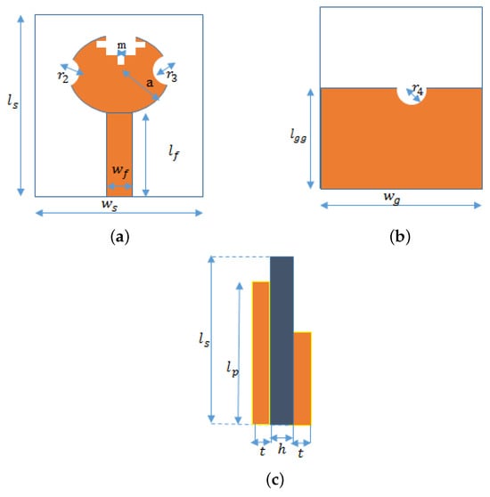
Figure 1.
Geometry of the proposed antenna: (a) top view, (b) bottom view, and (c) side view.
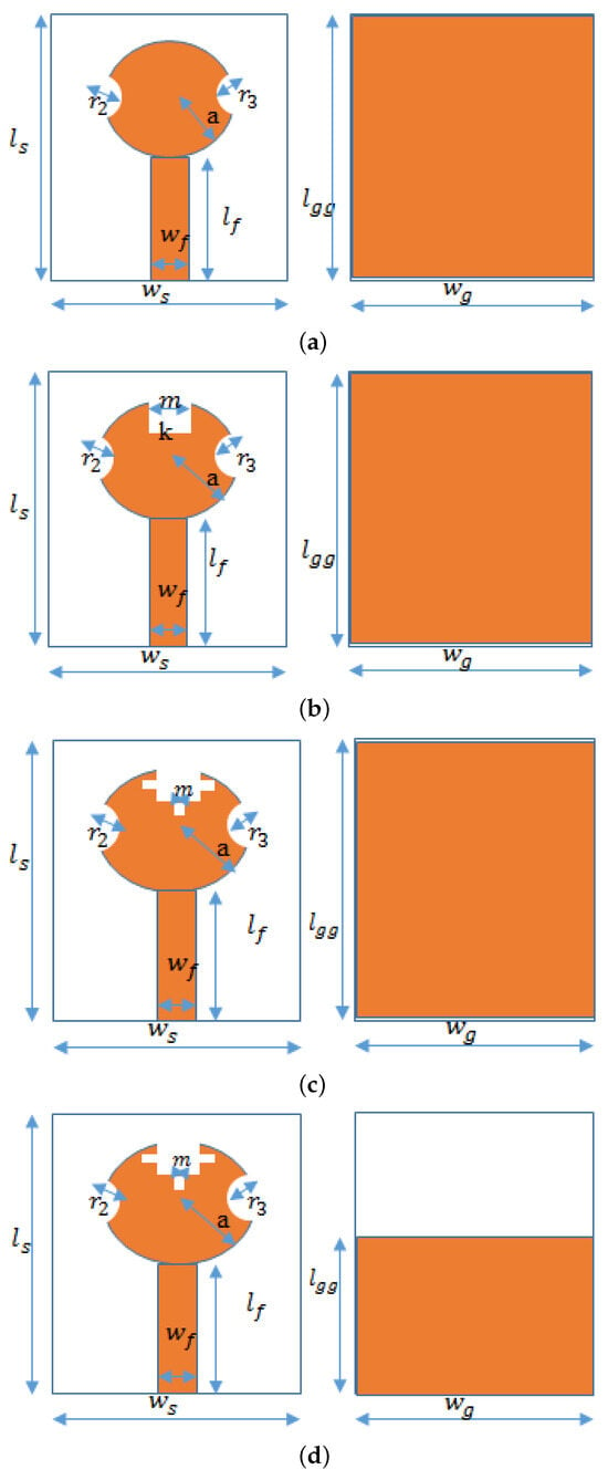
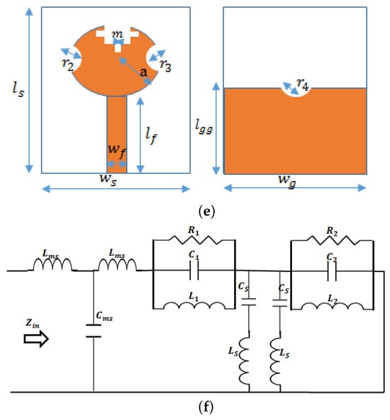
Figure 2.
Design evolution of the circular Minkowski fractal antenna: (a) Ant-1, (b) Ant-2, (c) Ant-3, (d) Ant-4, (e) Ant-5, and (f) the equivalent circuit of the antenna.
To improve the antenna’s bandwidth, we implement a partial ground configuration, as demonstrated in Figure 2d. To further expand the antenna’s bandwidth to cover the entire UWB frequency range, a central groove is introduced on the ground plane, as depicted in Figure 2e. Figure 2e provides a visual representation of the antenna’s ground plane, highlighting the presence of the centrally positioned groove that has been incorporated for this purpose.
The central groove plays a crucial role in improving impedance matching by reducing the capacitive loading on the patch antenna. This occurs because the groove creates an area of low electric field strength at the center of the ground plane, which in turn reduces the amount of current flowing through the patch antenna. As a result, the antenna’s impedance is more closely matched with that of the feedline, leading to enhanced efficiency.
Here are some additional details about the design:
- The antenna is made of FR-4 material with a dielectric constant of 4.4.
- The patch antenna is 17.6 mm in diameter and 1.6 mm thick.
- The feedline has 50 ohms impedance.
- The center groove is 2.46 mm wide and 1.23 mm deep.
- The antenna is designed to operate at a lower cut-off frequency of 3.1 GHz.
The initial antenna design follows the design equations of a planar circular antenna as given below [,,,,,]:
where = lower cut-off frequency, p = feedgap, a = radius of circular patch, and k = constant. The value of k is a constant, which is 1.15, the feed gap p is 0.32, and = 3.1 GHz. Substituting these in the formula gives the radius of the patch as 0.8834 cm. The resonant frequency of the circular patch antenna can be calculated from the equation given below [,,]:
where represents the zeros of the derivative of the Bessel function , which determines the order of the resonant frequency. The dominant mode frequency is calculated by using the following equation [,]:
where is the speed of light and is calculated from Equation (5)
For a circular patch antenna, changing the radius of the patch determines the resonant frequency of the antenna. The characteristic impedance of the microstrip feedline is calculated using the following equations [,]:
The length of the partial ground is given by the relation:
where and p represent the length of the feedline and the feed gap, respectively.
Self-similarity is one of the characteristics of the Minkowski fractal, which indicates that at various sizes, distinct portions of the curve resemble the entire curve. The specific construction technique and the applied parameters determine the Minkowski fractal’s precise fractal dimension. The following equations have been used to estimate the initial size []:
where L is the length of the Minkowski Square, and are the indentation ratios, and are the length and width of the indentation, and n is the iteration number. The equivalent circuit of the proposed CMFA is depicted in Figure 2f. This circuit comprises several elements. Specifically, , , and represent the resistance, inductance, and capacitance of the patch, respectively. Furthermore, and indicate the mutual capacitance and inductance between the patch and the ground plane. The ground plane, on the other hand, is defined by , , and , which signify its resistance, inductance, and capacitance. Lastly, represents the input impedance of the circuit.
3. Antenna Characteristics
The circular Minkowski arc-slotted antenna analysis considers various parameters influencing its performance. The simulations are conducted using the CST microwave studio. The investigation of the proposed antenna reveals that several factors, namely the length of the ground plane, the dimensions of the groove, and the size of the slot on the radiating patch, significantly impact its overall performance. The subsequent subsections provide detailed explanations of the effects of these parameters.
3.1. Effect of the Slots in the Radiating Patch on Impedance Matching
The graphical representation depicted in Figure 3 illustrates how different slots in the radiating patch affect the impedance matching of the radiating patch. Ant-1 exhibits two resonance frequencies at 8.37 GHz and 12.09 GHz, along with corresponding reflection coefficients of −12.09 dB and −18.44 dB. Ant-2 also demonstrates two resonance frequencies at 8.72 GHz and 9.05 GHz, while showing improved impedance matching at these resonant frequencies. Ant-3, the second iteration of the CMFA, reveals three resonant frequencies at 8.68 GHz, 10.02 GHz, and 12.73 GHz, resulting in reflection coefficients of −33.01 dB, −11.56 dB, and −40.04 dB, respectively. It is worth noting that the addition of a fractal structure to the radiating patch enhances both impedance matching and bandwidth.
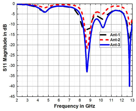
Figure 3.
Effect of the slots in radiating patch.
3.2. Effect of the Length of the Ground Plane on the Bandwidth
The graphical representation in Figure 4 indicates that the antenna with a full ground plane exhibits a narrow bandwidth, while the design goal is to have an antenna that operates across the full UWB frequency range. This antenna shows three resonance frequencies: 8.68 GHz, 10.20 GHz, and 12.73 GHz. The first resonance frequency offers a bandwidth of 0.96 GHz, the second resonant frequency offers a bandwidth of 0.35 GHz, and the latter provides a bandwidth of 0.53 GHz. By reducing the length of the ground plane, the antenna’s bandwidth is increased, and its impedance matching improves, as is evident in Figure 4. Upon reducing the ground plane to 8 mm, the bandwidth increases to 1.32 GHz, and reduction to 7.6 mm increases the bandwidth to 1.75 GHz. A further reduction to 7 mm results in significant bandwidth increment to 5.69 GHz. However, this adjustment moves the lower cut-off frequency further away from the desired design frequency. Subsequently, reducing the ground plane to 6 mm causes the lower cut-off frequency to fall below the design frequency, with a bandwidth of 5 GHz and a reduced reflection coefficient, as observed in Figure 4. At 6.7 mm, we achieve a bandwidth of 5.59 GHz and a lower cut-off frequency of 3.21 GHz, which is remarkably close to the design’s lower cut-off frequency. The trade-off lies in moving the lower cut-off frequency away from or below the desired design frequency. Fine-tuning the ground plane length to 6.7 mm achieves a broader bandwidth while maintaining proximity to the desired cut-off frequency.
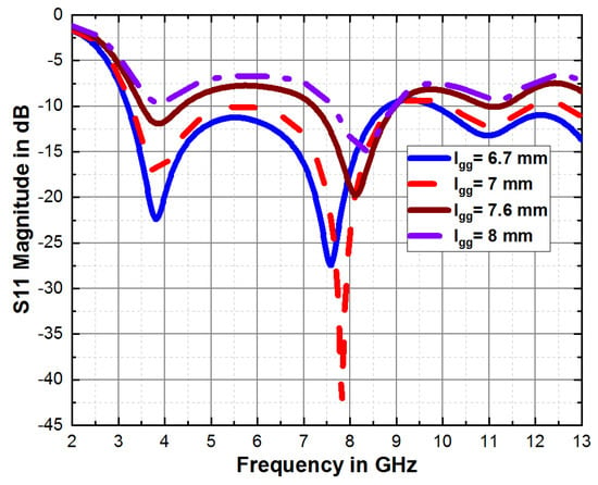
Figure 4.
Effect of the length of ground plane.
3.3. Effect of the Size of Groove
A circular groove is attached to the top-middle of the ground plane to remove the notched band at 8.82 GHz, the dimension of this groove has a significant effect on the bandwidth and reflection coefficient. Simulations were carried out on the groove to obtain a proper radius with good impedance matching and a wide bandwidth. The effect of the radius of the grove is shown in Figure 5. The desired result is obtained with a radius of 2.46 mm. This groove dimension brings down the notch with a good reflection coefficient at the second resonant frequency leading to enhanced overall performance of the antenna.
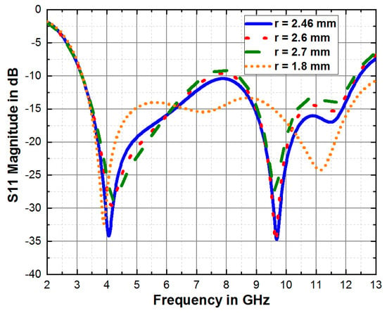
Figure 5.
Effect of the size of the center groove.
The dimensions of this groove play a crucial role in determining the antenna’s bandwidth and reflection coefficient. A radius that is too small has a poor reflection coefficient and a radius that is too big also has an extremely poor reflection coefficient. Therefore, the radius of 2.46 mm was determined as the optimal dimension for achieving the desired outcome in terms of reducing the notch and improving the impedance matching.
3.4. Effect of the Size of the Slot on the Edge of the Radiating Patch
The presence of left and right arc cuts along the middle edge of the radiating patch has a notable impact on the reflection coefficient characteristics of the second resonant frequency. Moreover, these arc cuts introduce a third resonant frequency and enhance the antenna’s bandwidth. Figure 6 demonstrates that a larger arc slot produces a band notch ranging from 7 GHz to 8 GHz with only two resonant frequencies. On the other hand, an exceedingly small, slotted arc results in a poor reflection coefficient despite having two resonant frequencies. The desired outcome is achieved when the radius of the arc is set at 1.6 mm. This radius yields a bandwidth of 10.69 GHz at the resonant frequencies of 4.03 GHz, 9.61 GHz, and 11.48 GHz.
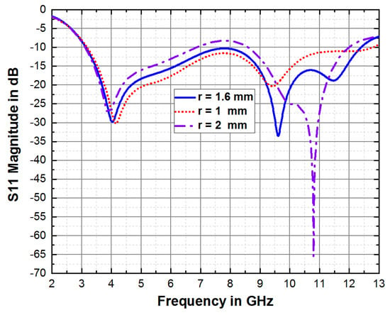
Figure 6.
Simulated reflection coefficient curve for different dimensions of the slotted arc on radiating patch.
3.5. Effect of the Fractal Indentation Ratio
The indentation ratio of the Minkowski fractal plays a crucial role in enhancing both impedance matching and antenna gain. Figure 7 illustrates the results of simulating this phenomenon. It is noticeable that a substantial increase in the indentation ratio shifts the lower cut-off frequency far from the desired frequency. However, this shift is accompanied by improved impedance matching, resulting in the observation of two resonance frequencies at 4.22 GHz and 9.68 GHz. On the other hand, a very small indentation ratio creates a band notch between the C and X bands, covering the range from 7.53 GHz to 8.20 GHz. The trade-off involves deciding between moving the lower cut-off frequency away from the design frequency while maintaining good impedance or moving it to the design cut-off frequency while creating a band notch. Following numerous parametric optimizations, excellent impedance matching was achieved at an indentation ratio of 0.25 mm. This configuration offers significantly improved impedance matching and bandwidth, with a minimum return loss of −34.72 dB at 9.68 GHz and no band notch observed.
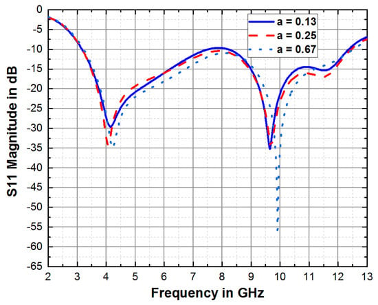
Figure 7.
Simulated reflection coefficient curve for different indentation ratios of the fractal antenna.
4. Results and Discussion
The circular Minkowski fractal antenna with a partial ground plane was constructed using a fire-retardant (FR-4) substrate, which was then measured to confirm its UWB performance. The reflection coefficient (S11) in decibels (dB) and voltage standing wave ratio (VSWR) were measured using the VNA with a frequency range of 9 KHz to 13.6 GHz; connectors were employed for connecting the designed antenna to the VNA. Figure 8 and Figure 9 show the captured S11 and VSWR results, respectively, from the VNA. The top view and bottom view of the CMFA prototype are shown in Figure 10a and Figure 10b, respectively. Furthermore, the proposed antenna radiation pattern is examined within an anechoic chamber, with a horn antenna serving as the receiver and the proposed antenna as a transmitter, as illustrated in Figure 10c. The radiation characteristics measurement in the anechoic chamber is shown in Figure 10c,d. The experimental setup for measuring the reflection coefficient is shown in Figure 10e.
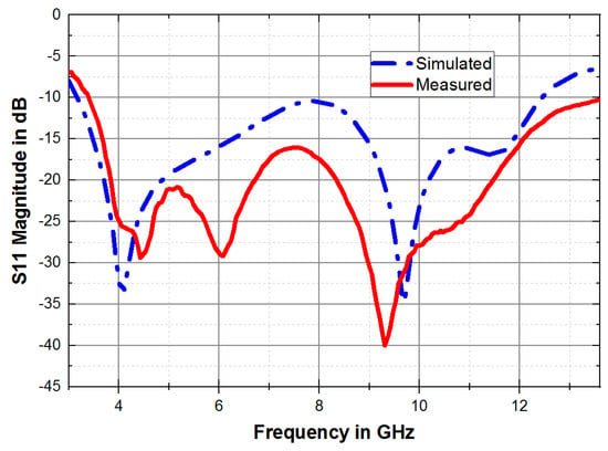
Figure 8.
Reflection coefficient of the circular Minkowski fractal antenna.
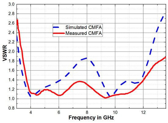
Figure 9.
VSWR of the circular Minkowski fractal antenna.
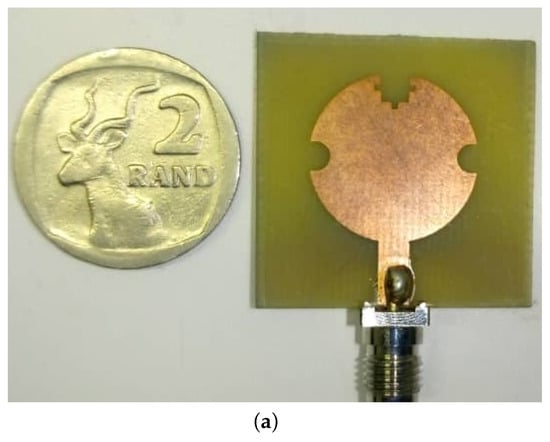
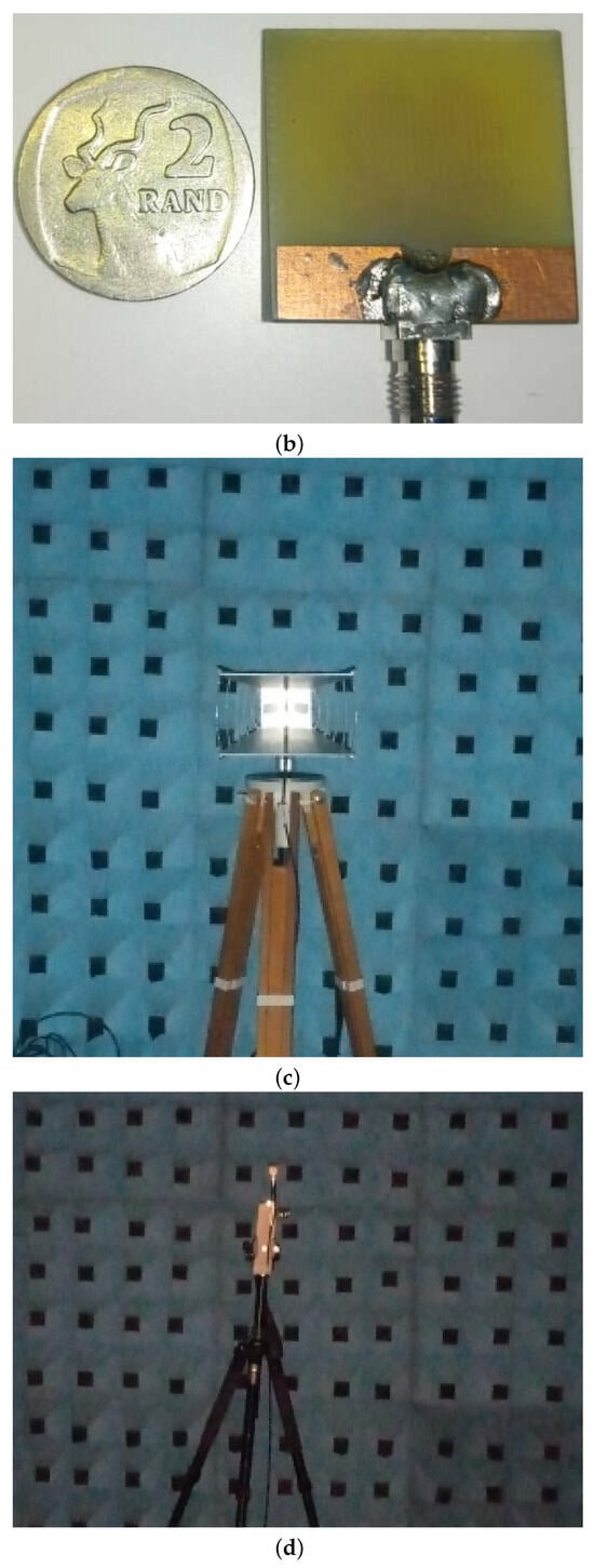
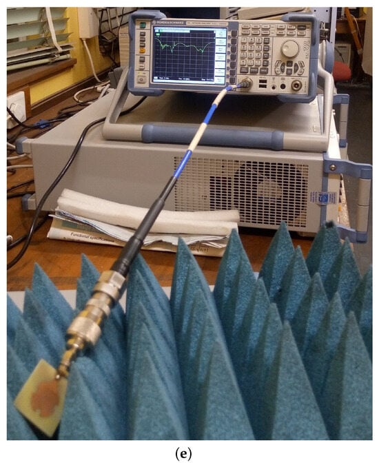
Figure 10.
Fabricated CMFA: (a) front view of the prototype, (b) back view of the prototype, (c) receiver, (d) transmitter, and (e) reflection coefficient measurement setup.
The CMFA’s simulated impedance bandwidth spans from 3.17 GHz to 12.45 GHz, boasting a 118.7% impedance bandwidth. Notably, it achieves a minimum reflection coefficient of −34.71 dB at 9.7 GHz and −34.15 dB at 4.06 GHz. The measured impedance bandwidth of the antenna is observed between 3.37 GHz and 13.6 GHz (with S11 < −10 dB); this presents an impressive 120.6% impedance bandwidth with a minimum reflection coefficient of −40.03 dB. The antenna exhibits three resonant frequencies: 4.43 GHz, 6.07 GHz, and 9.3 GHz, rendering it well-suited for multi-functional wireless applications across the S, C, and X bands. The incorporation of the Minkowski fractal pattern on the antenna leads to enhancements in bandwidth, impedance matching, and gain. Remarkably, a strong correlation is evident between the measured and simulated results. Figure 8 depicts the measured and simulated reflection coefficients of the proposed antenna. The measured S11 closely aligns with the simulated counterpart across the majority of the intended frequency spectrum. The measurements validate the anticipated UWB traits as predicted in the simulation, albeit with a minor deviation observed at the lower edge frequency. Furthermore, the measurements substantiate the pass-band characteristics, as demonstrated in Figure 8. Discrepancies between the measured and simulated outcomes are largely attributed to fabrication and soldering tolerances of the SMA connector, which are aspects that the simulation fails to account for. Additionally, the simulation maintains a constant dielectric loss tangent for the FR-4 substrate, while in reality, this tangent varies with frequency.
Figure 9 illustrates the VSWR for the circular Minkowski fractal antenna. The circular Minkowski fractal antenna demonstrates a VSWR of less than 2 across the frequency range of 3.37 GHz to 13.6 GHz, which is a validation conducted through VNA testing. The antenna’s gain is determined utilizing the comparative gain measurement technique within a 5 m × 3 m × 3 m anechoic chamber and is calculated using the following equations [,]:
where R is the distance between the transmitting and receiving antennas, is the power of the standard gain antenna, is the gain of the standard gain antenna, is the power of the antenna under test, is the gain of the antenna under test, is the power of transmitting antenna, is the gain of transmitting antenna, and is the operating wavelength. Dividing Equation (11) by Equation (12),
Converting to dB scale,
The measurement is taken at the far field region.
where D is the broader dimension of the antenna, and S is the minimum distance between the transmitting antenna and the receiving antenna.
The radiation pattern was simulated, and measurements were carried out within an anechoic chamber. Figure 11a–e depict the simulated and measured radiation patterns at 4.02, 9.07, and 11.48 GHz. In particular, the E-plane radiation patterns, as seen in the measured data, closely align with the simulation results, exhibiting a figure-of-eight shape indicative of a robust bidirectional pattern. Conversely, the H-plane pattern appears to be nearly omnidirectional. Overall, the measured E-plane pattern more closely mirrors the simulated pattern compared to the H-plane pattern. It is worth noting that the measured curves display numerous ripples and distortions, likely stemming from factors such as soldering residue, feed connectors, fabrication, and assembly errors. The simulated and measured parameters of the CMFA are presented in Table 1. It can be seen that there is a noticeable enhancement in the antenna’s fractional bandwidth from the measured result.
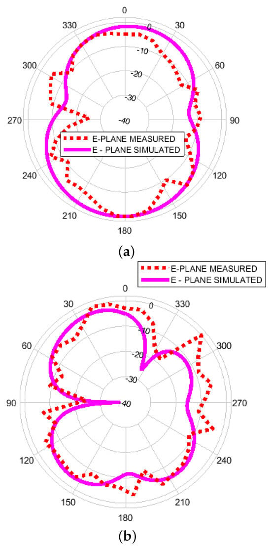
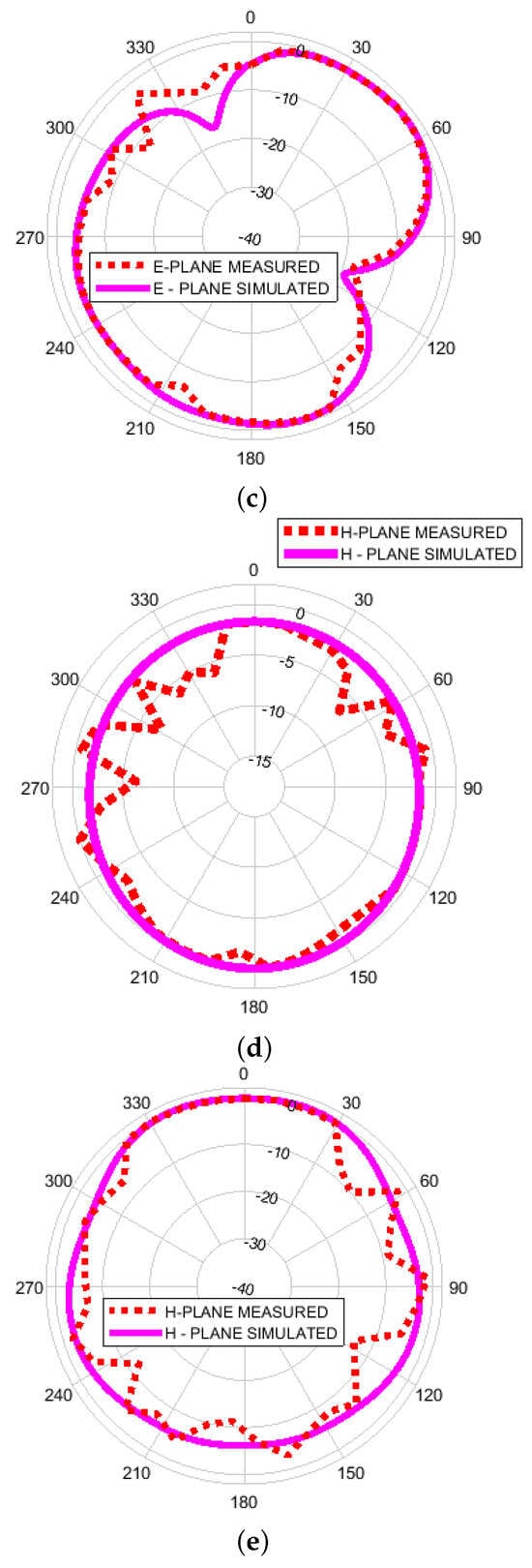
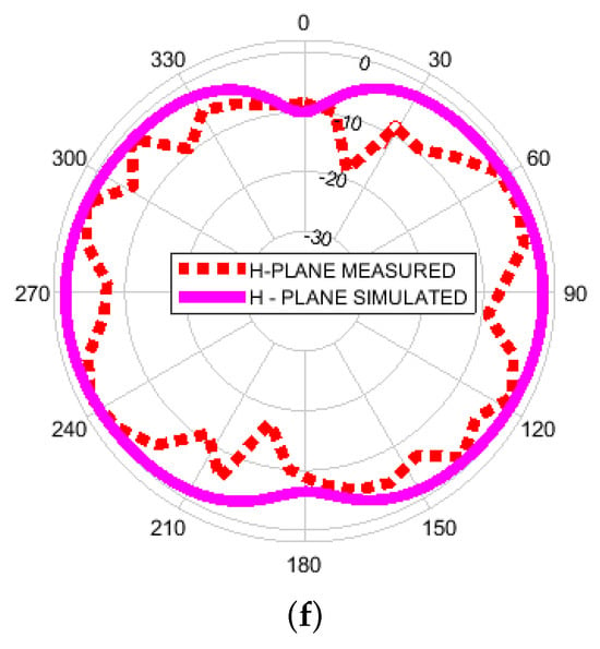
Figure 11.
Simulated and measured normalized radiation patterns of the circular Minkowski fractal antenna: (a) E-Plane (4.02 GHz), (b) E-Plane (9.7 GHz), (c) E-Plane (11.48 GHz), (d) H-Plane (4.02 GHz), (e) H-Plane (9.7 GHz), (f) H-Plane (11.48 GHz).

Table 1.
Summary of the simulated and measured parameters of the CMFA.
Figure 12 shows the surface current distribution on the CMFA; it can be seen that different frequencies show different patterns in the surface current. When the frequency is set to 4.02 GHz, it is more pronounced in the patch’s central arc slot and along the lower edge of the radiating patch. The surface current also becomes more prominent at 9.7 GHz along the radiating patch’s upper corner and bottom edge. Finally, at 11.48 GHz, the surface current significantly increases along the radiating patch’s lower edge and arc-shaped slots, resulting in a variety of behaviors at various frequencies. The interactions between electromagnetic waves and the radiating patch’s shape at the relevant frequencies are thought to be the cause of these events. At 4.02 GHz, the surface current is more noticeable along the bottom edge and the central arc slot of the radiating patch due to the resonance effects created by the geometry of the patch at that frequency. Similarly, at 9.7 GHz, the surface current becomes more prominent along the lower edge and upper corner of the patch due to the specific dimensions and layout of the patch, which resonate with the electromagnetic waves at that frequency. Lastly, at 11.48 GHz, the notable increase in surface current along the lower edge and arc-shaped slots can be attributed to another resonance effect caused by the interaction between the electromagnetic waves and the intricate features of the patch. In essence, the geometry and layout of the radiating patch play a critical role in determining how the surface current distribution responds to different frequencies, resulting in the observed patterns.
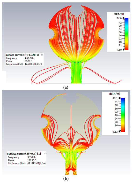
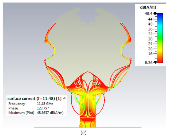
Figure 12.
Surface current distribution on the CMFA at (a) 4.02 GHz, (b) 9.7 GHz, and (c) 11.48 GHz.
The maximum gain, directivity, radiation efficiency, and overall efficiency of the antenna at various frequencies are shown in Table 2. The antenna’s highest gain, 6.25 dB precisely at 9.7 GHz, is noteworthy and indicates improved directionality at this frequency. Additionally, it is clear that as the frequency within the UWB increases, so does the radiation efficiency and overall efficiency of the antenna. The performance of the proposed antenna is compared with other existing work in the literature, as shown in Table 3. It is evident from Table 3 that the proposed CMFA has significantly improved gain and miniaturization with wideband characteristics.

Table 2.
Gain, directivity, radiation efficiency, and total efficiency of CMFA.

Table 3.
Comparison of the designed UWB CMFA with the existing antennas in the literature.
5. Conclusions
A circular Minkowski fractal antenna of the second order custom-designed for UWB applications has been presented in this paper. The antenna employs innovative Minkowski fractal geometry, coupled with modifications to the ground plane and microstrip feedline, resulting in substantial performance improvements across the UWB frequency spectrum. The viability of this fractal antenna is established through a comprehensive process encompassing design, simulation, fabrication, and measurement. In simulations, the antenna exhibits an impedance bandwidth of 118%, spanning from 3.17 GHz to 12.44 GHz. In practical measurements, it demonstrates an impressive impedance bandwidth of 120.6%, ranging from 3.37 GHz to 13.6 GHz with a minimum reflection coefficient of −40.03 dB. These characteristics make it a promising candidate for multi-functional wireless applications in the S, C, and X bands. Comparing the simulated and measured results reveals a strong correlation and validation of the antenna’s performance through VNA, indicating a VSWR of less than 2 across the frequency range, which further underscores its suitability for practical applications. Additionally, an analysis of the surface current distribution unveils the intricate relationship between the antenna’s geometry and its response to different frequencies. These insights shed light on radiation patterns and provide valuable data for future optimizations. In conclusion, the antenna parameters affirm that the designed and developed circular Minkowski fractal antenna has proven its worth as a promising choice for UWB applications.
Author Contributions
Conceptualization, E.J., P.K. and T.A.; methodology, E.J., P.K. and T.A.; software, E.J.; validation, E.J., P.K. and T.A.; Writing—E.J. and P.K.; Writing—review and editing, E.J., P.K. and T.A.; supervision, P.K. and T.A. All authors have read and agreed to the published version of the manuscript.
Funding
This research received no external funding.
Data Availability Statement
Not applicable.
Conflicts of Interest
The authors declare no conflict of interest.
References
- Kumar, O.P.; Kumar, P.; Ali, T.; Kumar, P.; Vincent, S. Ultrawideband Antennas: Growth and Evolution. Micromachines 2022, 13, 60. [Google Scholar] [CrossRef] [PubMed]
- Zhang, C.; Zhao, Z.; Xiao, P.; Yu, J.; Liu, Z.; Li, G. A miniaturized microstrip antenna with tunable double band-notched characteristics for UWB applications. Sci. Rep. 2022, 12, 19703. [Google Scholar] [CrossRef]
- Ngobese, B.W.; Kumar, P. A High Gain Microstrip Patch Array for 5 GHz WLAN Applications. Adv. Electromagn. 2018, 7, 93–98. [Google Scholar] [CrossRef]
- Liang, J.; Chiau, C.C.; Chen, X.; Parini, C.G. Study of a printed circular disc monopole antenna for UWB systems. IEEE Trans. Antennas Propag. 2005, 53, 3500–3504. [Google Scholar] [CrossRef]
- Awad, N.M.; Abdelazeez, M.K.; Al-Sharif, A.; Awad, N.M.; Abdelazeez, M.K.; Al-Sharif, A. Enhanced UWB Printed Monopole Antenna Based on Ground Plane Modifications. Jordanian J. Comput. Inf. Technol. 2018, 1, 1. [Google Scholar]
- Kumar, O.P.; Kumar, P.; Ali, T. A Compact Dual-Band Notched UWB Antenna for Wireless Applications. Micromachines 2022, 13, 12. [Google Scholar] [CrossRef] [PubMed]
- Pal, A.; Mishra, P.K.; Singh, T.; Tripathi, V.S. A Compact Ultrawideband Planar Patch Antenna for UWB/X/Ku Band Applications. In Proceedings of the 2022 IEEE Microwaves, Antennas, and Propagation Conference, MAPCON 2022, Bangalore, India, 12–16 December 2022; pp. 1063–1067. [Google Scholar] [CrossRef]
- Zayani, Z.; Jam, S. Compact Dual Notched Band UWB Antenna Using DGS and Slots with its Equivalent Circuit. Iran. J. Sci. Technol.-Trans. Electr. Eng. 2023, 47, 327–336. [Google Scholar] [CrossRef]
- Joseph, E.; Kumar, P.; Afullo, T. Design and performance analysis of a miniaturized circular arc slotted patch antenna for ultrawideband applications. In Proceedings of the 2023 International Conference on Electrical, Computer and Energy Technologies (ICECET), Cape Town, South Africa, 16–17 November 2023. [Google Scholar]
- Niture, D.V.; Mahajan, S.P. A Compact Reconfigurable Antenna for UWB and Cognitive Radio Applications. Wirel. Pers. Commun. 2022, 125, 3661–3679. [Google Scholar] [CrossRef]
- Anveshkumar, N.; Gandhi, A.S. Design and performance analysis of a modified circular planar monopole UWB antenna. In Proceedings of the 2017 8th International Conference on Computing, Communication and Networking Technologies (ICCCNT), Delhi, India, 3–5 July 2017; pp. 1–5. [Google Scholar] [CrossRef]
- Gayatri, T.; Srinivasu, G.; Chaitanya, D.M.K.; Sharma, V.K. A compact Luna shaped high gain UWB antenna in 3.1 GHz to 10.6 GHz using FR4 material substrate. Mater. Today Proc. 2021, 49, 359–365. [Google Scholar] [CrossRef]
- Srinivasu, G.; Gayatri, T.; Meshram, M.K.; Sharma, V.K. Design Analysis of an Ultra-Wideband Antenna for RF Energy Harvesting in 1.71–12GHz. In Proceedings of the 2020 11th International Conference on Computing, Communication and Networking Technologies (ICCCNT), Kharagpur, India, 1–3 July 2020; pp. 1–6. [Google Scholar] [CrossRef]
- Gayatri, T.; Srinivasu, G.; Chaitanya, D.M.K.; Sharma, V.K. Design Analysis of a Luna Shaped UWB Antenna for Spectrum Sensing in 3.1–10.6 GHz. In Proceedings of the 2020 IEEE 17th India Council International Conference (INDICON), IEEE, New Delhi, India, 10–13 December 2020; pp. 1–5. [Google Scholar] [CrossRef]
- Sandhu, M.Y.; Afridi, S.; Anjum, M.R.; Chowdhry, B.S.; Khand, Z.H. Ultra Wide Band (UWB) Horseshoe Antenna for Future Cognitive Radio Applications. Wirel. Pers. Commun. 2022, 122, 1087–1099. [Google Scholar] [CrossRef]
- Balanis, C.A. Antenna Theory: Analysis and Design, 4th ed.; John Wiley & Sons: Hoboken, NJ, USA, 2016. [Google Scholar]
- Pozar, D. Microwave Engineering; John Wiley & Sons: Hoboken, NJ, USA, 2011; Volume 2, p. 2. [Google Scholar]
- Kumar, G.; Ray, K.P. Broadband Microstrip Antennas; Artech House: Norwood, MA, USA, 2003. [Google Scholar]
- Garg, R.; Bhartia, P.; Bahl, I.; Ittipiboon, A. Microstrip Antenna Design Handbook; Artech House: Norwood, MA, USA, 2001. [Google Scholar]
- Vallappil, A.K.; Khawaja, B.A.; Rahim, M.K.A.; Uzair, M.; Jamil, M.; Awais, Q. Minkowski–Sierpinski Fractal Structure-Inspired 2 × 2 Antenna Array for Use in Next-Generation Wireless Systems. Fractal Fract. 2023, 7, 158. [Google Scholar] [CrossRef]
- Mayhew-Ridgers, G.; Jaarsveld, P.A.V.; Odendaal, J.W.; Joubert, J. Accurate gain measurements for large antennasusing modified gain-transfer method. IEEE Antennas Wirel. Propag. Lett. 2014, 13, 369–371. [Google Scholar] [CrossRef]
- Ali, T.; Biradar, R.C. A Miniaturized Volkswagen Logo UWB Antenna with Slotted Ground Structure and Metamaterial for GPS, WiMAX and WLAN Applications. Prog. Electromagn. Res. C 2017, 72, 29–41. [Google Scholar] [CrossRef]
- Peram, A.; Reddy, A.S.R.; Prasad, M.N.G. Miniaturized Single Layer Ultra Wide Band (UWB) Patch Antenna Using a Partial Ground Plane. Wirel. Pers. Commun. 2019, 106, 1275–1291. [Google Scholar] [CrossRef]
- Lv, Y.; Zhang, J.; Hou, H. A Novel Triple Band-Notched UWB Printed Monopole Antenna. Prog. Electromagn. Res. M 2019, 81, 85–95. [Google Scholar] [CrossRef]
- Kapoor, A.; Mishra, R.; Kumar, P. Wideband miniaturized patch radiator for Sub-6 GHz 5G devices. Heliyon 2021, 7, e07931. [Google Scholar] [CrossRef] [PubMed]
- Meena, M.L.; Gupta, A. Design Analysis of a Semi-Circular Floral Shaped Directional UWB Antenna Integrated with Wireless Multiband Applications. Prog. Electromagn. Res. C 2019, 90, 155–167. [Google Scholar] [CrossRef]
- Chandu, D.S.; Karthikeyan, S.S. A novel broadband dual circularly polarized microstrip-fed monopole antenna. IEEE Trans. Antennas Propag. 2017, 65, 1410–1415. [Google Scholar] [CrossRef]
- Wang, L.; Yu, J.; Xie, T.; Bi, K. A Novel Multiband Fractal Antenna for Wireless Application. Int. J. Antennas Propag. 2021, 2021, 9926753. [Google Scholar] [CrossRef]
- Khan, M.A.; Rafique, U.; Savci, H.Ş.; Nordin, A.N.; Kiani, S.H.; Abbas, S.M. Ultra-Wideband Pentagonal Fractal Antenna with Stable Radiation Characteristics for Microwave Imaging Applications. Electronics 2022, 11, 2061. [Google Scholar] [CrossRef]
- Subhash, B.K.; Kumar, P.; Pathan, S.; Ali, T.; Biradar, R.C. A Sequence of Circular Slotted Nonagon Shape Extended Ultrawideband Antenna for Smart Electronic Systems using Characteristic Mode Analysis. In Proceedings of the 2023 International Telecommunications Conference (ITC-Egypt), Alexandria, Egypt, 18–20 July 2023; pp. 12–16. [Google Scholar] [CrossRef]
Disclaimer/Publisher’s Note: The statements, opinions and data contained in all publications are solely those of the individual author(s) and contributor(s) and not of MDPI and/or the editor(s). MDPI and/or the editor(s) disclaim responsibility for any injury to people or property resulting from any ideas, methods, instructions or products referred to in the content. |
© 2023 by the authors. Licensee MDPI, Basel, Switzerland. This article is an open access article distributed under the terms and conditions of the Creative Commons Attribution (CC BY) license (https://creativecommons.org/licenses/by/4.0/).