Next Article in Journal
Advances and Perspectives in Alkali–Silica Reaction (ASR) Testing: A Critical Review of Reactivity and Mitigation Assessments
Previous Article in Journal
Bayesian Optimized of CNN-M-LSTM for Thermal Comfort Prediction and Load Forecasting in Commercial Buildings
 
 
Due to scheduled maintenance work on our database systems, there may be short service disruptions on this website between 10:00 and 11:00 CEST on June 14th.
Article

EMM Project—LD GRIDS: Design of a Charged Dust Analyser for Moon Exploration

by
Diego Scaccabarozzi
1,*,
Abdelrahman Mohamed Ragab M. Ahmed
1,
Andrea Appiani
1,
Bortolino Saggin
2,
Carmen Porto
3 and
Francesca Esposito
3
1
Department of Mechanical Engineering, Politecnico di Milano, 20156 Milan, Italy
2
CISAS—Industrial Engineering Department, Università degli Studi di Padova, 35131 Padova, Italy
3
INAF OACN—Capodimonte Astronomical Observatory, Istituto Nazionale di AstroFisica, 80131 Napoli, Italy
*
Author to whom correspondence should be addressed.
Designs 2025, 9(3), 70; https://doi.org/10.3390/designs9030070
Submission received: 29 April 2025 / Revised: 5 June 2025 / Accepted: 6 June 2025 / Published: 10 June 2025

Abstract

:
This work presents a comparative design of the sensing elements for the Lunar Dust GRID System (LD GRIDS), a dust analyser conceived to measure charged particles on future lunar missions. LD GRIDS replaces traditional electrodes with continuous conductive grids, i.e., the sensing elements of the instrument, which are able to collect induced charge when charged particles pass through them. The investigation focuses on evaluating the influence of various grid geometrical parameters (size, thickness, and patterns) on the sensor’s performance, either from an electrical or a mechanical perspective. All simulations were carried out using off-the-shelf numerical modelling software, where electrostatic simulation (i.e., induction performance), modal analysis, and quasi-static structural responses under a high acceleration quasi-static load were examined. The results indicate that while grids with round patterns tend to produce a higher induced charge, they also experience higher localised stresses compared to square pattern ones. Moreover, grid size does not significantly affect the instrument sensitivity, whereas increasing the grid thickness significantly reduces peak stresses, with only minor effects on electrostatic performance. Overall, the findings provided valuable insights for optimising the LD GRIDS design, aimed at balancing either electrostatic sensitivity or mechanical resistance, facing the harsh lunar environment.

1. Introduction

Space instrumentation involves the development of customised instruments, engineered to endure extreme outer space conditions, including intense radiation, vacuum environments, and significant thermal variations, while adhering to stringent mass and power constraints. High-precision measurement requirements for many missions necessitate robust and miniaturised designs to ensure operational success. These instruments (spanning imaging systems, spectrometers, magnetometers, and particulate analysers) demand reliability due to the impracticality of in-flight repairs and the high costs of mission failure. Consequently, instrument development generally prioritises redundancy, exhaustive terrestrial testing, and advanced computational modelling to mitigate risks posed by the space environment. Nowadays, space programs aiming at lunar exploration have identified dust mitigation as a mission-critical priority [1,2]. A complication arises from the Moon’s lack of an atmospheric electrical ground, which enables unstable charge accumulation on equipment, exacerbating dust adherence. Indeed, electrostatically charged dust particles can adhere to equipment, degrade performance, and pose hazards to both instrumentation and crew. Lunar dust, with its fine granulometry, abrasive properties, and electrostatic adhesion, presents a critical challenge to mission longevity. Its capacity to degrade mechanical systems, obstruct instrumentation, and infiltrate habitats underscores the urgency of understanding its electrostatic and dynamic behaviour.
Under this perspective, the Dust Trajectory Sensors (DTSs) are gaining attention from the scientific community due to their capability to quantify charged particle flux by measuring the induced charge as dust passes near a collection electrode. Traditional DTSs rely on discrete wire electrodes, connected to a single Charge-Sensitive Amplifier (CSA). Early prototypes utilised 64 electrodes per unit [3,4], while later iterations expanded to 76 electrodes without increasing the volume [5,6].
Recent designs addressed the limitations of bulky, power-intensive systems, enhancing feasibility for extended lunar deployments. The Cassini Cosmic Dust Analyzer (CDA) first provided the usage of grids as sensing elements in space-designed analysers. The instrument was developed with an overall mass of about 16.4 kg and a peak operating power of about 18.38 W (including articulation). The instrument utilises two pairs of grids to measure and detect the charge and the two components of velocity of dust particles [7,8], measuring up to an electric charge of 10−15 C and providing mass sensitivity 106 times greater than previously developed charge detectors. Another example of space-designed DTS can be found in [9], where the authors described the Lunar Dust Experiment (LDEX) on NASA’s LADEE orbiter, which uses a single gold-coated tungsten mesh (0.5 mm pitch) enclosed within a Faraday-cup structure. The instrument was developed with a mass of approximately 3.6 kg, a 15 × 15 × 20 cm size, and with 3.8 W power in operation and 6.11 W as the peak power. The proposed design mitigates solar-wind charging and ultraviolet effects while maximising sensitivity to micrometre-scale ejecta. LDEX’s electrode grid, supported by a deployable cover and precision-machined frame, exemplifies the trade-offs between open area (for charge collection) and mechanical protection in harsh lunar orbit environments.
The JAXA DESTINY mission employs a DTS based on four charge-sensing grid electrodes for dust particle trajectory measurement [10]. It operates based on the impact ionisation mass spectrometer principle and will study micro-debris in space between low Earth orbit (LEO) and geostationary orbit (GEO).
Indeed, in the framework of the future lunar mission, LD GRIDS aim to further reduce the complexity and mass budget of the developed instrument, through integrating the simplicity of the grid-based detector with lightweight geometries and optimised electrode/grids configurations. Thus, the work investigates the possibility of replacing the conventional electrode array with a continuous meshed grid that maximises the sensing area while improving mechanical robustness and charge accumulation sensitivity. Additionally, by reducing the number of sensing electrodes and, consequently, the used CSAs, the sensor’s mass and power consumption would be reduced, with additional benefits on the instrument’s complexity and reliability. A preliminary study has already investigated the mechanical feasibility of a novel grid-based system [11], showing the potential applicability of such a sensing system to a harsh mechanical environment, like the one expected in typical space applications. However, no parametric study has been conducted on the structural design considering the impact of the shape of the grids and geometry on the structural behaviour. Moreover, evaluating how the mechanical design affects induction performance on the sensing elements of the instrument would allow for instrument optimisation, balancing the needs of mechanical robustness and sensing performance.
Thus, the current study details the sensing element (grid) of the LD GRIDS by conducting a comprehensive analysis that shows the effect of different parameters on the grid element performance. A combined computational approach was employed, as follows: mechanical behaviour was assessed via quasi-static and modal analyses to establish stress limits, deformation, and natural frequencies; the electrostatic induction performance was simulated as well, by tracking the accumulated charge on the grounded grid from a model simulating the interaction between the grid and a point-charge particle moving along a normal trajectory.

2. Materials and Methods

Different geometries of the sensing element were investigated to determine the effect of parameters, such as the internal pattern, the size, and the thickness of the grid, on the electrostatic performance. Two patterns of the grids’ holes were compared (i.e., square and round), as well as two sizes (50 mm × 50 mm and 100 mm × 100 mm) and four thicknesses (from 0.1 mm to 0.35 mm). The latter range was selected based on the expected manufacturing process for the grid, i.e., sheet metal stamping. All designs were modelled in COMSOL Multiphysics® version 6.3, using aluminium material (Al6061) properties (density = 2.7 g/cm3; Young’s modulus = 68.9 GPa; Poisson’s ratio = 0.33, Tensile Yield Strength 276 MPa), and were used both for structural and electrostatic simulation.

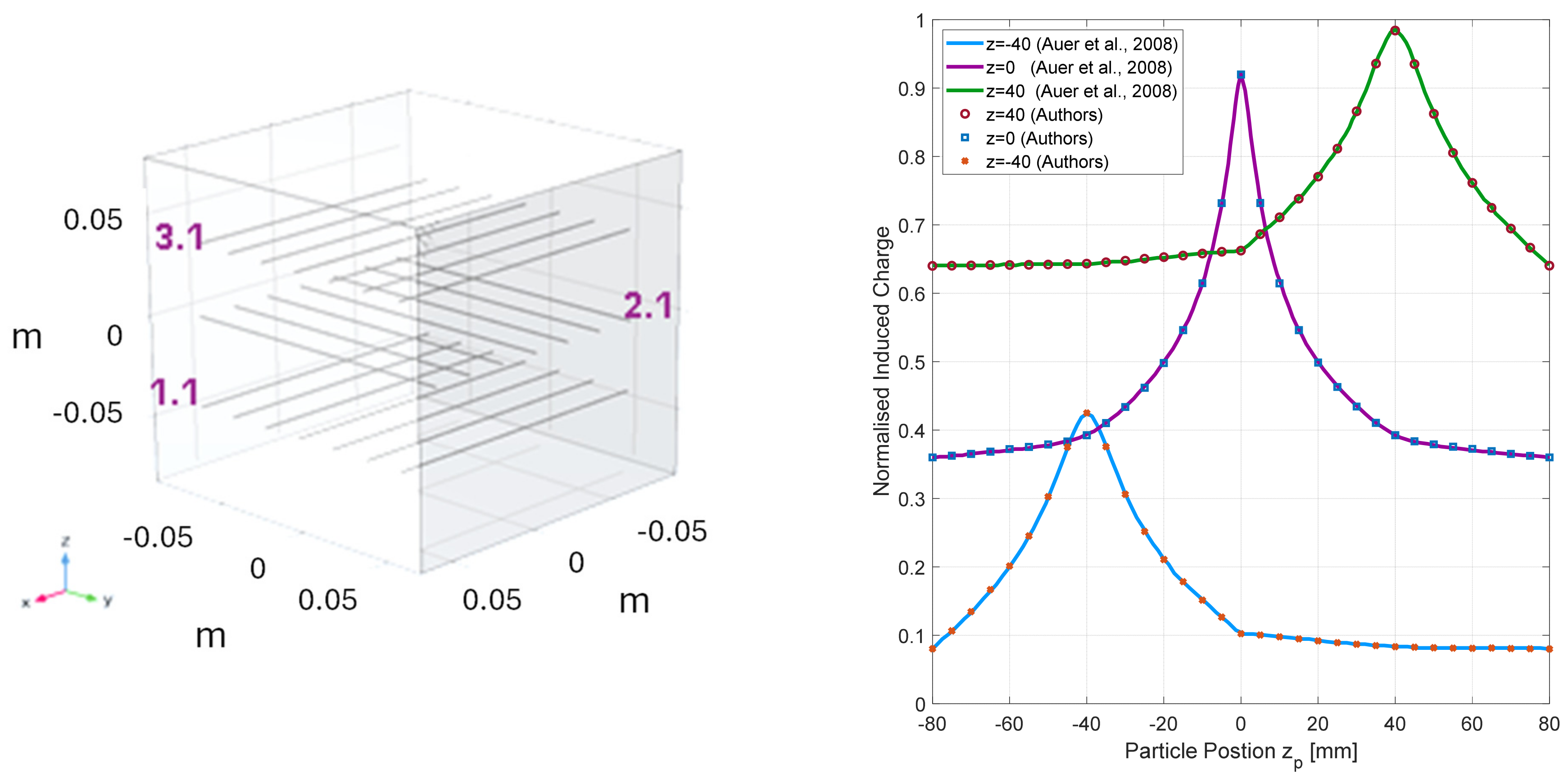
2.1. Electrostatic Modelling Validation

The validation of the implemented methodology was deemed necessary to verify that the numerical simulation accurately reproduces the key features of a Dust Trajectory Sensor (DTS), as established in the previous literature. The previous work of Auer was taken as a reference for the validation [3]. The simulation domain was configured as a 160 mm cube acting as a Faraday cage, within which three equally spaced wire planes were employed. Each wire was modelled as a cylinder with a length of 140 mm, a diameter of 0.4 mm, and spaced 20 mm apart in-plane, while the dust particle was represented by a sphere with a 0.1 mm diameter. The setup adopted a boundary condition with the particle set at +1 V and all other surfaces grounded at 0 V. To emulate conductive behaviour, a large relative permittivity value (1010) was used. This modelling followed the methodology described in the reference literature [3] and was based on the electrostatic physics interface module of the software.
The simulation was coupled with another software (MATLAB 2024b) to automatically generate a set of discrete trajectory points, providing 33 points used in the normal trajectory (from (2, 6, −80) to (2, 6, 80) mm) and 40 points in the oblique trajectory (from (−66, −47, −80) to (78, 53, 80) mm). At each of these points, the induced charge on the surface of each of the 21 wires was calculated through integration of the surface charge density. Normal and oblique trajectories were simulated according to what the authors in [3] carried out. In Figure 1, the modelled case study and the normalised induced charges (computed as the ratio between the induced charge and the particle’s charge) on the simulated planes are compared to the results reported in the reference.
In the first case study (normal trajectory), the model reproduced the largest induced charges, with values of 0.358 and 0.172, closely matching the benchmark values of 0.347 and 0.168—a discrepancy of only 3.1% and 2.4%, respectively. A similar level of accuracy was observed in the oblique trajectory case, with overall differences, for both cases, in the normalised induced charge remaining below 3.5%. These minimal discrepancies were mostly caused by mesh discretisation and the selected number of trajectory points, but the achieved level of accuracy was considered satisfactory for the intended study.
Overall, the results confirmed that the implemented modelling workflow reliably captures the electrostatic effects governing the induced charges on wire arrays. This strong consistency with benchmark data validates the simulation methodology, allowing for its application in the detailed design of LD GRIDS.

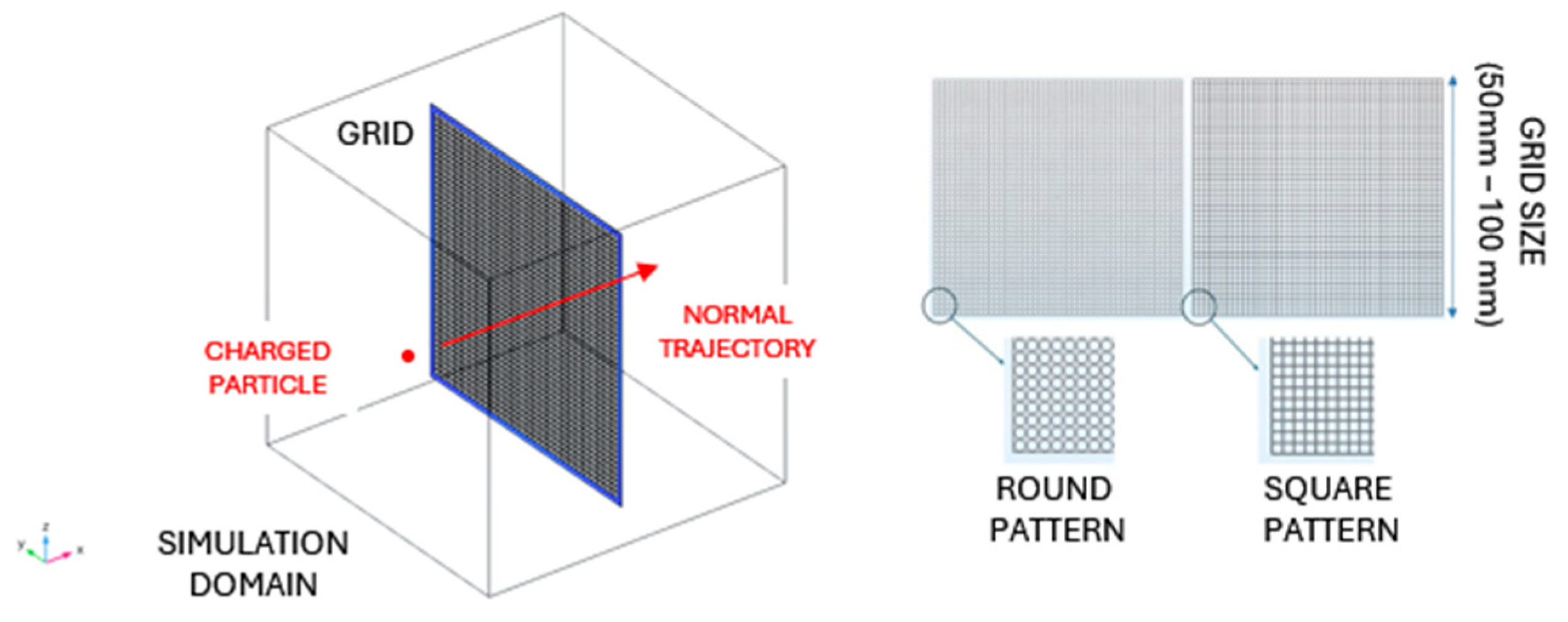
2.2. FE Models Description and Numerical Analyses

Different finite element (FE) models have been developed to investigate the electrostatic and mechanical performance of the proposed design. FE analyses are well-established methods that assess the mechanical and electrical behaviour in different engineering fields, spanning from aerospace to medical research areas [12,13,14,15]. In the following section, model settings used in the study are described and summarised.

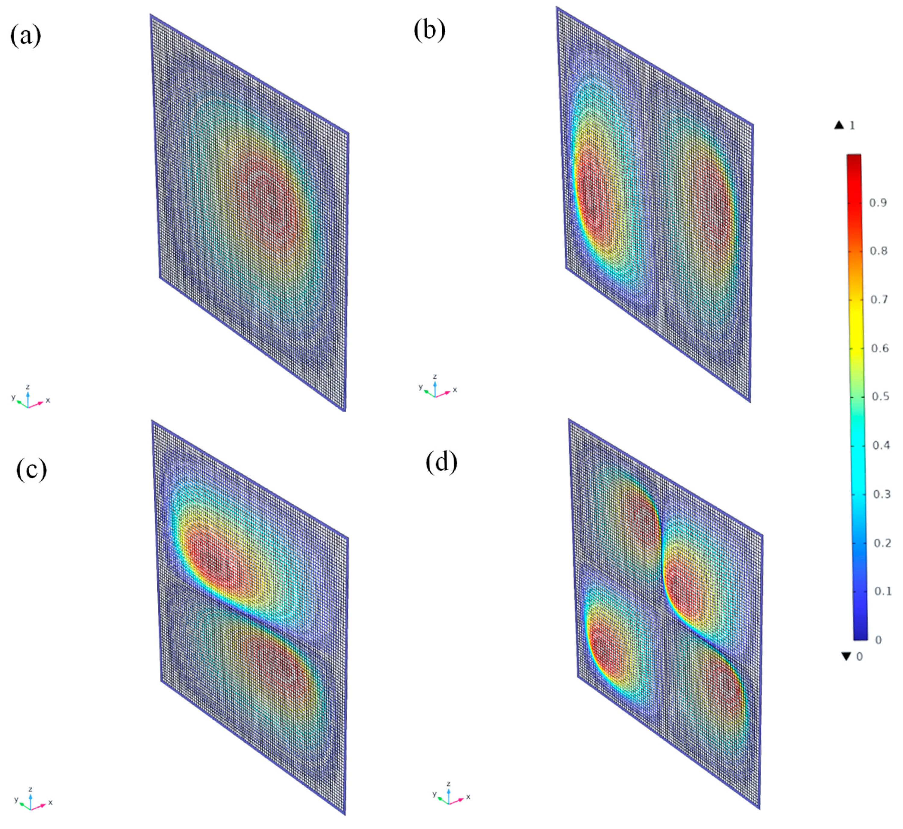
2.2.1. Electrostatic Performance

Electrostatic induction simulations were performed in COMSOL Multiphysics, with each mesh held at ground potential (0 V) and subjected to a charged sphere (50 µm in diameter) of 0.2 fC, traversing perpendicularly at a parameterised distance. Furthermore, two patterns were studied, one with a square geometry (1 mm side) and the second one with a circular shape (1 mm diameter), as shown in Figure 2. The model comprised tetrahedral elements for the simulation domain, the charged sphere, and the grids, i.e., 2,005,403 and 2,299,612 for the square and round patterns, respectively. The parameterised normal distance allows the sphere to change its location along the x-axis, from x p = 20 mm to   x p = 20 mm with a step of 4 mm (total 11 points), while knowing that the grid is centred at x p = 0 mm. The developed model comprised tetrahedral elements ranging from a minimum of 1,096,874 to a maximum of 61,900,723 elements, depending on the modelled geometry.

2.2.2. Modal Analysis

A 3D grid model was developed to conduct the modal analysis. The solid mechanics physics interface was used to compute the eigenfrequencies of the grid. The grid was constrained as shown in Figure 3, i.e., by locking the displacements of the elements at the border in all three directions. The first five natural frequencies and corresponding modal shapes for the four configurations were assessed to evaluate the effect of the grid’s geometry on dynamic stiffness.
For the modal analysis, dynamic behaviour should provide a first natural frequency above 150 Hz to effectively avoid the input given by the sweep sine excitation at launcher take-off [16,17]. The model comprised tetrahedral elements ranging from a minimum of 184,033 to a maximum of 1,163,923 elements.

2.2.3. Quasi-Static Analysis

Quasi-static simulations applied a 100 g (g is meant to be the Earth’s gravity) quasi-static acceleration along the normal direction of the grid, constrained with clamped edges. The latter loading condition is the worst-case scenario, given that the load causes the bending deformability of the grid. Computation of the Von Mises stress distribution on the grid aimed to ensure the grid’s mechanical resistance, assuring the instrument’s functionality in the harsh mechanical environment. A positive assessment is obtained if the maximum Von Mises stress is lower than the admissible one for the used material. The ECSS-E-ST-32-10C standard rules the evaluation of the margin of safety against the limit condition as
M o S = d e s i g n   a l l o w a b l e   s t r e s s d e s i g n   m a x i m u m   s t r e s s × F o S 1
where the Factor of Safety (FoS) is set to 1.25, and the design-allowable stress is given by the material’s admissible stress. The assessment can be considered satisfactory when the MoS is larger than zero. The round and square patterns in both sizes are simulated while applying the same constraints and mesh settings described in the modal analyses.

3. Results and Discussion

3.1. Pattern Influence

In the following section, the comparison between the holes’ patterns on the electrostatic and mechanical performance is provided. Performance was assessed by modifying either the pattern or the geometry. In all of the performed simulations, the grid thickness was set to 0.1 mm.

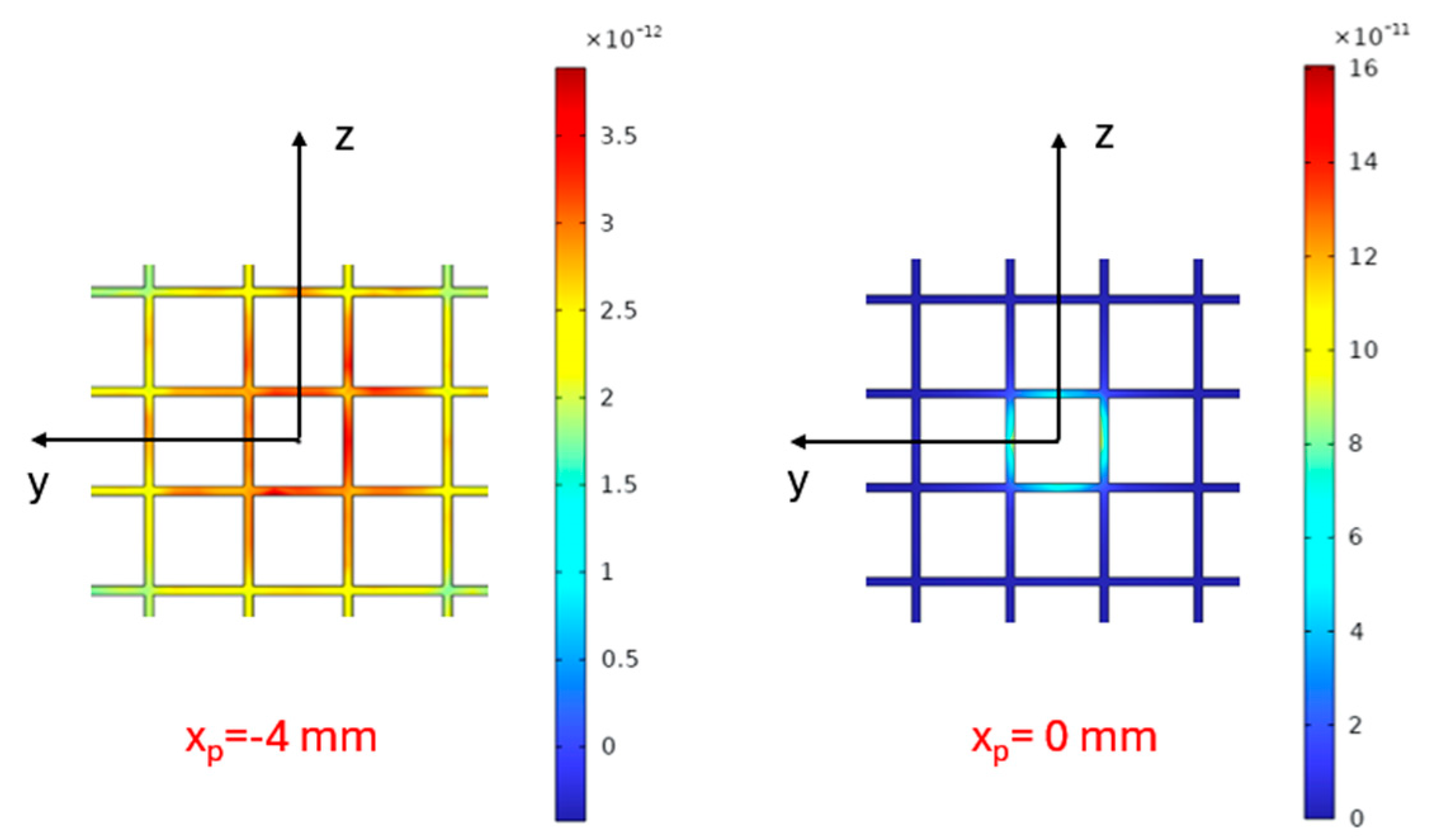
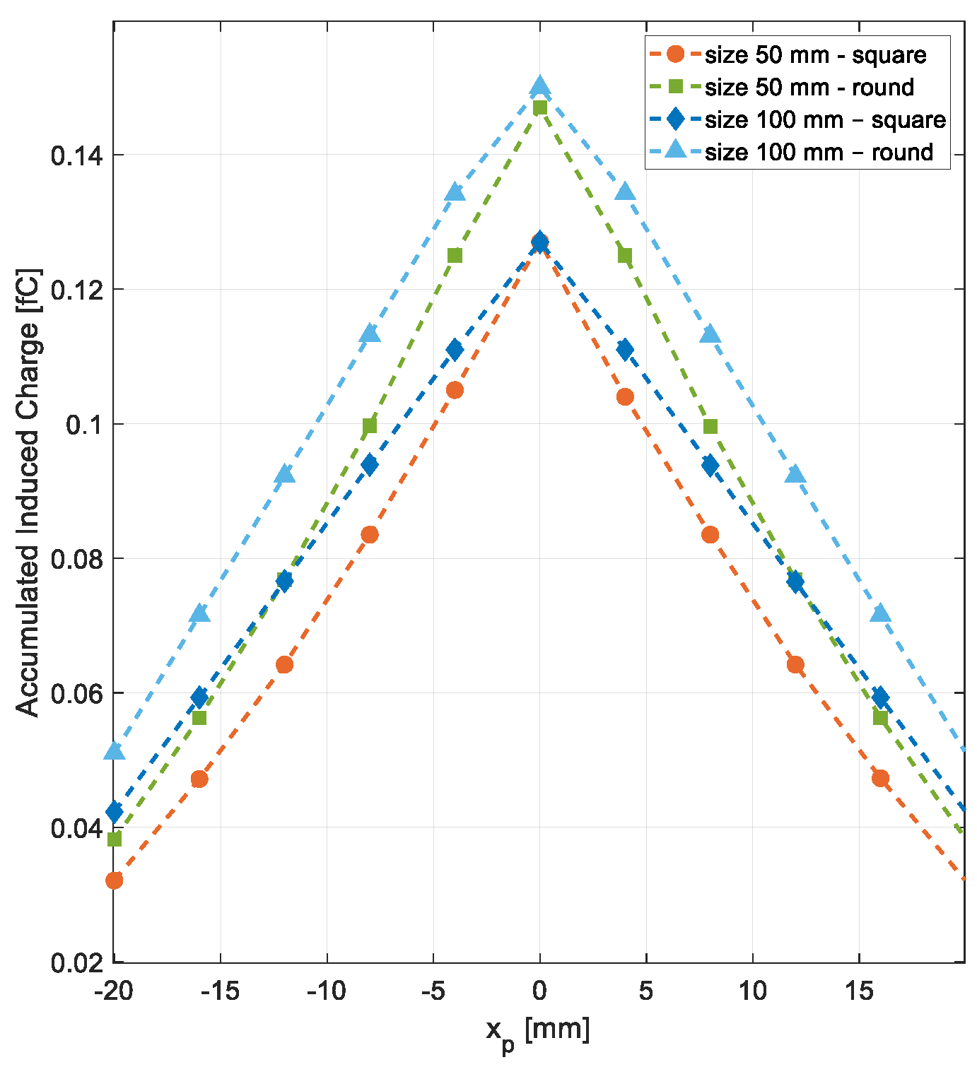
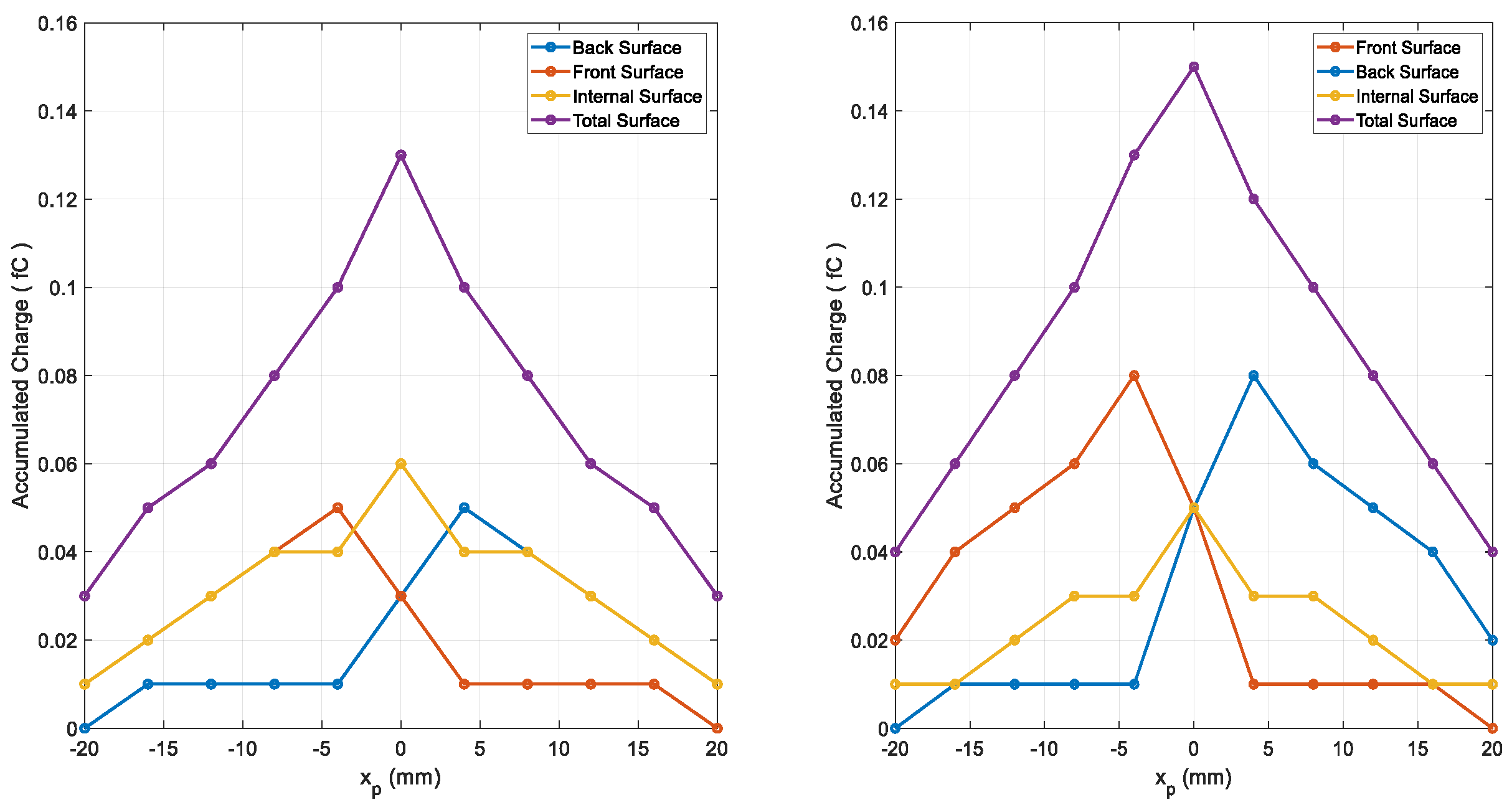
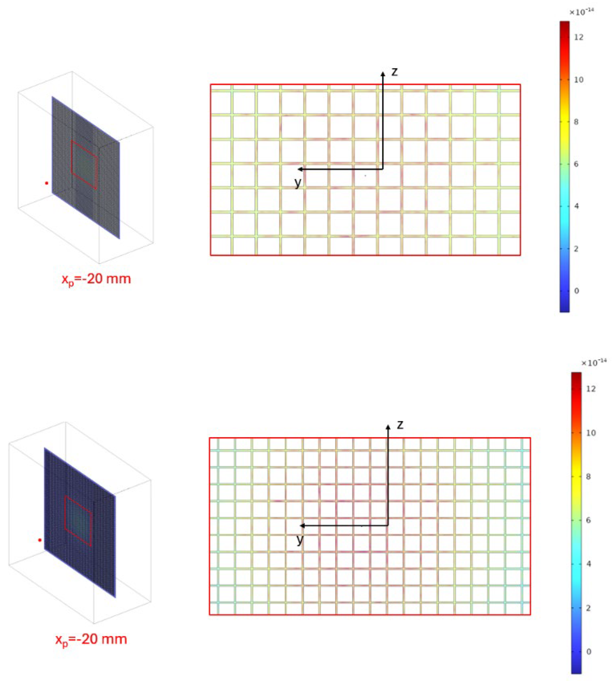
3.1.1. Electrostatic Performance

Figure 4 shows the charge surface density of the grids when the particle is at −20 mm distance, whereas Figure 5 shows a detailed view of the charge surface density for the grid with the square pattern when the particle is at −4 mm and 0 mm distances. Figure 6 shows the accumulated induced charge for the four configurations, obtained by integrating over the grid area, the charge surface density in each position of the charged particle.
Figure 7 shows the accumulated induced charge for the 50 × 50 mm configurations, providing the charge breakdown on the grid’s surfaces in each position of the charged particle.

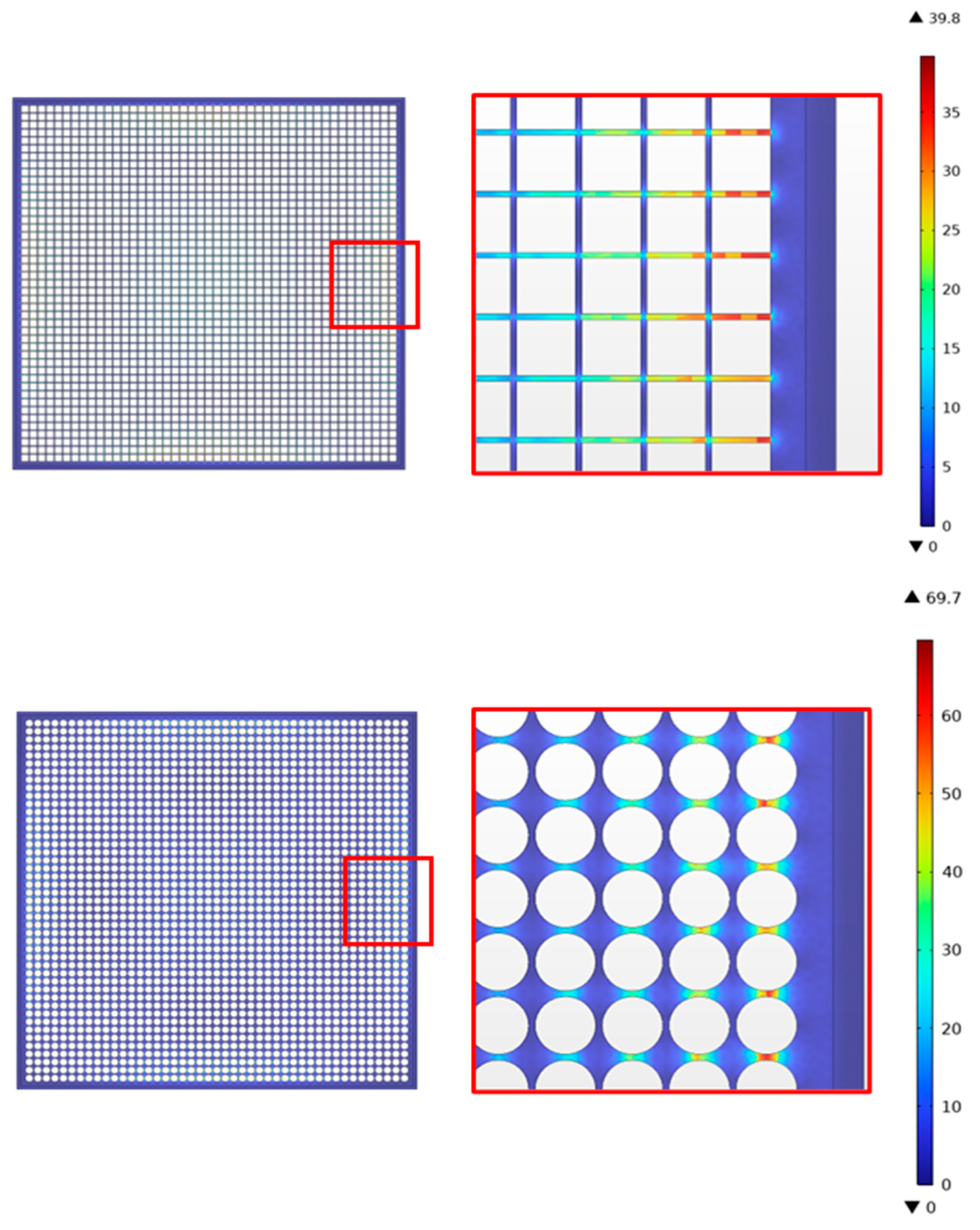
3.1.2. Modal Analysis

Table 1 summarises the computed resonances of the first five modes of vibration for the investigated configurations. The configurations that do not fulfil the dynamic behaviour design requirement are shown in red. Moreover, Figure 8 shows the first four modes of vibration of the grid (50 mm × 50 mm size and square pattern). The modal shapes shown in Figure 8 were also found in the other geometrical configurations, but at different frequencies.

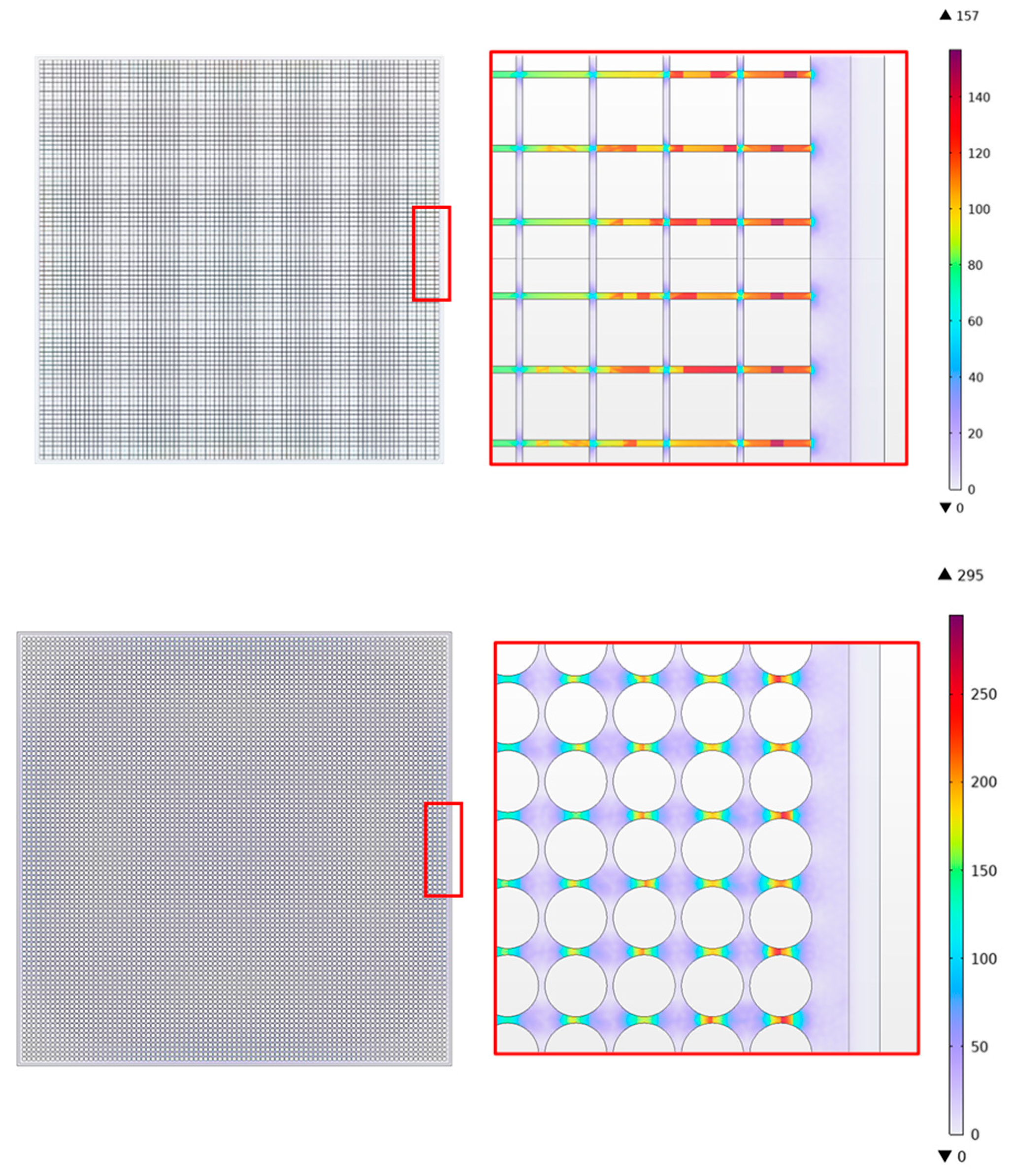
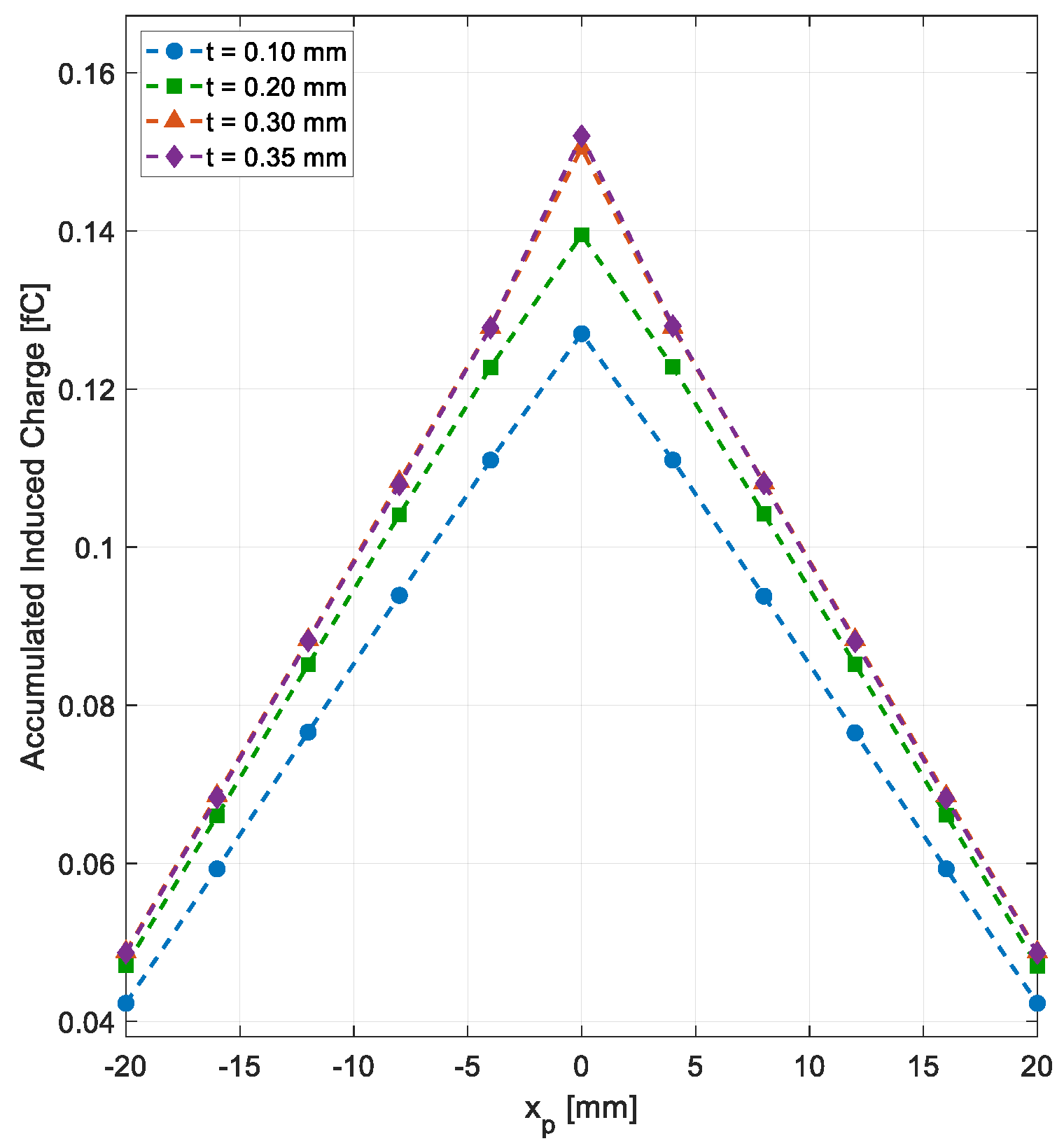
3.1.3. Quasi-Static Analysis

The Von Mises stresses distribution under vertical quasi-static acceleration is shown in Figure 9 and Figure 10, for the smaller- and larger-sized configurations, respectively.
The computed MOSs for the simulated conditions are given in Table 2.

3.2. Thickness Influence with Fixed Pattern and Geometry

In the following section, a comparison of the electrostatic and mechanical performance is reported, considering variable thickness but fixed grid geometry (size 100 mm × 100 mm, squared pattern).

3.2.1. Electrostatic Performance

To isolate the effect of grid thickness on induction and mechanical performance, the 100 mm square grid was simulated at four thicknesses (from 0.10 mm to 0.35 mm) while fixing the pattern and grid size. Figure 11 shows the induced charge density when the particle is at −20 mm from the grid, for the two extreme values of the investigated thickness, i.e., 0.1 mm and 0.35 mm, respectively. Figure 12 highlights the maximum charge density varying the particle position, considering the two extreme values of the grid thickness. Eventually, Figure 13 shows the accumulated charge integrated on the grid surface by varying the particle positions.

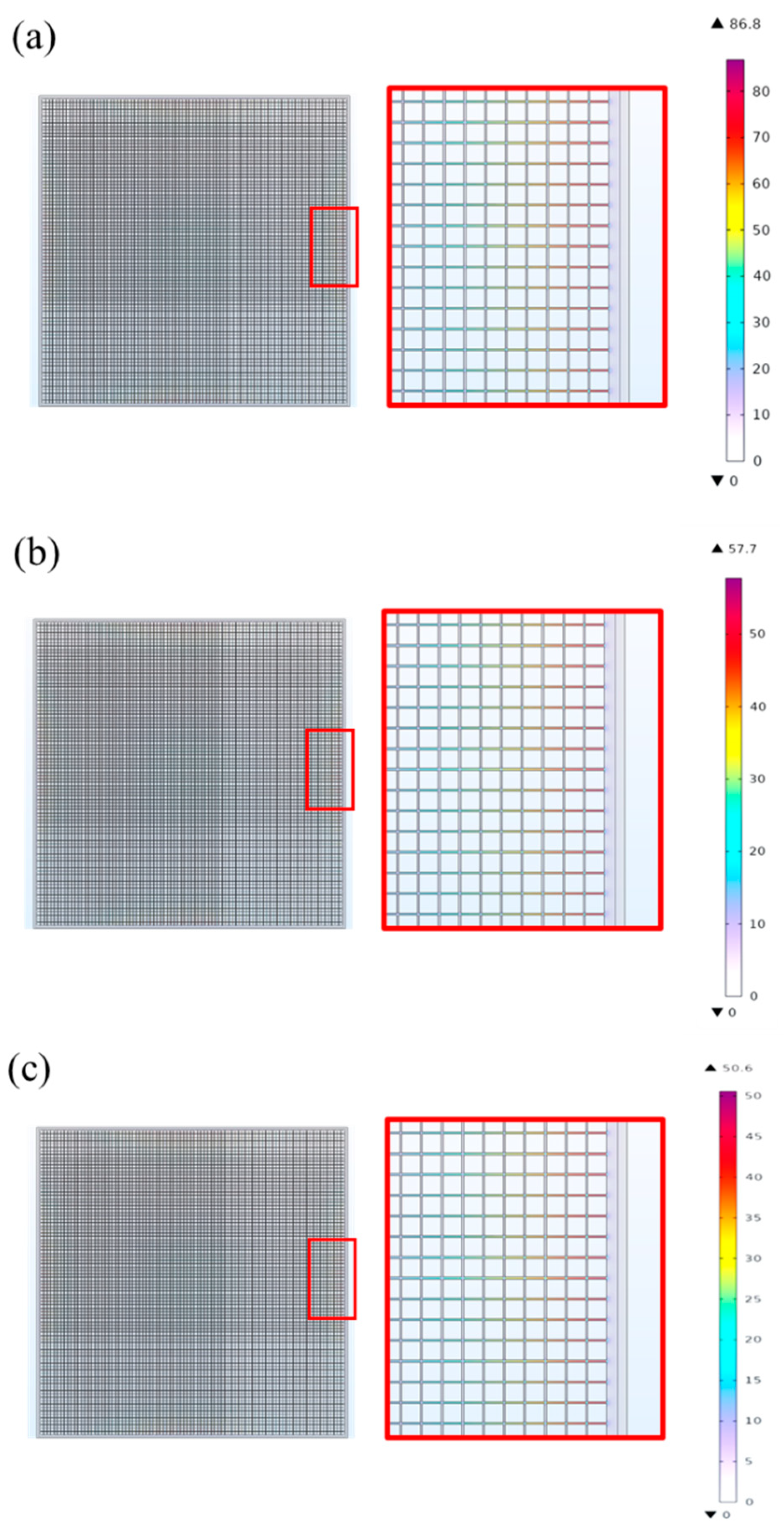
3.2.2. Modal Analysis

Table 3 summarises the computed resonances for the first five modes of vibration, varying the thickness from 0.1 mm to 0.35 mm. The configurations that do not fulfil the dynamic behaviour design requirement are shown in red.

3.2.3. Quasi-Static Analysis

In Figure 14, the stress distribution on the grid for the largest thickness is given. The maximum Von Mises stress and related MOSs for the tested configuration are summarised in Table 4.

3.3. Discussion

Numerical results showed that the grid configuration with a round pattern provides the best performance in accumulating an induced charge. As shown in Figure 6, considering the grid configurations with the largest size, the computed induced charge peak was about 1.50 × 10⁻¹⁶ C, i.e., 18% higher than the one obtained with the square pattern. By analysing the numerical outputs with the smaller size configuration, a similar result was achieved. The round pattern provided a maximum accumulated charge of about 1.47 × 10⁻¹⁶ C, i.e., 16% more than the square counterpart. On the other hand, no significant difference in the accumulated induced charge was found when analysing the effect on the electrical performance of the grid sizes. This is explained by the fact that the effect of the charge inductions is confined to a portion of the grid, i.e., in the central area for the simulated cases, as shown in Figure 4, Figure 5 and Figure 10; therefore, there is no advantage to increasing the size of the grid. Indeed, this depends on the specific position of the particle entering the instrument, which is aligned with the grid centre. Moving the particle to another position, or considering inclined trajectories, would lead to different results; indeed, as shown in Figure 5, the maximum of the induced charge, achieved when the particle position is at zero distance with respect to the grid, is well-confined in a very small area of a few cells of the grid where the particle passes through.
Increasing the surface of the grid where the particle induces the charge allows for improving the electrostatic performance. This is demonstrated by numerical results in Figure 7, where the breakdown of the induced charge on the surfaces of the grid (i.e., front, back, and internal surfaces) is shown, with respect to the overall charge, analysing the two investigated patterns for the 50 × 50 mm configuration. As it was found, all of the surfaces contribute to the overall charge, but the round pattern, having larger front and back surfaces compared to the square configuration, compensates for its smaller internal surface. The overall result is that the round pattern provides a better electrostatic performance, and in general, increasing the surface where the induced charge surface density is relevant allows for increasing the overall induced charge.
These findings are relevant to guide the overall LD GRIDS development, which aims to minimise the instrument size without jeopardising the overall performance. The grid size, which also accounts for the particle spatial distribution incoming to the DTS, can be selected by considering other design constraints, e.g., the ones posed by the mechanical and thermal environment.
Considering the mechanical performance, the larger size causes a reduction in the mechanical stiffness. As summarised in Table 1, the major reduction in the first natural frequencies of the grid was found passing from the smallest to the largest size. In fact, the largest size was shown to not be compliant with the dynamic requirement, given that most of the computed modes are lower than 150 Hz. The result is related to the thickness of the grid, set to 0.1 mm. In fact, the dynamic behaviour can be remarkably improved by increasing the thickness, as shown by the modal analysis summary in Table 3. A thickness value of 0.3 mm allows for the fulfilment of the design requirement, shifting the first resonance of the grid far from the dangerous low-frequency excitation range, experienced by the payload during the liftoff of the rocket. No significant effect from the grid pattern was noted, i.e., either the round or the square patterns provided similar dynamic results.
The mechanical resistance was assessed through the quasi-static analyses by considering a high quasi-static acceleration level normal to the grid. In general, the stress distribution shows the largest value near the constrained area, since the bending stiffness of the grid is involved in the deformation under the loading condition. This result is well-documented by Figure 9 and Figure 10. Von Mises stress is lower for the compact configuration, and, in general, it is lower for the square pattern. In fact, for the small-size grid, the maximum Von Mises stress is about 40 MPa and 70 MPa, for the square and circular patterns, respectively. By increasing the grid size, the peak stress increases accordingly, given that, with the same thickness, the compliance of the grid increases as well. Indeed, in the 100 mm × 100 mm configuration, the maximum Von Mises stress is about 157 MPa and 295 MPa, for the square and circular patterns, respectively. Similar to what was found for the dynamic behaviour, the mechanical resistance assessment was not positive for the largest size grid, given that the computed MOS for the circular pattern was negative. The obtained result is strongly affected by the grid thickness, set in these analyses to 0.1 mm. Increasing the grid thickness allowed for stress reduction, as shown by the numerical results in Table 4 and Figure 14, which showed a marked reduction of about one-third of the maximum Von Mises stress value at the maximum thickness (i.e., 0.35 mm). This trend was not assessed for the round pattern, but a similar result is expected, since the grid thickness mainly affects either the static or dynamic stiffnesses; therefore, its increase provides a beneficial reduction of the bending and, consequently, of the maximum stress and deformation.
As a result of analysing the numerical results of the electrostatic performance and varying the grid thickness, shown in Figure 11, Figure 12 and Figure 13, it can be stated that increasing the grid thickness allows for a better performance. In fact, the thicker the grid, the larger the contribution of the internal surface is to the accumulated charge, e.g., the configuration with 0.35 mm thickness provides approximately 1.52 × 10⁻¹⁶ C charge, about 22% higher than the same grid with the lowest thickness (maximum computed value of 1.25 × 10⁻¹⁶ C). The maximum induced surface charge density (units C/m2) reduces with the thickness, as shown in Figure 12, but the reduction is not detrimental to the overall performance of the grid. This is a relevant result as well, because it suggests that increasing the grid thickness within the investigated range allows for a better electrostatic performance, which is in agreement with the results obtained from the mechanical assessment.
Summarising the findings of the study, the combination of the footprint size and thickness primarily dominates the mechanical resistance and modal behaviour, and generally, reducing the size and increasing the grid’s thickness allows for a better mechanical performance. Considering the electrostatic behaviour, the round pattern showed a higher induced charge, a relevant parameter to be maximised to enhance the sensitivity of the dust analyser. Moreover, the possibility of increasing the thickness of the grid within the investigated range has a beneficial effect on the induced charge and the mechanical resistance, allowing for optimisation of the overall size of the LD GRIDS and paving the way for developing compact and miniaturised space dust analysers, targeting lunar exploration.
As the design is developed further, the definition of the mission requirements for the lunar application shall be completed to provide a more detailed scenario in which to complete the design, considering, for instance, the temperature environment to be overcome with the developed instrument. Moreover, the effect of the void/available surface of the identified pattern on the instrument sensitivity, as well as the particle size distribution or the particle trajectories, will be assessed as a future development of this work to optimise the overall instrument performance.

4. Conclusions

The work provided a systematic evaluation of the key design parameters of the sensing elements for the Lunar Dust GRID System (LD GRIDS). By leveraging multiphysics modelling software, the study assessed the impact of grid pattern, size, and thickness on the sensor’s electrostatic performance, dynamic response, and structural integrity under high acceleration levels and quasi-static loading. Grids with round patterns yield a higher induced charge compared to square grids, but also to localised stresses under high-g loading. Improvement of the mechanical resistance was achieved by increasing the grid thickness and design leverage, which also reduced the maximum Von Mises stresses and improved the dynamic responses of the sensing element. The electrostatic performance showed beneficial results by improving the thickness of the grid, due to a general increase in the surface area effectively interested by the induced charge. The findings offer a comprehensive framework for optimising the LD GRIDS sensing elements, enabling the design of a sensor that achieves an optimal balance between the electrostatic induction performance and mechanical resistance, targeting lunar dust detection for the next missions to the Moon. Future work will focus on experimental validation of the obtained results and detailed sensor design, aiming to manufacture and characterise an equivalent engineering model in a relevant environment for the intended application.

Author Contributions

Conceptualization, D.S. and A.M.R.M.A.; methodology, D.S., A.M.R.M.A. and C.P.; software, A.M.R.M.A.; validation, D.S., A.M.R.M.A., A.A., B.S., C.P. and F.E.; formal analysis, D.S., A.M.R.M.A., A.A., B.S., C.P. and F.E.; investigation, D.S., A.M.R.M.A., A.A. and F.E.; writing—original draft, A.M.R.M.A.; writing—review and editing, D.S., A.A., B.S., C.P. and F.E.; visualization, A.M.R.M.A.; supervision, D.S. All authors have read and agreed to the published version of the manuscript.

Funding

The research activities described in this paper were carried out with the contribution of the Next Generation EU funds within the National Recovery and Resilience Plan (PNRR), Mission 4—Education and Research, Component 2—From Research to Business (M4C2), Investment Line 3.1—Strengthening and creation of Research Infrastructures, Project IR0000038—“Earth Moon Mars (EMM)”. EMM is led by INAF in partnership with ASI and CNR.

Data Availability Statement

Dataset available on request from the authors.

Conflicts of Interest

The authors declare no conflict of interest.

References

  1. Creech, S.; Guidi, J.; Elburn, D. Artemis: An Overview of NASA’s Activities to Return Humans to the Moon. In Proceedings of the 2022 IEEE Aerospace Conference (AERO), Big Sky, MT, USA, 5–12 March 2022; pp. 1–7. [Google Scholar] [CrossRef]
  2. Smith, M.; Craig, D.; Herrmann, N.; Mahoney, E.; Krezel, J.; McIntyr, N.; Goodliff, K. The Artemis Program: An Overview of NASA’s Activities to Return Humans to the Moon. In Proceedings of the 2020 IEEE Aerospace Conference, Big Sky, MT, USA, 7–14 March 2020; pp. 1–10. [Google Scholar] [CrossRef]
  3. Auer, S.; Grün, E.; Kempf, S.; Srama, R.; Srowig, A.; Sternovsky, Z.; Tschernjawski, V. Characteristics of a dust trajectory sensor. Rev. Sci. Instrum. 2008, 79, 084501. [Google Scholar] [CrossRef] [PubMed]
  4. Grün, E.; Srama, R.; Altobelli, N.; Altwegg, K.; Carpenter, J.; Colangeli, L.; Glassmeier, K.-H.; Helfert, S.; Henkel, H.; Horanyi, M. DuneXpress. Exp. Astron. 2009, 23, 981–999. [Google Scholar] [CrossRef]
  5. Xie, J.; Sternovsky, Z.; Grün, E.; Auer, S.; Duncan, N.; Drake, K.; Le, H.; Horanyi, M.; Srama, R. Dust trajectory sensor: Accuracy and data analysis. Rev. Sci. Instrum. 2011, 82, 105104. [Google Scholar] [CrossRef] [PubMed]
  6. Xie, J.; Sternovsky, Z.; Auer, S.; Drake, K.; Grün, E.; Horanyi, M.; Le, H.; Srama, R. Laboratory testing and data analysis of the Electrostatic Lunar Dust Analyzer (ELDA) instrument. Planet. Space Sci. 2013, 89, 63–70. [Google Scholar] [CrossRef]
  7. Srama, R.; Ahrens, T.J.; Altobelli, N.; Auer, S.; Bradley, J.G.; Burton, M.; Dikarev, V.V.; Economou, T.; Fechtig, H.; Görlich, M.; et al. The Cassini Cosmic Dust Analyzer. Space Sci. Rev. 2014, 114, 465–518. [Google Scholar] [CrossRef]
  8. Auer, S.; Grün, E.; Srama, R.; Kempf, S.; Auer, R. The charge and velocity detector of the cosmic dust analyzer on Cassini. Planet. Space Sci. 2002, 50, 773–779. [Google Scholar] [CrossRef]
  9. Horanyi, M.; Sternovsky, Z.; Lankton, M.; Dumont, C.; Gagnard, S.; Gathright, D.; Wright, G. The lunar dust experiment (LDEX) onboard the lunar atmosphere and dust environment explorer (LADEE) mission. In The Lunar Atmosphere and Dust Environment Explorer Mission (LADEE); Springer: Cham, Switzerland, 2015; pp. 93–113. [Google Scholar]
  10. Sommer, M.; Li, Y.; Srama, R.; Simolka, J.; Strack, H.; Gläser, J.; Arai, T. Measuring micro-debris In-Situ with the DESTINY+ dust analyzer. In Proceedings of the 2nd NEO and Debris Detection Conference, Darmstadt, Germany, 24–26 January 2023; p. 37. [Google Scholar]
  11. Scaccabarozzi, D.; Ahmed, A.M.R.; Saggin, B.; Esposito, F.; Porto, C.; Mongelluzzo, G. Feasibility Design of LD GRIDS, a Dust Analyzer for the Moon. In Proceedings of the 2024 11th International Workshop on Metrology for AeroSpace (MetroAeroSpace), Lublin, Poland, 3–5 June 2024; pp. 427–431. [Google Scholar] [CrossRef]
  12. Rezinkina, M.; Braxmaier, C. Designs of Miniature Optomechanical Sensors for Measurements of Acceleration with Frequencies of Hundreds of Hertz. Designs 2024, 8, 67. [Google Scholar] [CrossRef]
  13. Mejía Rodríguez, M.; González-Estrada, O.A.; Villegas-Bermúdez, D.F. Finite Element Analysis of Patient-Specific Cranial Implants under Different Design Parameters for Material Selection. Designs 2024, 8, 31. [Google Scholar] [CrossRef]
  14. Al-Haddad, L.A.; Jaber, A.A.; Giernacki, W.; Khan, Z.H.; Ali, K.M.; Tawafik, M.A.; Humaidi, A.J. Quadcopter unmanned aerial vehicle structural design using an integrated approach of topology optimization and additive manufacturing. Designs 2024, 8, 58. [Google Scholar] [CrossRef]
  15. Cecere, G.; Irimescu, A.; Merola, S.S. System Design and Stress–Strain Analysis for Cranking and Motoring Small-Size Engines. Designs 2024, 8, 14. [Google Scholar] [CrossRef]
  16. Scaccabarozzi, D.; Martina, C.; Saggin, B.; Vieira Vaz, E.; Palomba, E.; Longobardo, A.; Gisellu, C.; Dirri, F.; Zampetti, E.; Pedone, M. Feasibility Design of DIANA, a Dust Analyzer developed for the Tianwen-2 Mission. In Proceedings of the 2024 11th International Workshop on Metrology for AeroSpace (MetroAeroSpace), Lublin, Poland, 3–5 June 2024; pp. 422–426. [Google Scholar] [CrossRef]
  17. Scaccabarozzi, D.; Saggin, B.; Magni, M.; Valnegri, P.; Corti, M.G.; Palomba, E.; Longobardo, A.; Dirri, F.; Zampetti, E. Design of 3D printed holder for quartz crystal microbalances. In Proceedings of the 2021 IEEE 8th International Workshop on Metrology for AeroSpace (MetroAeroSpace), Naples, Italy, 23–25 June 2021; pp. 715–719. [Google Scholar] [CrossRef]
Figure 1. (Left) FE model of the case study and (right) comparison between the induced charge in the developed model and the one from the literature [3].
Designs 09 00070 g001
Figure 2. (Left) 3D electrostatic FE model of LDS-GRIDS and (right) two investigated round and square patterns.
Designs 09 00070 g002
Figure 3. Grid meshed model: in green colour the constrained sides are shown, whereas the red area shows a detailed view of the mesh (geometrical model 100 × 100 mm, thickness 0.1 mm).
Designs 09 00070 g003
Figure 4. Computed induced charge distribution (units C/m2) for the two grids’ shapes: (top) 50 × 50 mm grid size, square pattern, and (bottom) 50 × 50 mm grid size, round pattern, particle distance −20 mm.
Designs 09 00070 g004
Figure 5. Computed induced charge distribution (units C/m2) for the 50 × 50 mm grid size, square pattern, at different particle positions: (left) xp = −4 mm and (right) xp = 0 mm.
Designs 09 00070 g005
Figure 6. Accumulated charge (units fC) computed from different grid configurations, induced by the particle moving along the normal trajectory, from −20 mm to 20 mm.
Designs 09 00070 g006
Figure 7. Accumulated charge breakdown on the grid’s surfaces (Front, Back, Internal, and Total) varying the particle position xp: (left) square pattern, 50 × 50 mm size, and (right) round pattern, 50 × 50 mm size.
Designs 09 00070 g007
Figure 8. Contour plots of the adimensional displacement of the modal analysis: (a) 1st, (b) 2nd, (c) 3rd, and (d) 4th mode of vibration, 50 mm × 50 mm and square pattern.
Designs 09 00070 g008
Figure 9. Stress distribution (along with a detailed view) for both the square and round patterns, with the smaller grid size, under the quasi-static loading: (top) square and (bottom) round patterns. Units are MPa.
Designs 09 00070 g009
Figure 10. Stress contour (along with a zoomed view) for both the square and round patterns, with a similar grid size (100 mm), under quasi-static loading: (top) square and (bottom) round patterns. Units are MPa.
Designs 09 00070 g010
Figure 11. Distribution of the induced charge density (units C/m2) with thicknesses at 0.1 mm and 0.35 mm, while fixing the pattern (square) and the grid size (100 mm). Particle distance at −20 mm.
Designs 09 00070 g011
Figure 12. Induced maximum charge density (fC/m2) with thicknesses at 0.1 mm and 0.35 mm, while fixing the pattern (square) and the grid size (100 mm).
Designs 09 00070 g012
Figure 13. Accumulated induced charge changing the thickness from 0.1 mm to 0.35 mm, while fixing the pattern (square) and the grid size (100 mm).
Designs 09 00070 g013
Figure 14. Stress contour (along with a detailed view) for the square pattern, with a grid size of 100 mm and different thicknesses, under the quasi-static loading in the vertical direction: (a) 0.2 mm, (b) 0.3 mm, and (c) 0.35 mm. Units are MPa.
Designs 09 00070 g014
Table 1. First Five Natural Frequencies (Hz) t = 0.1 mm. The red colour highlights configurations which do not fulfil the dynamic requirement.
Mode50 mm Size
(Square Pattern)
50 mm Size
(Round Pattern)
100 mm Size
(Square Pattern)
100 mm Size
(Round Pattern)
1245.3250.763.163.8
2501.7511.4129.1130.2
3501.7511.8186.9130.2
4726.5751.7233.3191.0
5906.5918.7234.3233.9
Table 2. Quasi-static analyses: computed maximum stress and related MoSs.
50 mm Size (Square Pattern)50 mm Size (Round Pattern)100 mm Size (Square Pattern)100 mm Size
(Round Pattern)
Maximum
Stress (MPa)
4070157295
MOS4.522.150.4−0.25
Table 3. First Five Natural Frequencies (units Hz) for 100 mm square mesh at different grid thicknesses.
Modet = 0.1 mmt = 0.2 mmt = 0.3 mmt = 0.35 mm
163.1119.1174.6202.3
2129.1245.3360.5418.1
3186.9245.3360.6418.1
4233.3341.1492.9568.9
5234.3451.4668.1776.2
Table 4. Quasi-static analyses computed Von Mises stress and related MoSs.
t = 0.1 mmt = 0.2 mmt = 0.3 mmt = 0.35 mm
Maximum Stress (MPa)15786.857.750.6
MOS0.41.542.833.36
Disclaimer/Publisher’s Note: The statements, opinions and data contained in all publications are solely those of the individual author(s) and contributor(s) and not of MDPI and/or the editor(s). MDPI and/or the editor(s) disclaim responsibility for any injury to people or property resulting from any ideas, methods, instructions or products referred to in the content.

