1. Introduction
Due to population development and industrialization, there is a huge increase in the need for electrical energy, and fossil fuels continue to be the most popular energy source despite their role in global warming [
1]. To address the challenges posed by the increasing energy demand and the environmental impact of fossil fuels, the concept of positive energy districts (PEDs) has emerged as a transformative solution [
2]. PEDs are urban areas designed to produce more energy than they consume by leveraging local renewable energy sources, smart grids, and energy storage systems [
3]. By prioritizing sustainability, PEDs aim to contribute to the global energy transition by reducing carbon emissions, enhancing energy efficiency, and promoting decentralized energy management [
4]. One of the critical technologies enabling energy optimization in PEDs is the DC–DC converter. DC–DC converters play a fundamental role in managing the energy generated from various renewable sources, such as solar photovoltaic (PV) panels, and coordinating energy storage systems, like batteries. By efficiently converting DC voltages to match the needs of different energy components within the district, these converters help minimize energy losses and enhance overall system efficiency. Nevertheless, the utilization of fossil fuels poses environmental concerns, making alternative sources like solar energy increasingly attractive due to its inherent noise-free and environmentally friendly characteristics [
5]; this is while the efficiency of photovoltaic (PV) panels is significantly influenced by factors such as sun exposure, temperature variations, and shadow fluctuations [
6].
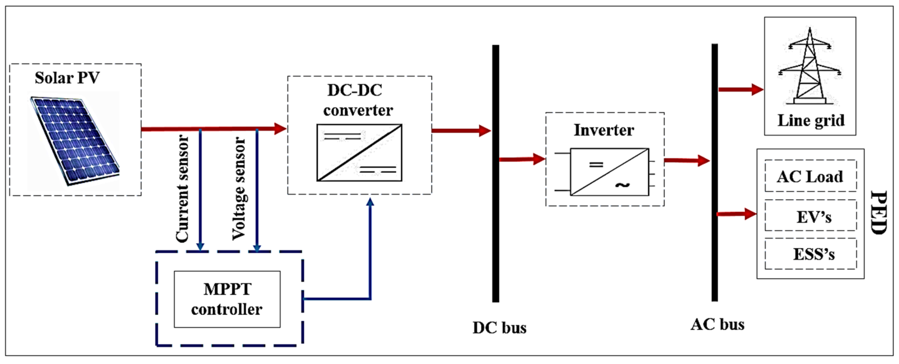
This study’s objective is fully consistent with the positive energy district (PED) concept, which seeks to achieve a positive energy balance. A conventional solar energy harvesting system comprises key components, such as a photovoltaic (PV) array, a maximum power point tracking (MPPT) controller, as well as a DC–DC converter, a battery, a load (AC/DC), and an inverter, as illustrated in
Figure 1 [
7]. To cater to the voltage requirements of the load, intermediate circuits, such as DC–DC converters, are crucial for transforming the low direct current (DC) output voltage from a solar photovoltaic (PV) energy-producing system into a voltage that is appropriate for use [
8]. Some of the rectifiers’ problems, such as harmonics, are passed on to the DC–DC converters. Implementing active power filters solves this issue [
9]. The power converters also include a controller that is set up to manage the switching of the many switching units [
10]. Peripheral pulse-width modulated (PWM) boost converters have facilitated the development of switched-mode DC–DC converters aimed at producing output DC voltages greater than the input DC voltage. These setups use magnetic field storage components, like inductors, or electric field storage components, like capacitors, with active or passive switching elements to temporarily store and distribute energy from the input [
11,
12].
In response to the drawbacks of conventional PWM boost converters, considerable efforts have been devoted to alleviating these limitations through non-isolated high step-up DC–DC converters (NHSDCs) [
13]. These converters can be categorized into isolated and non-isolated types. Isolated converters, featuring electrical separation between input and output using transformers, offer protection against high-power flows [
14]. However, they come with drawbacks, such as transformer core saturation, increased component count, and lower efficiency, particularly within applications requiring low and medium power [
15,
16]. Conversely, non-isolated DC–DC converters, lacking a transformer, boast fewer components, reduced energy loss, and a smaller overall size [
17]. Utilizing strategies like interleave boost (IB), coupled inductor (CI), switched capacitor (SC), cascaded boost (CB), switched inductor (SI), and voltage multiplier (VM), a number of non-isolated topologies have surfaced in recent years to achieve high step-up voltage gains [
18]. These topologies change the duty ratio in an effort to get high-voltage gains [
19].
Earlier, the switch voltage stress in DC–DC boost converters was equivalent to the output voltage, necessitating the use of high-rating switches. This requirement significantly increased conduction losses and restricted the achievable voltage gain. To overcome these limitations, researchers introduced advanced non-isolated DC–DC converters with higher voltage gains, expressed by the relation (1 + δ)/ (1 − δ), where δ represents the duty ratio of the switch [
20]. These converters allow for improved performance by reducing switch stress and enhancing energy conversion efficiency. However, despite these advancements, there remains a substantial scope for further improvements, particularly in developing high step-up DC–DC converters with better efficiency, higher voltage gain, and reduced component count.
In response to these challenges, Kumaravel Sundaramoorthy et al. [
21] proposed a novel single switching impedance network (SSIN)-based converter. This topology offers the advantage of structural scalability, allowing for an extension with multiple stages (n-stage), which increases the number of diodes and inductors by 3(1 + n) and 1 + n, respectively. The key innovative aspects of this paper include:
New Topology: The SSIN converter topology is unique, offering a design that achieves higher or more efficient voltage conversion with a single switch, potentially simplifying circuitry and reducing cost.
Dual-Mode Operation Analysis: The study covers both continuous and discontinuous conduction modes, providing a comprehensive understanding of the converter’s operation across different load conditions.
Impact of Parasitic Elements: By analyzing how parasitic elements affect the converter’s DC voltage gain and efficiency, the paper addresses real-world performance considerations, enhancing the converter’s practical applicability.
However, while this work introduces a valuable contribution to converter design, it does not explicitly address key challenges, such as stability in grid-connected systems or the integration of MPPT controllers under fault conditions. Our study builds upon this foundation by simulating a grid-connected PV system that incorporates MPPT and a three-level inverter for enhanced energy management. Furthermore, we introduce and analyze the system’s response to short-circuit faults to assess the converter’s stability and suitability for real-world renewable energy systems. The ability to integrate MPPT and maintain system stability during fault conditions is critical for optimizing the performance of grid-connected PV systems. This becomes especially important in the context of PEDs, where energy efficiency, reliability, and seamless integration with renewable energy sources are paramount.
By simulating a grid-connected PV system that incorporates MPPT and a 3-level inverter for improved energy management, and introducing and analyzing the system’s response to two short-circuit faults, this study aims to evaluate the converter’s stability and its suitability for real-world renewable energy systems. The ability to integrate MPPT and maintain system stability in fault conditions is crucial for optimizing the performance of grid-connected PV systems, particularly in the context of PEDs, where energy efficiency and reliability are paramount.
The application of advanced control strategies to the proposed converter highlights its superior performance and robustness in maintaining output voltage stability under varying conditions. In the context of the converter proposed for optimizing photovoltaic systems, control strategies refer to the methodologies and algorithms deployed to regulate and optimize the converter’s operation. These strategies are designed to achieve critical objectives, such as maximizing energy conversion efficiency, maintaining stability in output voltage or current despite fluctuations in photovoltaic input (e.g., shading or varying solar irradiance), and dynamically tracking the MPPT to ensure optimal energy extraction under all conditions. Additionally, advanced control approaches ensure robust performance by adapting to environmental variations like temperature changes, minimizing output ripple to enhance reliability, and safeguarding connected loads. Techniques such as feedback loops, PID controllers, model predictive control (MPC), and artificial intelligence (e.g., neural networks for MPPT optimization) are employed to implement these strategies effectively. These advanced control methods enable the converter to efficiently manage energy flow in photovoltaic systems, making them particularly suitable for integration into PEDs where reliability, efficiency, and seamless integration with renewable energy sources are crucial.
The format of this document is as follows: After a brief overview of PV systems and converter topology in
Section 1,
Section 2 describes how to operate the recommended SSIN converter. The SSIN converter’s design element is presented in
Section 3.
Section 4 presents the comparative simulation results, which highlight the superiority of the proposed converter and
Section 5 describes the discussion and comparison. The article is concluded in
Section 6.
2. Functioning of the Converter
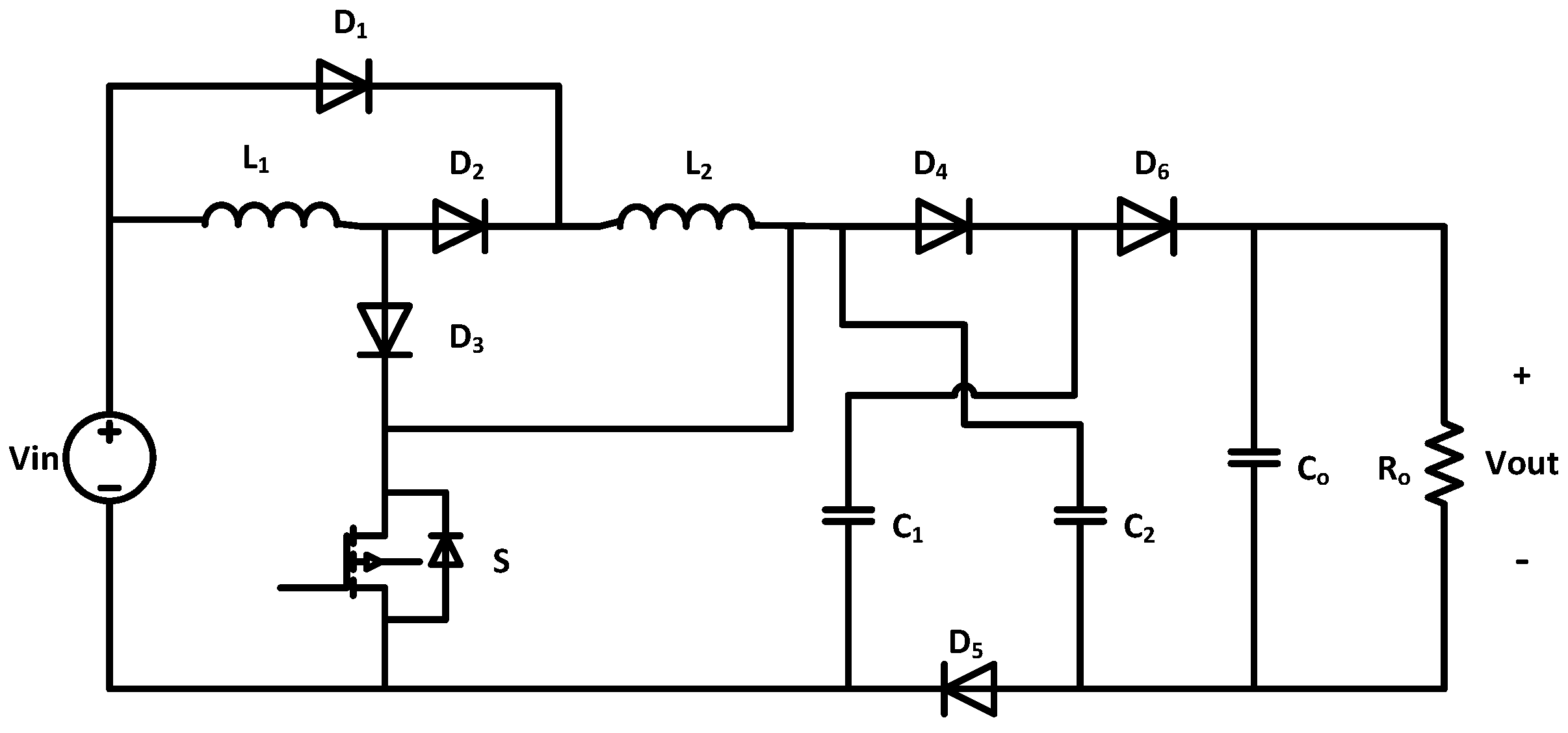
The operation of the proposed one-stage converter, depicted in
Figure 2, involves the interaction of several components: a single semiconductor switch, six diodes, two inductors (L
1 and L
2), and three capacitors (C
1, C
2, and an additional one). When the switch S is turned on, inductors L
1 and L
2 are charged by the input source. The energy stored in the inductors is transferred to the cross-connected capacitors C
1 and C
2 when the switch is turned off. These capacitors act as a voltage doubler, thereby enhancing the voltage boost achieved by the converter. This design facilitates efficient energy conversion and voltage amplification.
To understand the fundamental working concept of one-stage high step-up DC–DC converter, the following procedures are given [
21]:
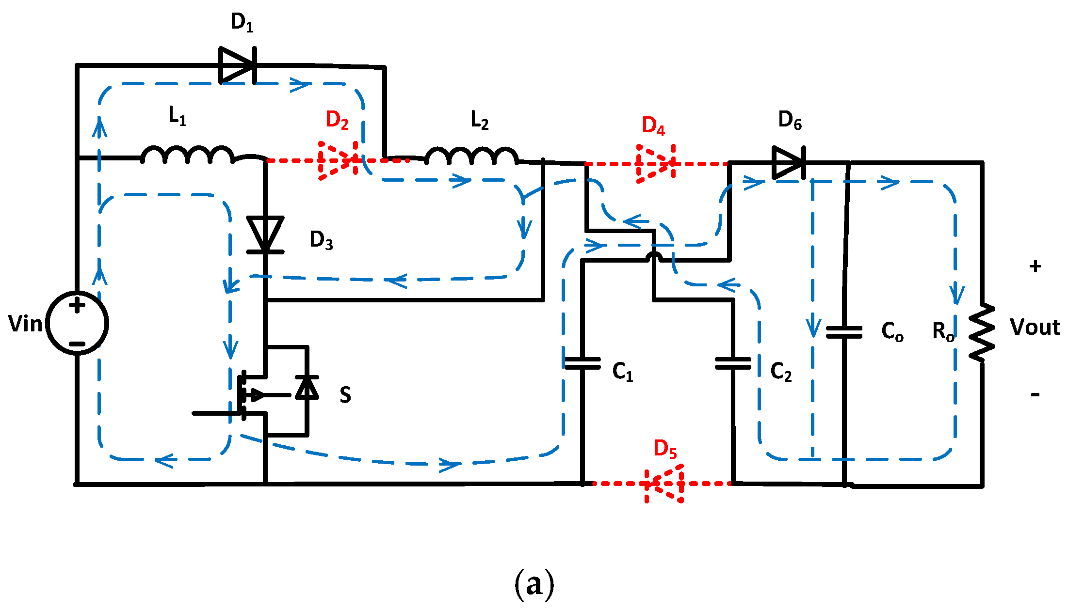
As shown in
Figure 3a, in Mode 1, this operating mode appears when:
Switch S On: For the interval 0 < t ≤ δTs, the switch S is closed.
Diodes Forward Biased: D1, D3, and D6.
Diodes Reverse Biased: D2, D4, and D5.
Inductors Charging: Input voltage Vin charges L1 and L2 in parallel.
Energy Supply: Capacitors C1 and C2 supply energy to the output capacitor Co and the load.
Voltage Across Inductors: Vin.
The output voltage of the load is the summation of the voltages provided by the voltage between the cross-connected capacitors as V0 = VC1 + VC2.
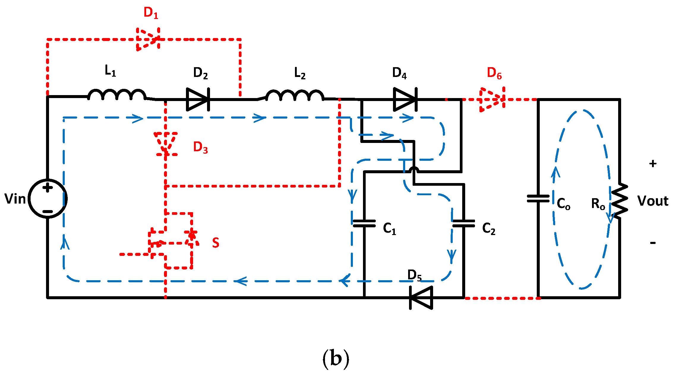
As shown in
Figure 3b, in Mode 2, this operating mode appears when:
Switch S Off: For δTs ≤ t < (1 − δ) Ts, the switch S is open.
Diodes Forward Biased: D2, D4, and D5.
Diodes Reverse Biased: D1, D3, and D6.
Inductors Discharging: L1 and L2 discharge energy into capacitors C1 and C2, which are cross connected, in series. The inductors L1 and L2 release their stored energy into the cross-connected capacitors in a series configuration.
Voltage Across Capacitors: At steady-state, VC1 = VC2 = Vout/2.
As illustrated in
Figure 3b, the voltage between inductors L
1 and L
2 is given by (1) when the output voltage is equal to the capacitor voltage:
The average voltage of the inductor is zero according to the volt-second balance of the inductor L1, as stated:
By solving Equation (3), the DC voltage gain for the converter operating in continuous conduction mode (CCM) is derived as follows:
4. Simulation Result
4.1. Comparison of Converter Performance
In this section, the simulation results for boost converters as a various type of non-isolated converters for solar PV panels integrated through VDC micro grids are presented and compared.
The simulated circuit of the high step-up DC–DC converter in one stage, based on the converter specification given in
Table 1, is shown in
Figure 4.
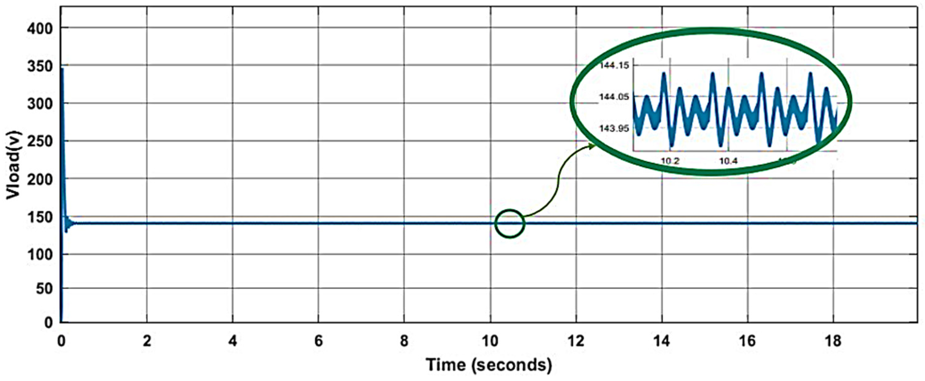
For Vin = 24 and duty cycle (δ = 0.5), it was calculated that the gain of this converter will result in an output voltage of 144. The output voltage plot of this converter is depicted in
Figure 5. This output voltage typically reflects how well the converter regulates the voltage level after converting it from the input source, and it also indicates the converter’s efficiency in maintaining a stable output.
The simulated circuit of the high volDC–DC converter is shown in
Figure 6.
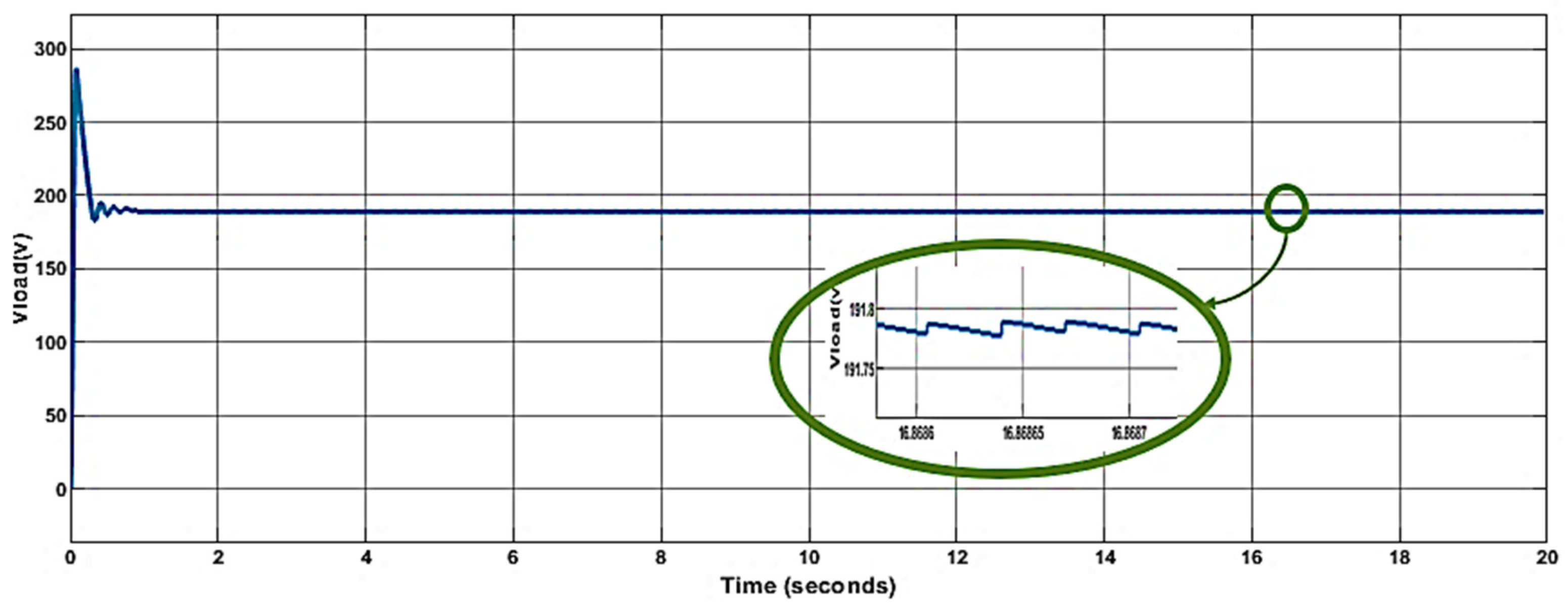
The output voltage of the double-stage high step-up DC–DC converter is shown in
Figure 7, which also indicates the converter’s efficiency in maintaining a stable output.
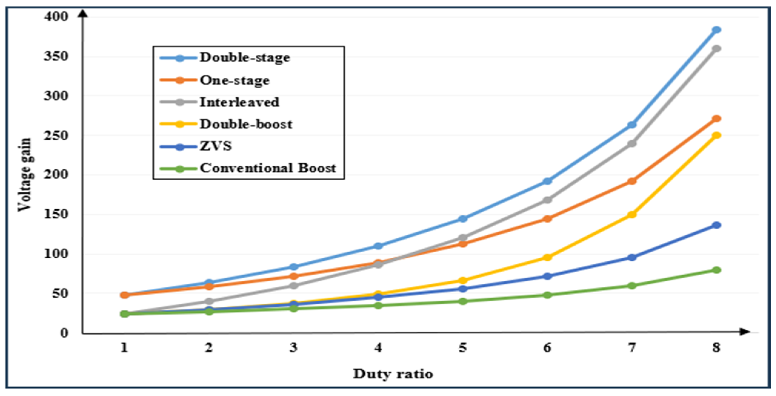
The comparative DC voltage gain for different configurations from previous works [
22,
23,
24,
25,
26,
27,
28,
29,
30] are shown in
Figure 8. In comparison to other documented converters, the suggested SSIN converter in its double-stage configuration offers a significantly higher voltage gain, as illustrated in the figure. This improvement is particularly evident at higher duty cycles, where the voltage gain increases substantially due to the optimized design of the converter. The double-stage architecture effectively combines the benefits of enhanced energy transfer and reduced losses, allowing the converter to achieve superior performance under demanding operating conditions.
At higher duty cycles, the system leverages the extended range of energy conversion, enabling greater output voltage levels without compromising efficiency. This feature makes the SSIN converter particularly suitable for applications requiring high-voltage gains, such as photovoltaic systems and other renewable energy integrations, where achieving maximum power extraction and system scalability are critical.
In
Table 2, five different boost topologies were compared. As can be seen, the n-stage (n = 1.2) has a reasonable complexity and a high-voltage gain, making it a good candidate to use with low voltage DC sources, such as ultra-capacitors, solar PV, fuel cells, and batteries.
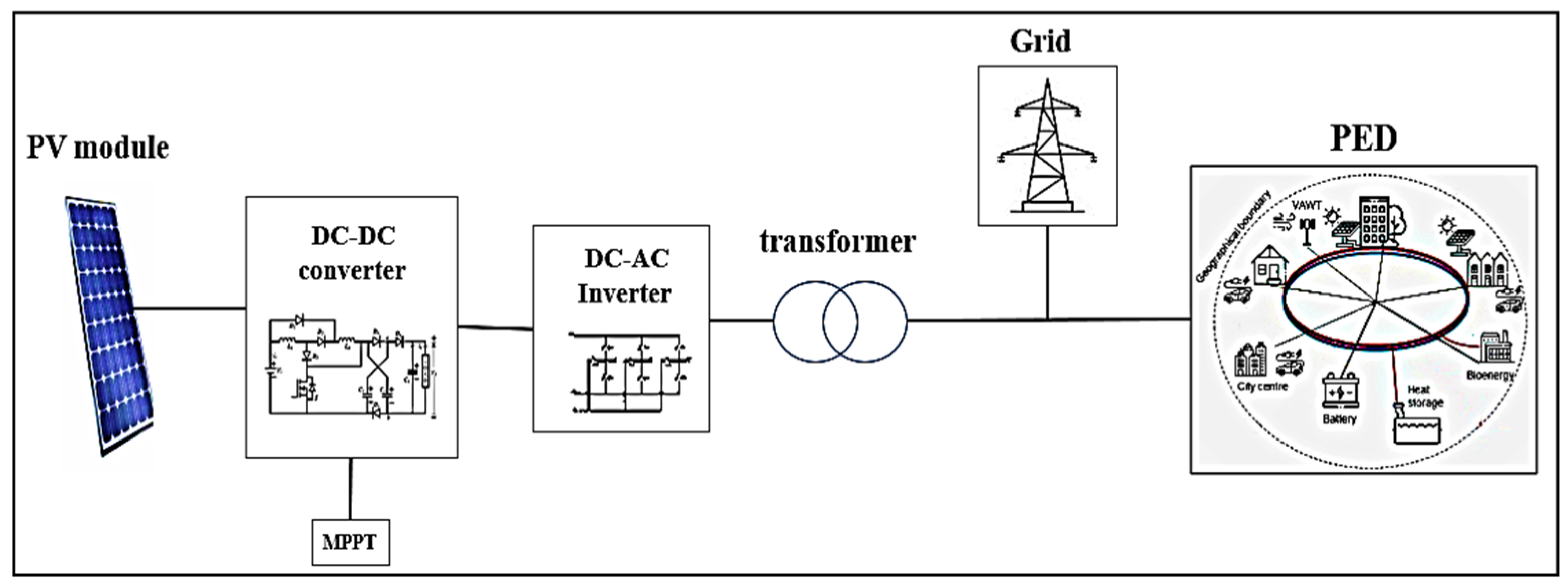
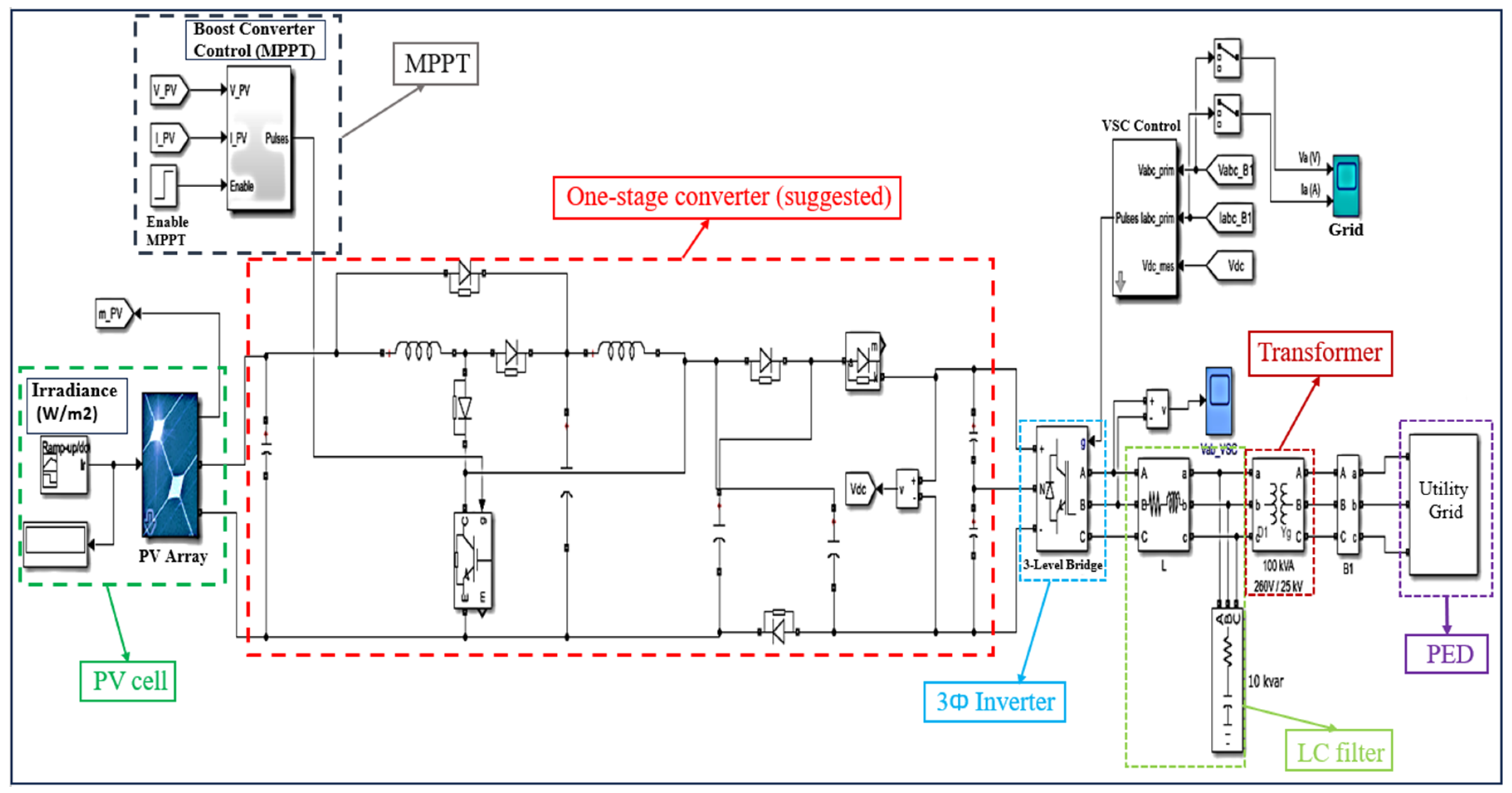
4.2. Grid-Connected PV System for Feeding Electrical Energy into the PED
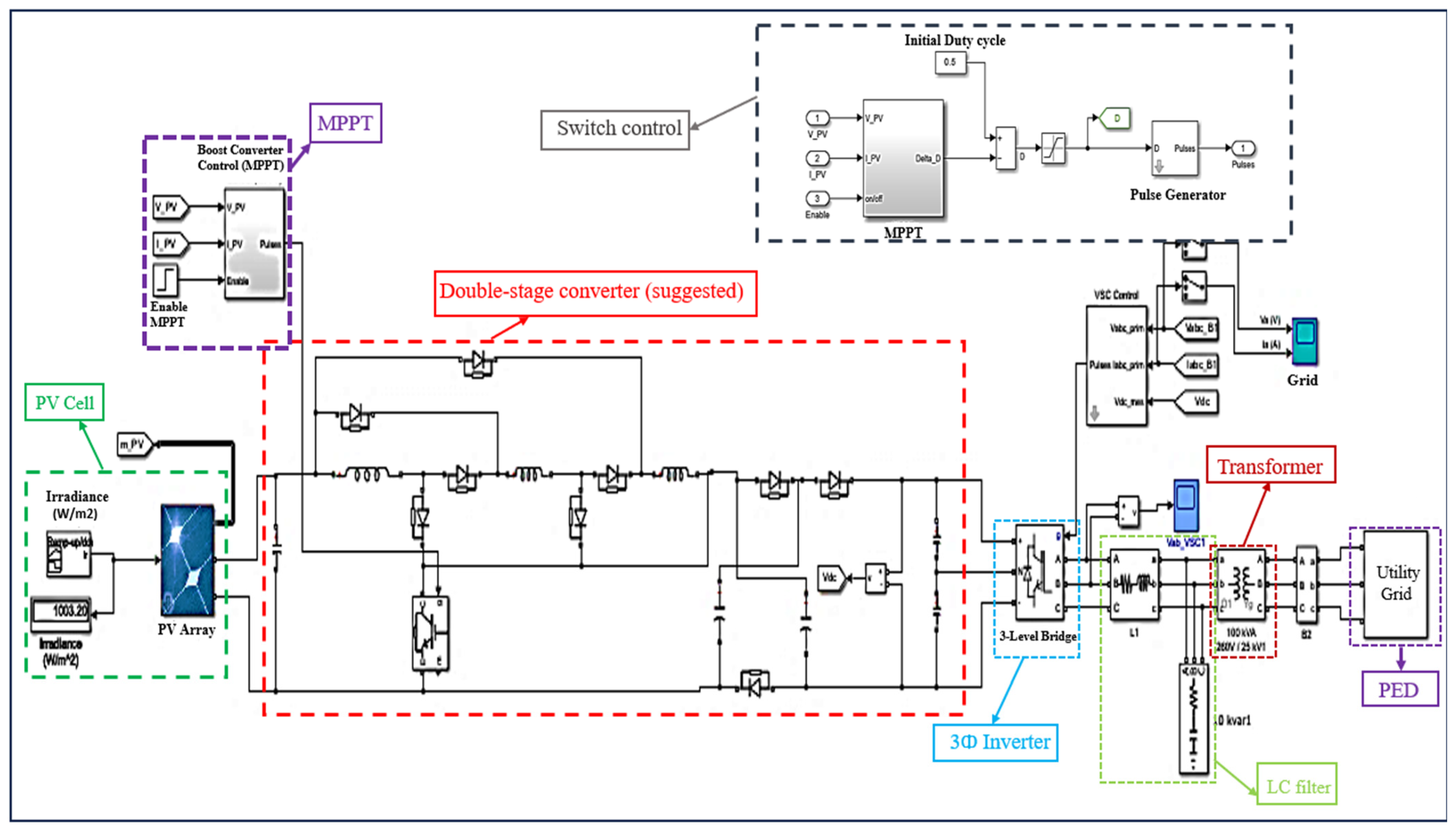
In this paper, a PED-connected PV system was considered. The PV solar array in a grid-connected PV system, sometimes referred to as a “grid-tied” solar system, is “tied” to the local mains’ electricity grid and supplies electrical energy to the PED. The configuration of the solar PV system under study fed to either the PED or the grid, as shown in
Figure 9.
As shown in
Figure 10, the photovoltaic (PV) system connected to the one-stage high step-up DC–DC converter with MPPT, was integrated into a grid-connected system using a 3-level inverter. MPPT is implemented in the DC–DC boost converter by means of a state-flow implementation using the incremental conductance technique as previously demonstrated in [
31,
32].
In the PED-connected PV system under study, 66 strings of five series modules connected in parallel are present, and a high DC–DC step-up boost converter increases the DC voltage from the PV maximum natural voltage, ranging from 273 V to 500 V.
The incremental conductance approach was used to implement MPPT in this DC–DC converter. The MPPT controller changes the switching duty cycle to produce the voltage required for extracting the greatest power.
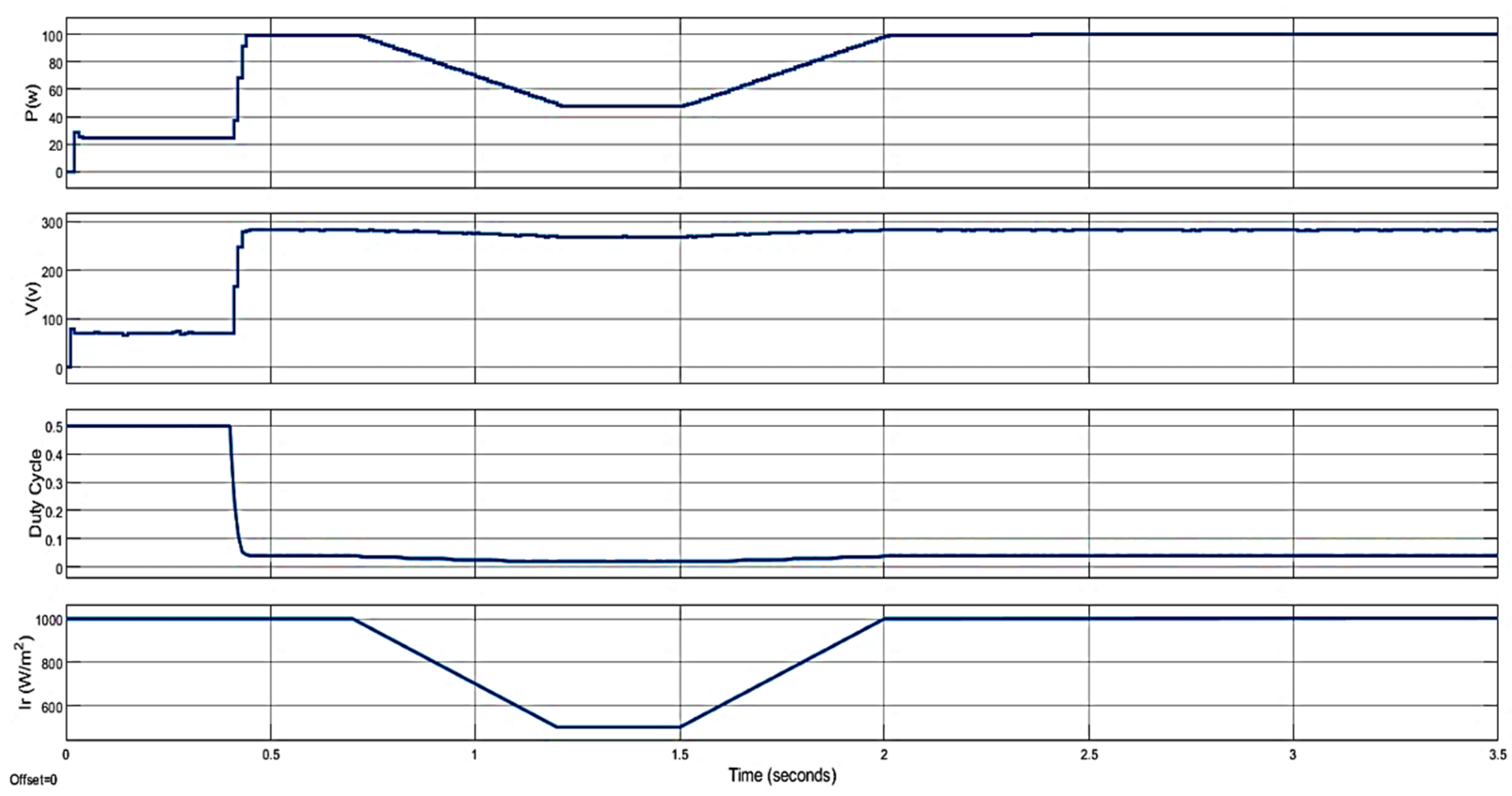
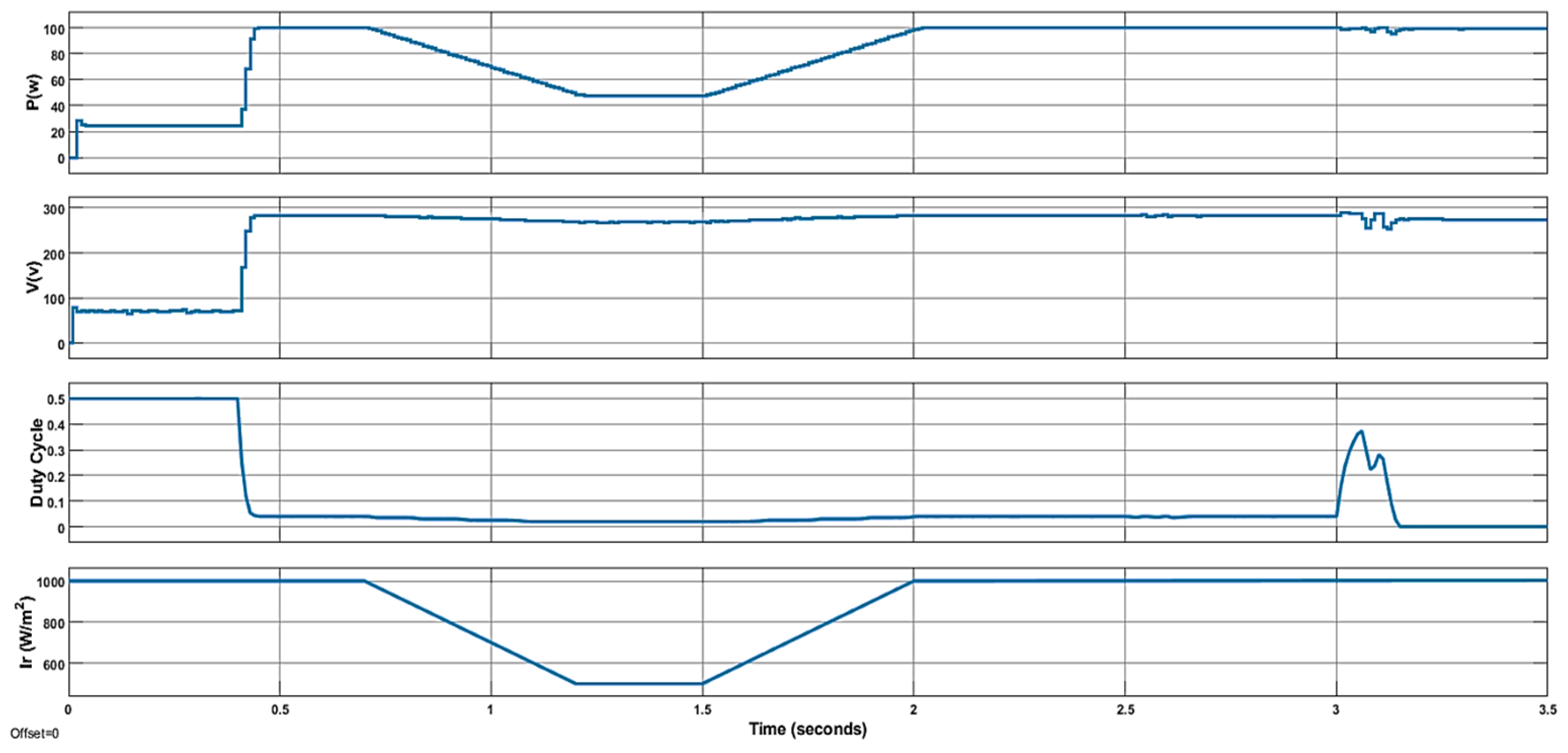
Figure 11 shows the results of a solar radiation experiment conducted to examine the DC side of the system. In this figure, the radiation changed, and in t = 0.4 s, the MPPT is active. As can be seen, the voltage increased to the PV maximum natural voltage of 273 V, and the maximum power according to radiation was extracted.
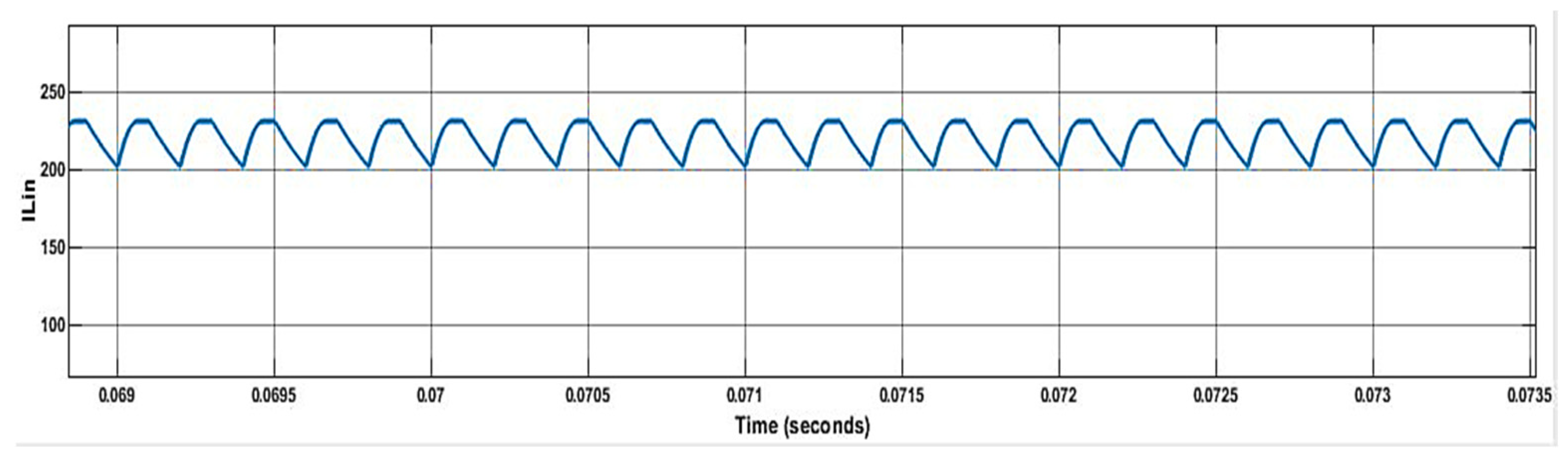
Figure 12 shows the current of the first inductor of the high DC–DC step-up boost converter, and it represents the current flowing through the inductor connected to the converter’s input stage. This current is crucial because it affects the converter’s performance, efficiency, and stability.
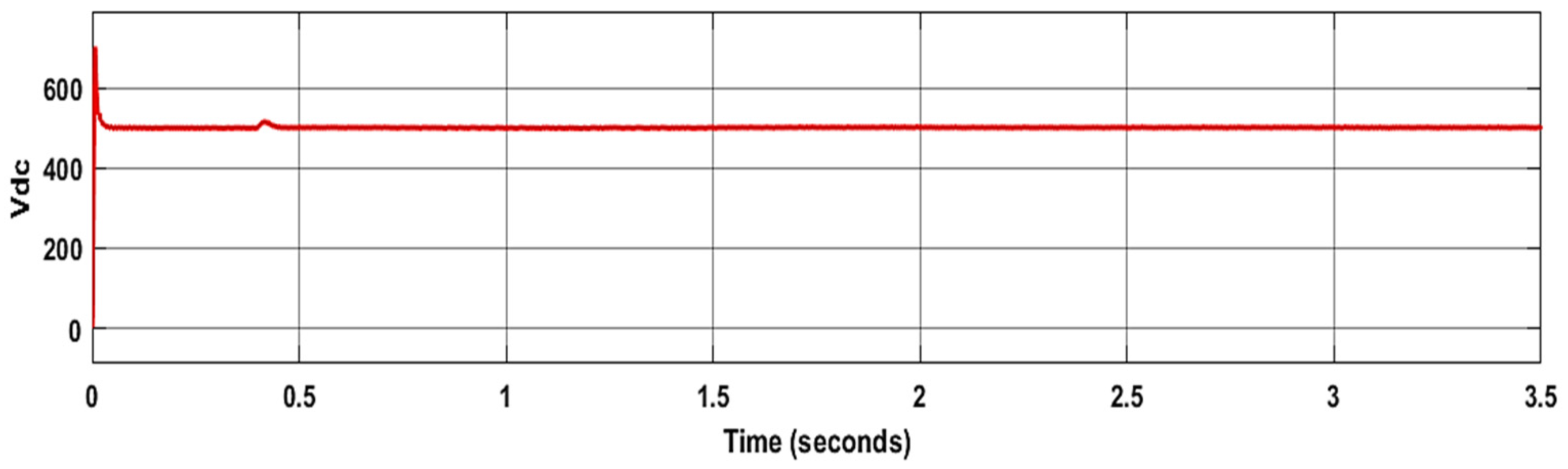
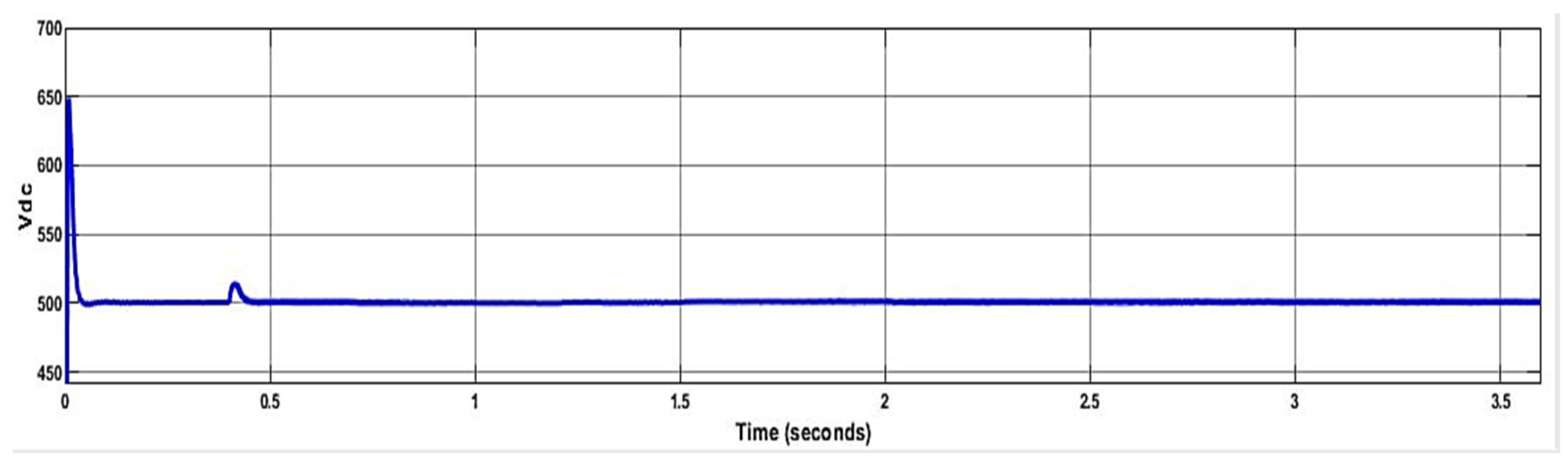
As stated before, the output of the high step-up boost converter was connected to voltage source inverter. The input voltage of the inverter was considered to be 500 v. Consequently, 500 v should be the output voltage of the high DC–DC step-up boost converter. The output voltage of the high DC–DC step-up boost converter is shown in
Figure 13. This figure illustrates the voltage level achieved by the converter after it had increased (or “boosted”) the input voltage.
The voltage source inverter generates alternative current (AC) voltage at 50 Hz. In order to inject this voltage into the grid, a three-phase transformer increases the voltage to a three-phase, line-to-line 25 kV distribution network voltage level.
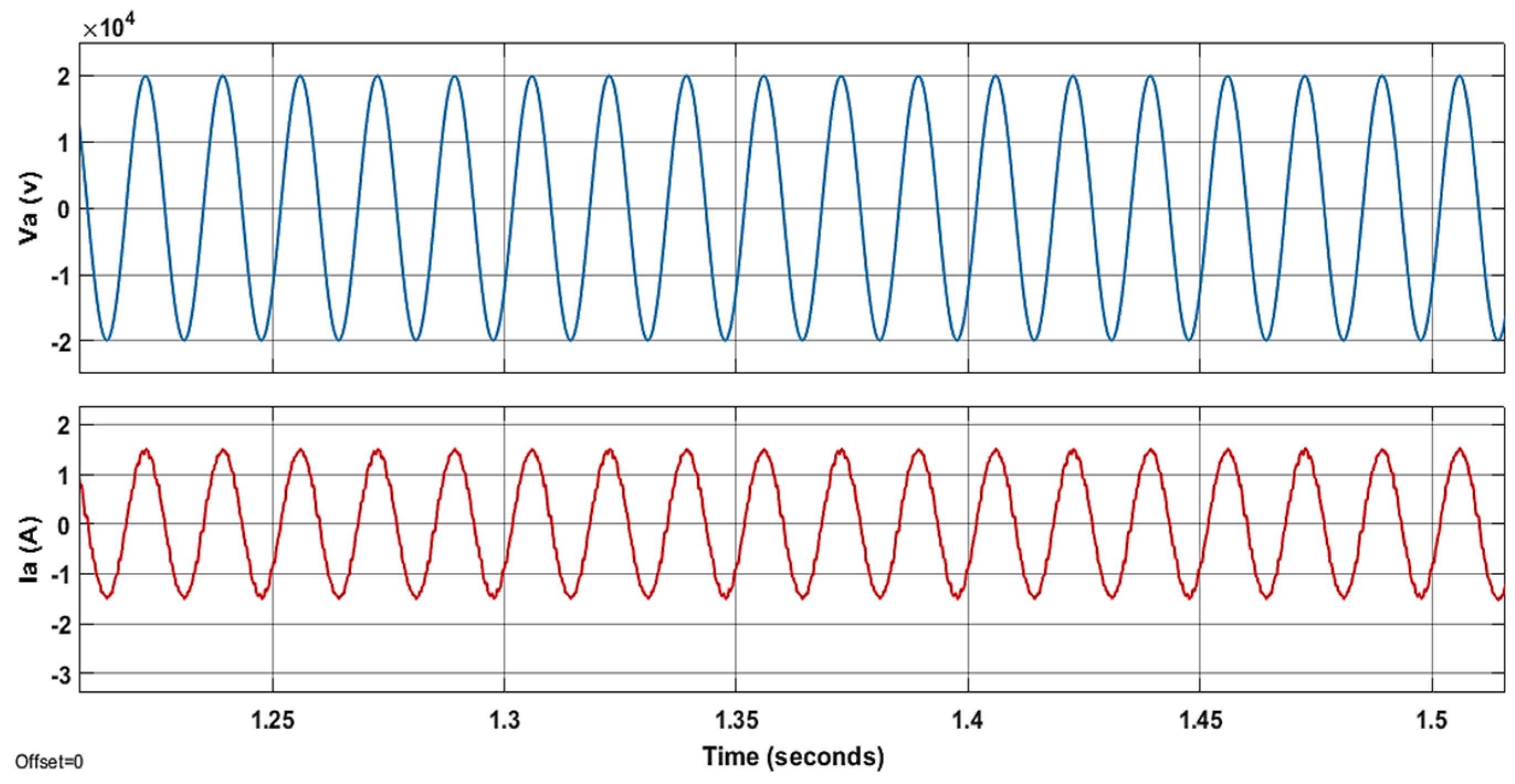
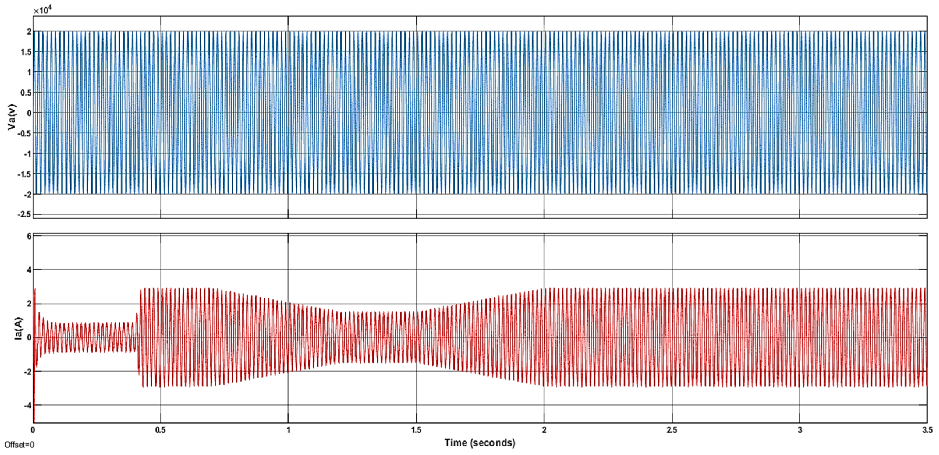
Figure 14 shows the AC output phase voltage and the current of the transformer, and it refers to the electrical parameters produced at the transformer’s secondary winding after it has transferred energy from the primary winding. Understanding these parameters is crucial for evaluating the transformer’s performance and its suitability for various applications.
In
Figure 15, a photovoltaic (PV) system is connected to the double-stage high step-up DC–DC converter that incorporates maximum power point tracking (MPPT). This integrated system is designed to be PED-connected and utilizes a 3-level inverter.
In
Figure 16, the graph displays the current flowing through the first inductor of the high DC–DC step-up boost converter. The results confirm the low input inductor current of converter.
Figure 17 shows the output voltage of the double-stage boost converter and it’s increased voltage level, produced at the converter’s output, which is higher than the input voltage. This output voltage is a key indicator of the converter’s ability to step up voltage to meet specific requirements.
Figure 18 illustrates the AC output phase voltage and the current of the transformer using the double-stage configuration, highlighting their sinusoidal nature. This demonstrates that the proposed approach maintains a low total harmonic distortion (THD) at the point of common coupling (PCC), ensuring compliance with power quality standards. The sinusoidal form of the voltage and current, achieved through advanced modulation techniques and optimized control strategies, minimizes harmonic content, thereby preventing any significant increase in THD at the PCC. This highlights the effectiveness of the double-stage topology in preserving power quality in grid-connected systems.
To analyze the impact of grid disturbances on the PV system, two short-circuit fault scenarios were applied to the one-stage converter.
Scenario 1: A single line-to-ground fault was applied at t = 2.5 s and cleared after 100 ms. During this fault, the system experienced a temporary voltage dip, but the MPPT algorithm quickly adjusted the duty cycle to restore the system’s operating point. This demonstrated the system’s capability to maintain voltage stability and output power recovery despite transient disturbances.
Scenario 2: A three-phase short-circuit fault at t = 3 s, a more severe three-phase short-circuit fault, was introduced and cleared after 100 ms. Despite the significant disruption caused by this fault, the MPPT algorithm effectively re-adjusted the duty cycle, enabling the PV system to return to stable operation. The system maintained output power and voltage stability, underscoring its resilience under more critical fault conditions.
In order to consider the power grid on the PV system, two short circuit faults were applied to the one-stage converter. The first fault type was a single line-to-ground, which was applied at t = 2.5 s and cleared after 100 ms; the second one was at t = 3 s, and a three-phase short circuit fault was introduced and cleared after 100 ms.
Figure 19 illustrates the output characteristics of the PV system under these fault scenarios. The results validate that the proposed configuration ensures operational reliability by maintaining stable performance during faults, highlighting its robustness and fault-tolerant design for real-world applications. This resilience is critical for ensuring the integration of PV systems into power grids with minimal disruption to performance.
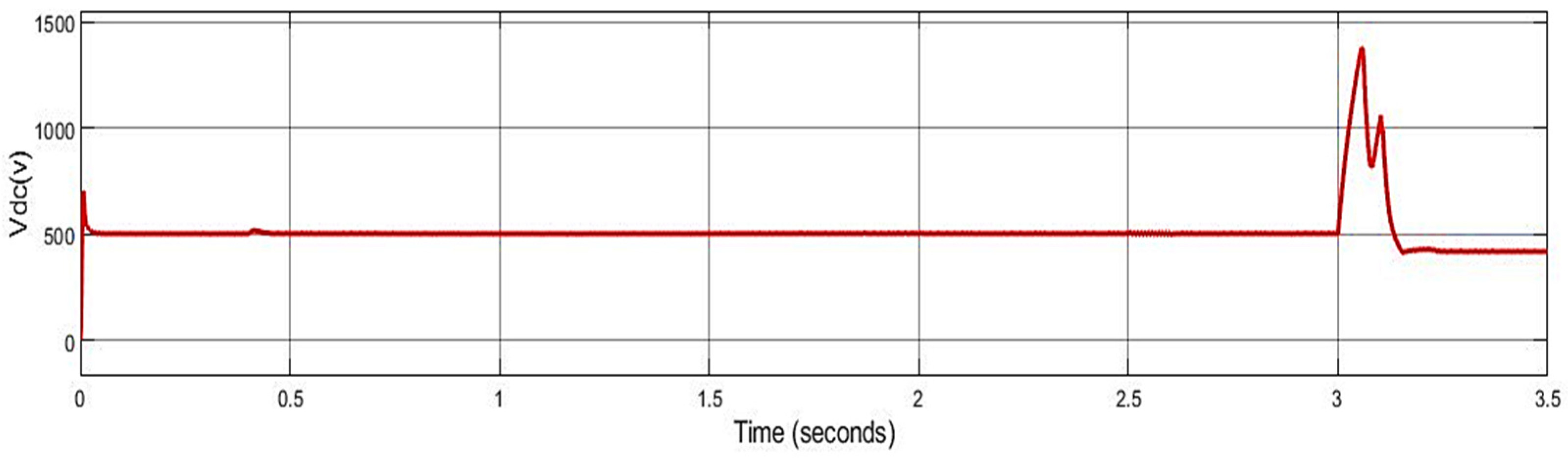
Figure 20 illustrates the DC link voltage under fault conditions, demonstrating the system’s stability even after severe faults. The results show that the DC link voltage remains unaffected during the single line-to-ground fault, maintaining its nominal value without any noticeable deviation. However, during the three-phase short-circuit fault, the DC link voltage temporarily increases due to the abrupt energy imbalance in the system.
This transient rise in voltage highlights the importance of designing the DC link capacitor to withstand higher voltage stresses under contingency scenarios, particularly during severe faults like three-phase short circuits. Ensuring that the capacitor can handle these elevated voltage levels is critical for maintaining the overall reliability and durability of the system under fault conditions.
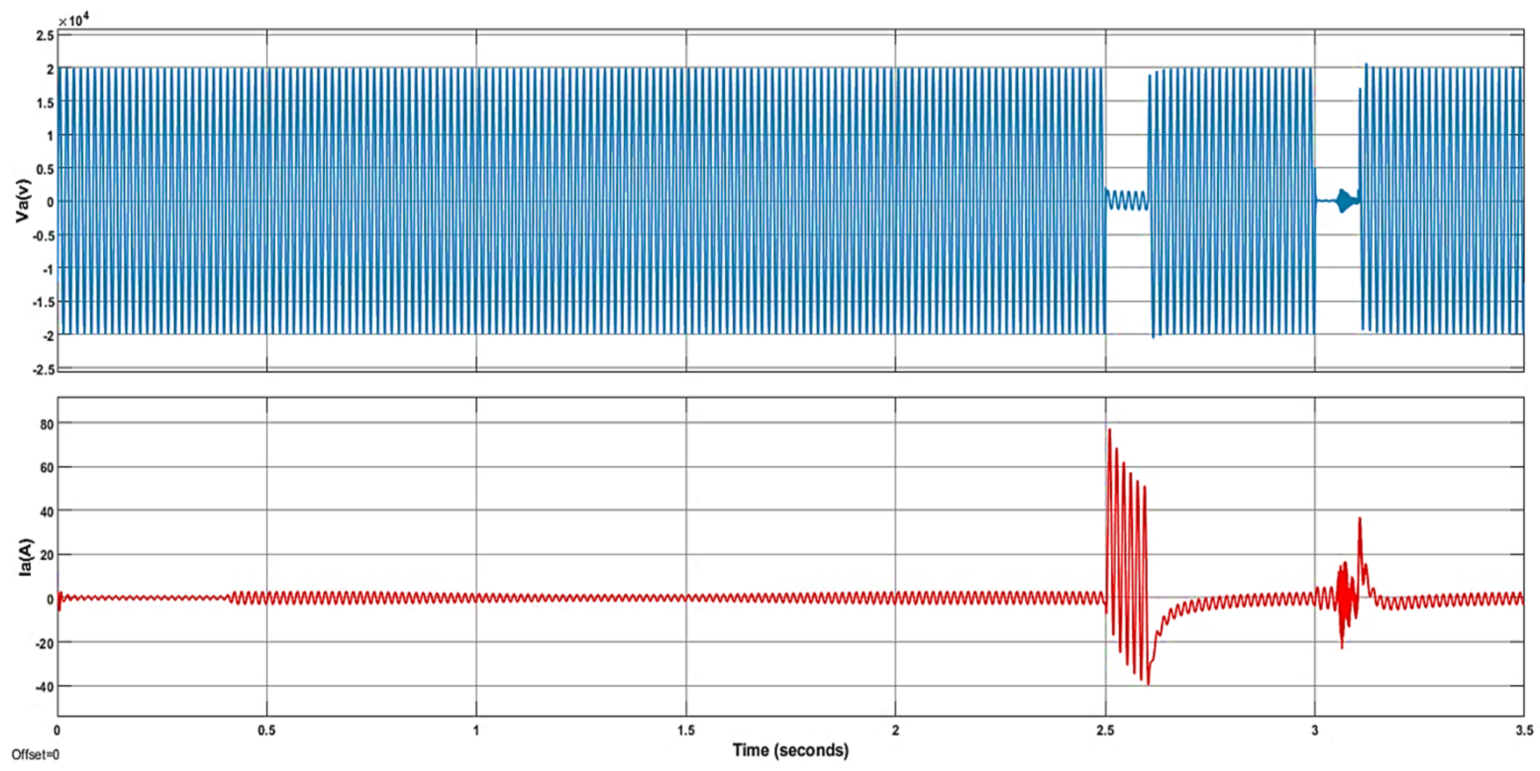
Figure 21 depicts the output voltage and current of the transformer following short-circuit faults. The results show that the output current experiences a sharp spike immediately after the fault, as expected due to the abrupt disturbance. However, the system’s robust control mechanisms quickly mitigate this spike, bringing the current back to its nominal levels within a short duration, thereby preserving system stability.
Similarly, the output voltage exhibits transient fluctuations during the fault, particularly following the short circuit. These fluctuations are effectively damped as the fault is cleared, with the voltage gradually stabilizing to its nominal value. This response highlights the robustness and resilience of the system’s design, demonstrating its capability to handle sudden and severe disruptions while ensuring reliable and stable operations under adverse conditions.
5. Discussion and Comparison
The simulation results presented in this study demonstrate the performance and effectiveness of various non-isolated high step-up DC–DC converters, with a particular focus on their integration into a grid-connected PV system for PEDs. The primary goal was to compare different converter topologies and evaluate their suitability for low-voltage DC sources like solar PV panels in LVDC microgrids. The results offer key insights into the behavior of one-stage and double-stage high step-up converters, as well as their interaction with grid-connected systems under fault conditions. The voltage gain of the one-stage and double-stage converters was calculated as 2(1 + δ)/(1 – δ) and 2(1 + 2δ)/(1 – δ), respectively. For a duty cycle of δ = 0.5, the one-stage converter produced an output voltage of 144 V, with an input of 24 V, and the double-stage converter exhibited a higher gain, delivering even greater output voltages. The performance of these converters under different load conditions suggests that the double-stage configuration provides a significantly higher voltage gain while maintaining a reasonable level of complexity.
The comparative DC voltage gain for different converter topologies, highlights the trade-offs between complexity and performance. While conventional boost converters offer simplicity in design and control, their voltage gain is limited, making them less suitable for high-gain applications in PEDs. On the other hand, the SSIN-based converters, particularly the double-stage configuration, achieve superior voltage gains while keeping the component count and control complexity at a manageable level. This makes the double-stage SSIN converter a strong candidate for applications requiring high-voltage step-up with minimal energy losses, such as in PV systems and battery storage in PEDs.
According to the study, it is evident that while interleaved and zero-switching converters offer high-voltage gains, they come with higher control complexity and an increased number of components. The SSIN-based converters, particularly the one-stage and double-stage configurations, stand out for their balance between topology complexity and voltage gain. The single-switch design in both stages ensures that switching losses are minimized, thereby enhancing overall efficiency. This is especially beneficial in systems like PEDs, where energy efficiency and stability are paramount. The results from the grid-connected PV system simulations with MPPT, further emphasize the robustness and flexibility of the proposed SSIN-based converters. The ability of the one-stage and double-stage converters to maintain voltage stability and system efficiency under varying solar radiation and fault conditions showcases their reliability.
When subjected to line-to-ground and three-phase short-circuit faults, the system remained stable, with minimal impact on PV output power and voltage. The sharp rise in output current after the faults, followed by the rapid stabilization of both voltage and current, underscores the effectiveness of the system’s control mechanisms in managing sudden disruptions. This resilience is crucial for grid-connected systems in PEDs, where an uninterrupted power supply is essential for maintaining the energy balance of the district.
This behavior underscores the efficiency of the SSIN converter’s control mechanisms in maintaining stability during fault conditions, which is essential for systems integrated into Positive Energy Districts (PEDs), where uninterrupted power supply and energy balance are critical. Unlike previous works such as Kumaravel Sundaramoorthy et al. [
21], which focused on the converter’s design and performance under normal conditions, our analysis emphasizes the converter’s ability to handle fault conditions and maintain system stability, a critical factor for real-world grid-connected systems. It should be noted that stability analysis and energy efficiency under fault conditions were not specifically addressed in [
21], whereas our study has provided an in-depth evaluation of these aspects. Our findings indicate that the SSIN converter performs reliably under fault disturbances, making it an excellent candidate for high-efficiency, fault-tolerant applications. This aligns with the need for robust energy systems in PEDs, as highlighted in the literature on fault-tolerant converter designs and their importance for grid stability, such as the studies by Gouveia et al. [
24] and Zhang et al. [
25].
6. Conclusions
This paper addresses the growing need for efficient power conversion in positive energy districts, which rely on the integration of renewable energy sources like photovoltaics, energy storage systems, and smart grids. PEDs require advanced DC–DC converters to manage energy flows efficiently, as renewable sources typically generate energy in DC form. High-performance DC–DC converters ensure minimal energy losses during conversion, optimizing the district’s overall energy production and consumption. In this context, the development of novel converter topologies is essential to maximize energy efficiency and system reliability.
Novel one-stage and double-stage SSIN converters are proposed, with the DC voltage gain of the suggested converters derived analytically. The gain was determined to be 2(1 + δ)/(1 − δ) for the one-stage converter and 2(1 + 2δ)/(1 − δ) for the double-stage converter. An innovative approach was adopted by modifying the one-stage and double-stage methodologies to simulate a PV power system. This system integrates maximum power point tracking within a grid-connected system using a 3-level inverter. The incremental conductance method was employed in the state flow implementation of MPPT in the DC–DC boost converter. To evaluate the PV system’s interaction with the power grid, two short-circuit faults were applied. The results indicate that, following both line-to-ground and three-phase faults, the current increases; however, the system remains stable even under severe fault conditions. Furthermore, the use of a single semiconductor switch in the SSIN topology, regardless of the number of stages, was found to enhance the converter’s overall efficiency. This makes it an excellent candidate for integrating low-voltage DC sources, such as batteries and fuel cells, particularly in applications like PEDs. The converter can also be adapted for use with other inverter types, such as the S3 inverter.


