1. Introduction
In recent years, there has been strong renewed interest in hydrogen production technologies and fuel cells for powering electric propulsion systems. The interest in hydrogen is all the greater in those contexts where high autonomy is required, and the exclusive use of battery packs as power sources introduces strong volume and weight issues. One such context is undoubtedly the maritime transport sector, where all-electric ships are garnering increasing interest [
1].
The Argonauts team of the University of Bologna-UniBoAT is a research project involving students and researchers that moves, with these considerations, toward expanding the knowledge about the use of sustainable propulsion systems in the context of mobility.
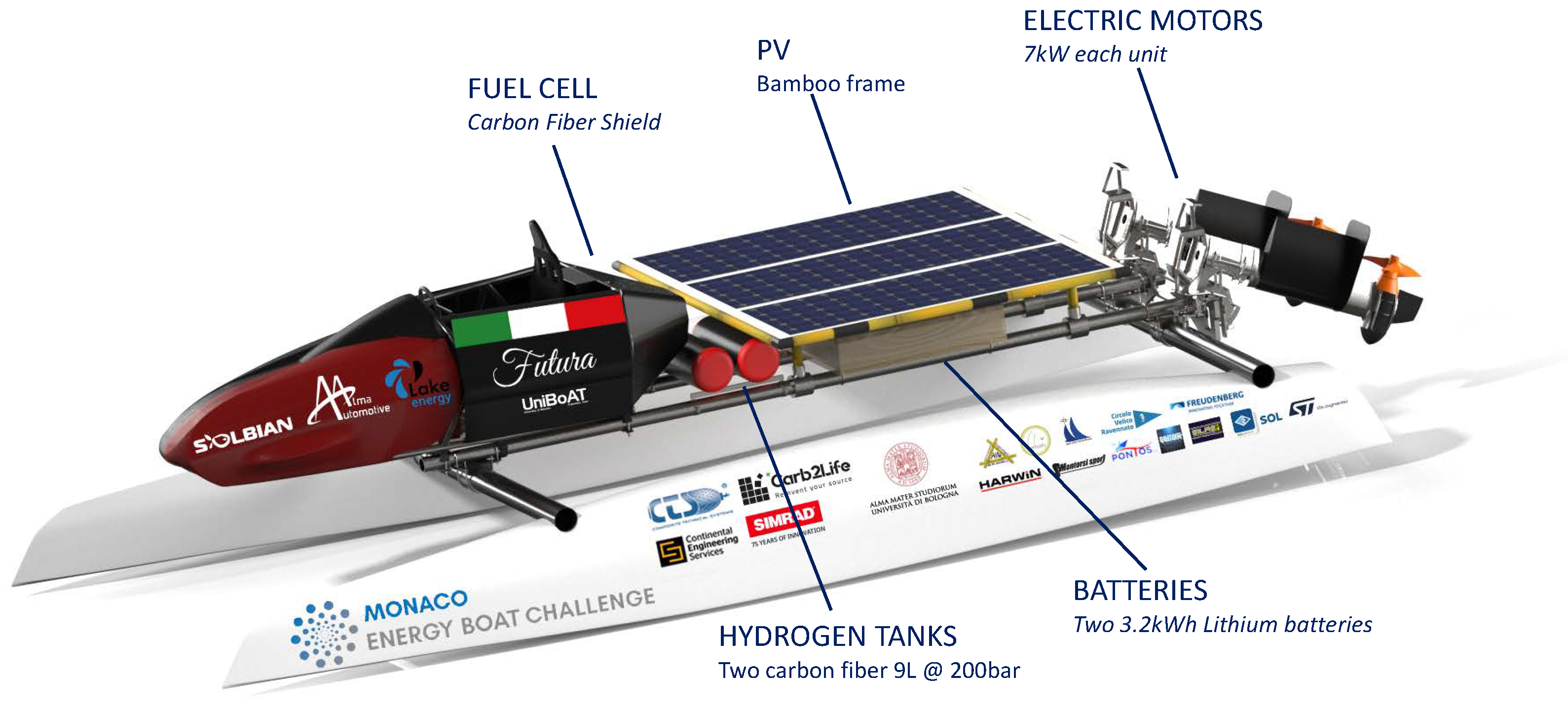
In recent times, the UniBoAT team developed Futura, a racing catamaran prototype powered by CO2-free energy sources supplying an outboard electric motor. The Futura’s propulsion system is based on a mix of currently available sustainable technologies: high-efficiency photovoltaic panels, a self-built Li-Ion battery and a high-pressure hydrogen tank supplying a proton-exchange membrane fuel cell (PEMFC).
In July 2021, the Argonauts team participated for the first time in the “Monaco Energy Boat Challenge 2021”, an event hosted by Yacht Club de Monaco [
2]. The boat developed by the team competed in the Energy class, which consists of designing the chassis and the propulsion system to be installed on the catamaran hulls. The hulls were provided by the organization, and they were the same for all participants of the class. The Monaco Energy Boat Challenge includes four challenges: an endurance race of 3 h, a slalom track, a speed record and a one-by-one elimination race. The Monaco Energy Boat Challenge rules for the endurance race stipulate a maximum on-board stored energy of
and a maximum boat weight, without a pilot, of
. In the 2021 prototype, the energy was managed 60% by a battery and 40% by a fuel cell. The fuel cell was operating through its own OEM controller and a DC-DC converter with a total weight of
(excluding stack weight). Details of the Futura catamaran are visible in
Figure 1.
This work moves from this first architecture with the aim of improving the converter stage within the development of the new 2022 Futura prototype. The main idea behind the new concept was to obtain a completely novel design, making the fuel cell and converter assembly a single, integrated, stand-alone device based on automotive-grade components. This process, while starting from well-established practices regarding the structure and control of converters, required original solutions in both mechanical integration and design issues for power converters.
One of the most sensitive aspects of the project relates to the peculiar operation of fuel cells. Although FCs demonstrate good output power capability during steady-state operation, the dynamic response during transients, especially at peak power demand, is relatively slow [
3]. This is why FCs are often combined with energy storage systems such as batteries or supercapacitors to improve the capabilities of supplying energy during fast power transient and to recover energy during regenerative breaking [
4]. Therefore, a DC/DC boost converter is essential to match the FCs’ low operating voltage with the generally higher voltage of the lithium battery packs [
5]. In the studied application, and for other applications for electric propulsion, the DC/DC converter has to meet several requirements. They are here briefly summarized:
Several DC/DC boost converter topologies have been documented in the literature [
7,
8]. Their advantages and disadvantages are effectively summarized and compared in [
9,
10].
Standard boost converter topology, despite being extensively used in renewable energy applications [
11], is not able to meet all the mentioned requirements. This is because the use of massive inductors and capacitors is necessary to keep the current ripple at the required low level [
12].
Isolated resonant LLC converters are valid alternatives, especially in such applications with high-voltage levels where galvanic insulation between FC and battery is required [
13,
14]. Resonant DC/DC converters provide higher voltage gain and allow one to increase the conversion efficiency by using soft-switching techniques [
15]. However, LLC converters require more complex control and the use of additional components, such as the compensation capacitors and the (often custom-made) transformer. Eventually, the efficiency of these converters is greatly variable with changes in the working point. This makes this architecture not optimal for a wide operating range, especially in the case of a light load [
16].
Multi-phase interleaved boost converters (IBC) are promising candidates. This topology family consists of several standard boost stages (phases) connected in parallel and independently controlled [
17,
18,
19]. The interleaving technique, i.e., the control of the different phases with different relative phase shifts, is the most preferred way for parallelizing because it allows obtaining relevant reductions in input current ripple and output voltage ripple while increasing their frequency, together with low switching loss and a usually faster transient response [
12,
17,
20]. Despite this architecture requiring an increase in the number of inductors (one for each phase), an increase in the ripple frequency allows a strong reduction in their size [
21,
22]. Moreover, the efficiency of interleaved converters can be kept high across the whole operating range by adopting phase shedding [
23]. It is for these reasons that this topology was the one adopted in the application that is the subject of this paper.
This work thus starts by choosing architectures and methods validated in the literature and describes their adaptation to create a novel conversion stage. In particular, we intend to present all those design choices that allowed us to integrate the DC/DC converter directly into the metal frame containing the FC stack, eliminating the use of a dedicated heat sink without altering the structure and performance of the FC. As better described in the dedicated
Section 2, this converter was also developed to operate in a manner compatible with the short circuit unit. The IBC here proposed has been designed to work at a high switching frequency of
in order to reduce as much as possible the inductors’ size and weight. This choice has a great impact on PCB design and the selection of the components. The design of the electronic boards and traces and ground-plane placing are fundamental to ensuring low switching losses and limiting electromagnetic emissions. Some unconventional choices in PCB design are also discussed. The converter and the whole system of FC+converter have been tested in both laboratory and real conditions.
The remainder of the paper is organized as follows.
Section 2 provides the description of the application.
Section 3 and
Section 4 discuss the design of the multi-phase interleaved converter and its firmware, respectively. The simulation results and experimental validation details are provided in
Section 5 and
Section 6. Finally, the conclusions are presented in
Section 7.
2. Description of the Application
Along with other technologies that make use of renewable sources, fuel cells (FC) are gaining much attention as practical solutions to respond to the environmental issues related to vehicular propulsion. PEMFC is the most promising FC technology because of its higher efficiency, low operating temperature and pressure and easy maintenance [
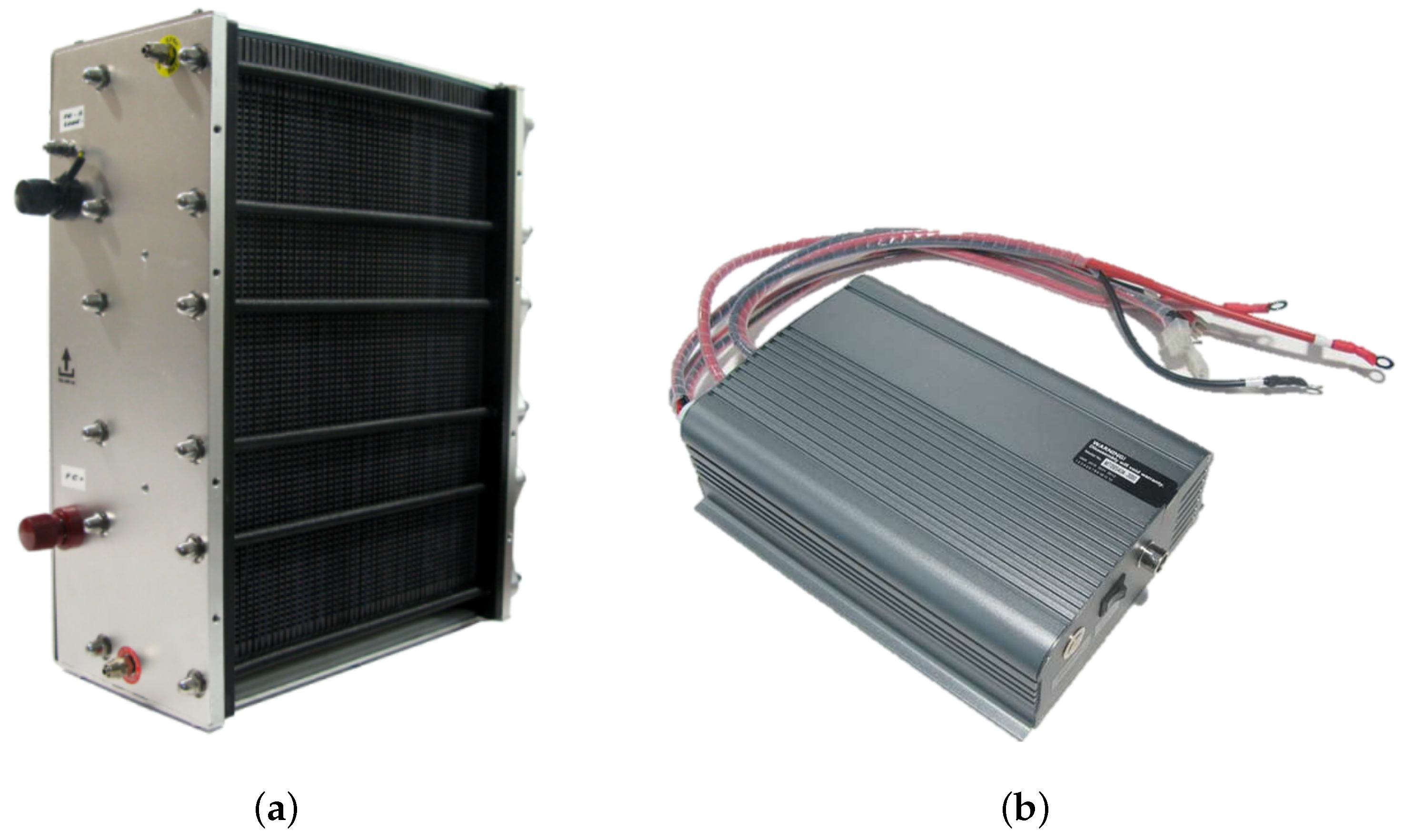
24]. The application referred to in this work has been developed around the air-cooled PEMFC Horizon H-2000 shown in
Figure 2. This fuel cell has a rated power of
for a size of
and a weight of
. This FC is originally sold together with its OEM controller (
Figure 2b) weighing
and without any power converter device.
The FC is composed of a stack of 48 PEMFCs which are enclosed in an aluminum frame that supports and protects them. The two fans visible on the front side are devoted to airflow circulation with the aims of providing oxygen for the FC reaction and cooling down the device.
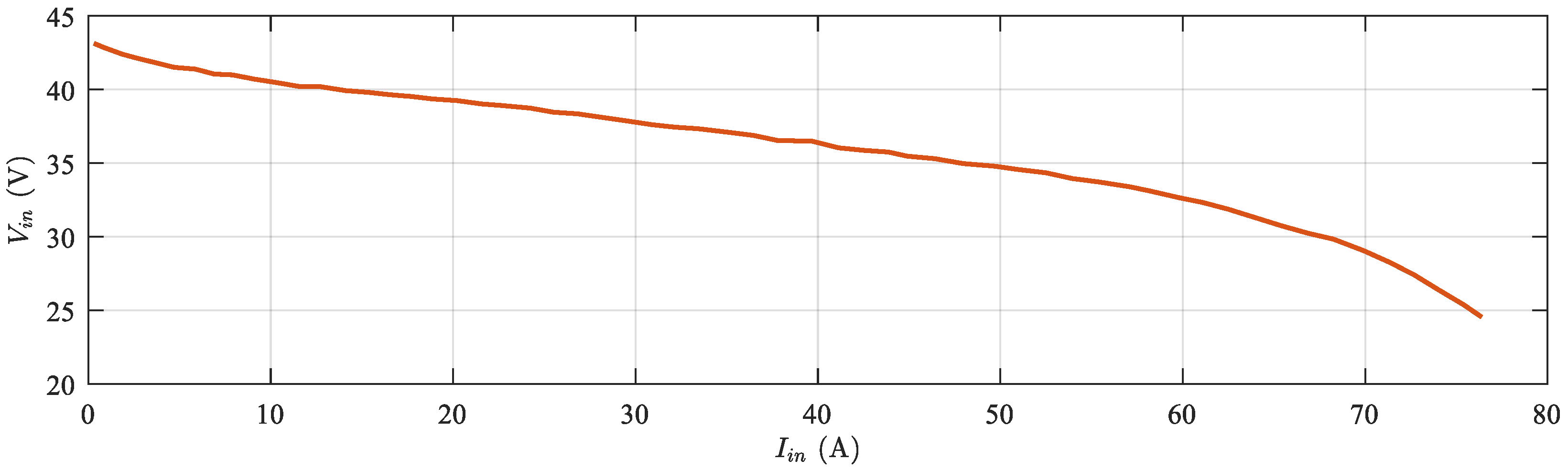
Each cell of the stack has an open circuit voltage of
, resulting in a no-load voltage of about
. The electrical behavior of the whole stack is shown in
Figure 3.
The most critical issue owing to PEMFC is that its efficiency is greatly influenced by its operating point. For this reason, its output current must be accurately regulated by means of a dedicated power converter [
26]. The regulation provided by the DC-DC converter is fundamental also because the PEMFCs’ output voltage varies based on the condition of its stack’s temperature and hydrogen pressure [
27].
It is worth mentioning that the adopted PEMFC is equipped with the so-called short circuit unit (SCU). The SCU is a device that short-circuits the PEMFC output terminals for an interval of
every
[
28]. As indicated by different scientific works [
29], this short circuiting procedure improves the performance of the stack over time, aiding also the moistening of the proton exchange membranes of the cells.
For the FC output regulation, many works, specifically those in the automotive field, proposed topologies such as the buck-boost converter, the interleaved boost converter, and other isolated DC-DC converters [
30,
31]. Among these architectures, the DC-DC boost converter is the one that presents high efficiency, together with a reduced component count [
9,
32]. According to this, the present work considers a synchronous interleaved boost converter (SIBC) specifically designed to work with the PEMFC and a contemporary acting as a charger for a Li-ion battery pack [
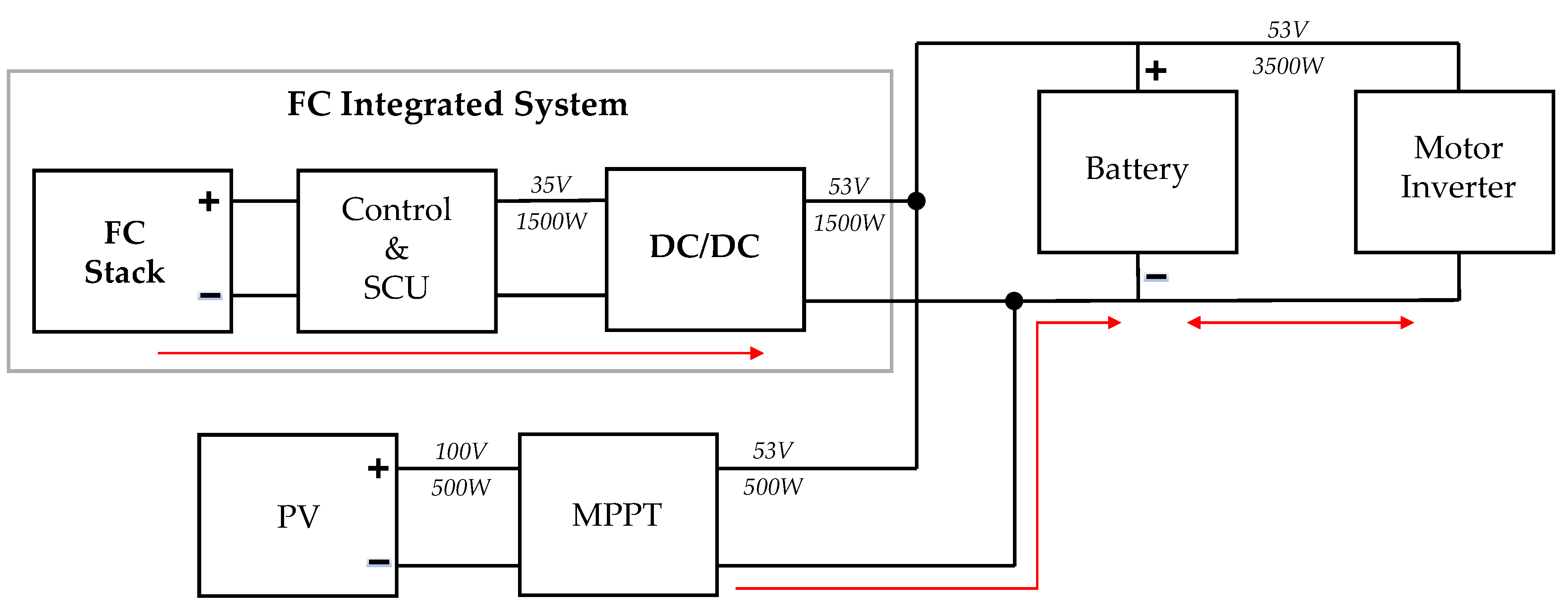
20]. The coupling with the battery is necessary because the principle of operation on which the fuel cell is based does not allow it to operate under conditions where high dynamics are required unless its performance is compromised. In the application under consideration, the power demands during the competition would instead require sudden power variations. Therefore, the battery is used to supply the rapid variations and power peaks that the fuel cell alone would not be able to handle [
33]. The resulting traction chain scheme and the related energy flow diagram are reported in
Figure 4.
Along the whole traction chain of the catamaran, the voltage level is limited to a threshold value of . This choice allowed us to increase the safety level, avoiding at the same time the use of isolated power converter topologies, providing a strong benefit in terms of overall weight reduction.
As the converter has been specifically designed for sports competition, its design had as its key targets the maximization of efficiency, the highest possible weight reduction and mandatory high reliability. The adopted PEMFC offered approximately
efficiency when working in a power generation range lower than (
). According to the required accuracy in the regulation of output voltage and currents, the power electronic converter is controlled through the average current mode control (ACMC) technique. This control technique in fact, by directly regulating the average current flowing in the inductor, ensures enhanced accuracy in the input current control [
34]. Other common switching-mode power supply (SMPS) control strategies, e.g., peak-current mode, suffer from poor noise immunity, a need for slope compensation, and most of the possible peak-to-average current errors [
35,
36].
3. Design of the Converter
This section discusses the SIBC’s hardware (HW) and firmware (FW) design choices. The basic technical requirements for the design of the converter are reported in
Table 1.
As mentioned in
Section 2, the design of the converter started from the fundamental requirements of reliability under the goals of weight minimization and efficiency maximization. Among the different possible architectures of the converter, the interleaved boost topology has been considered the most suitable one. This topology has numerous features that make it particularly suitable for the application under consideration. The interleaved structure allowed the current to be distributed over multiple switches, reducing both conduction and switching losses. By acting on the control of the different interleaved legs so as to operate them with appropriate phase shifting, it is possible to reduce the ripple amplitude of the output current and increase its effective frequency, thereby reducing the current operated by each switch, making it possible to choose components with a lower current value and allowing higher switching frequencies. All this results in a strong reduction in all filter elements, i.e., inductors and capacitors, resulting in strong reductions of weights. Furthermore, the reduction of the ripples in input current and voltage has been proved to significantly improve the PEMFC lifetime, hence increasing the reliability of the whole power conversion stage [
6,
37,
38,
39].
The interleaved architecture also meets the need for reliability by strongly improving the fault tolerance of the converter. In fact, even if one of the switches fails, the remaining phases can continue to operate by accepting a derating of the current [
40].
Finally, the interleaved configuration opens up the possibility to perform phase shedding at the low-load level to improve converter efficiency [
23].
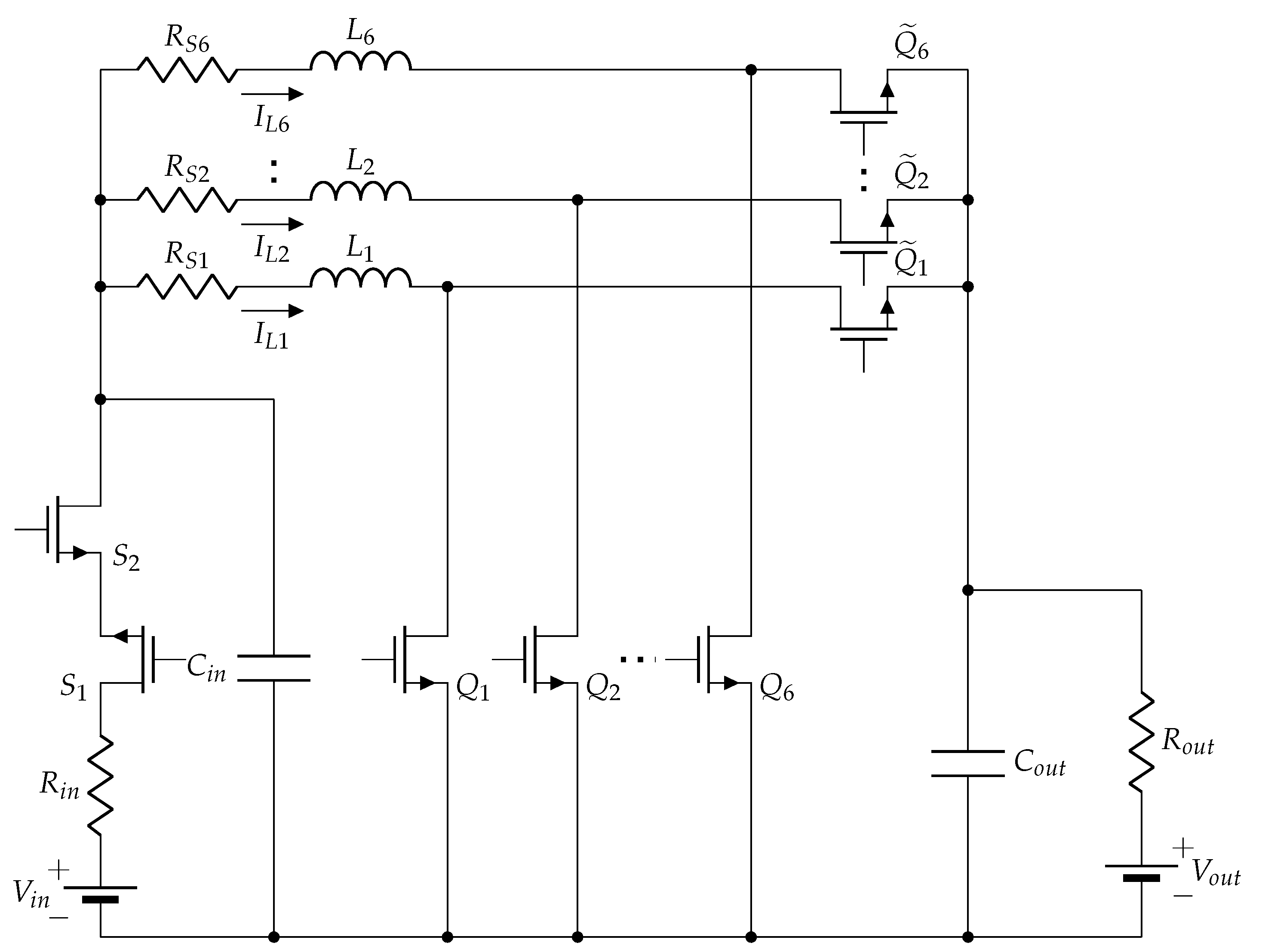
3.1. Converter Architecture
Following a comparative evaluation that considered the usable space constraints; voltage and current levels; and possible micro-controllers that could be employed to implement the converter control, the architecture shown in
Figure 5 was adopted.
Hence, the implemented converter resulted in six interleaved legs in the SIBC. The two mosfets, and , connected in the so-called back-to-back configuration, are operated as electronic relays to guarantee the possibility of decoupling the source and the load voltages to prevent the circulation of currents through the body diodes of the top side mosfets . This decoupling action is also essential to prevent the discharge of the SIBC’s input bus capacitors during the PEMFC short-circuiting, allowing one to disconnect the PEMFC output from the converter’s input side in case of occurrences of system faults. Hence, these mosfets have been selected with the lowest possible drain-to-source on-state resistance with the aim of reducing the conduction losses. In fact, these switches are mainly operated in static conditions, for which the dynamic performances assume secondary importance. The actual SIBC is based purely on mosfets avoiding diodes. This is again with the aim of taking advantage of the lower conduction resistance that these devices present with respect to diodes. According to the adopted six-leg architecture, the control of each leg is phase-shifted of , and each mosfet has to conduct only of the whole current managed by the whole converter. The adopted mosfets can be operated at a switching frequency of . Therefore, the output current ripple will present a frequency six times higher. This has allowed us to reduce the size of the filter inductors on each leg and the size of the electrolytic capacitor .
The resistors
are shunt resistors that have been chosen as current sensing devices thanks to their simplicity, extremely reduced power losses and good performances offered with respect to other current sensing devices [
41].
3.2. Inductor Design
The sizing of the inductors has moved from the evaluation of the expected duty cycle operating range through Equations (
1)–(
3) that refer to minimum, maximum and nominal duty cycles, respectively, [
18,
42].
The value of the inductor is put in correlation with the duty cycle and the input voltage through Equation (
4) by imposing the maximum allowed ripple current
:
where
T is the switching period.
The minimum value of the inductance is evaluated through Equation (
5) with respect to the nominal average inductor current
. For the sake of simplicity, the maximum allowed inductor ripple current
has been set as equal to 60% of
.
The obtained value needs an additional assessment with the minimum value of inductance that guarantees that the converter will operate in continuous conduction mode (CCM) for values of the input current higher than .
This is particularly important because synchronous switching is possible only if CCM is guaranteed (this aspect is detailed in
Section 4.3).
is evaluated as:
The actual value of the adopted inductor is related to the most stringent constraint value among
and
, i.e., the one able to guarantee the respect of both conditions [
43]. The values obtained in the design phase are reported in
Table 2.
3.3. Other Components of the Power Stage
In this specific application, the choice of the output bus capacitors is not critical because of the adopted interleaved architecture and the contemporary direct connection to the battery pack that helps to smooth the output voltage. However, a electrolytic capacitor was still inserted to filter out some of the harmonic content of the residual ripple. Conversely, the choice of the proper input capacitance was carried out with the help of circuit simulation to guarantee the respect of the desired ripple specifications while verifying compliance with the physical space limits.
The evaluation led to the choice of a solution based on the parallel connection of six
multi-layer ceramic capacitors (MLLCs) and one
electrolytic SMD capacitor for each phase. These hybrid solutions based on two different technologies allowed us to realize efficient filtering on the whole harmonic spectrum of the current ripple [
44]. The power mosfets were selected from the Infineon Technologies AG SMD bottom-cooled portfolio [
45] to achieve a reasonable balance between expected conduction losses (i.e., low on resistance) and switching losses (i.e., low gate capacitance). In each phase, a fast, dual-channel mosfet gate-driver was used [
46]. This device provides input-to-output isolation, protecting the MCU, and thanks to a high-output current rating, it is able to drive the mosfet at a high switching frequency. The high-side mosfet gate-to-source voltage is obtained by means of bootstrap circuitry consisting of a
ceramic capacitor and a Schottky diode. Chosen components are listed in
Table 3.
The datasheet values of the selected components were put in the circuit simulation model built in the LTspice (by Analog Devices Inc., Wilmington, MA, USA) environment to assess the power stage performance. Additional details are provided in
Section 5.
3.4. PCB
Downstream of the selection of the components and the verification of the main converter performances through circuit simulation, the design of the PCB followed. Its manufacturing specifications are summarized in
Table 4.
The thickness of the copper layer was chosen to ensure the proper current density ratings. Sizing was done using Saturn PCB Design Toolkit [
49]. The PCB was designed while making reference to the FR4 dielectric material and taking the input power supply line as a reference with the most stressed trace. As the FR-4 material presents a high-glass transition temperature
, the maximum working temperature was assumed to equal
. In addition, due to the quite high switching frequency and the relevant number of analog signal traces on the board, a four-layer PCB was chosen as a suitable layout able to provide appropriate shielding to possible electromagnetic interferences (EMI) [
50].
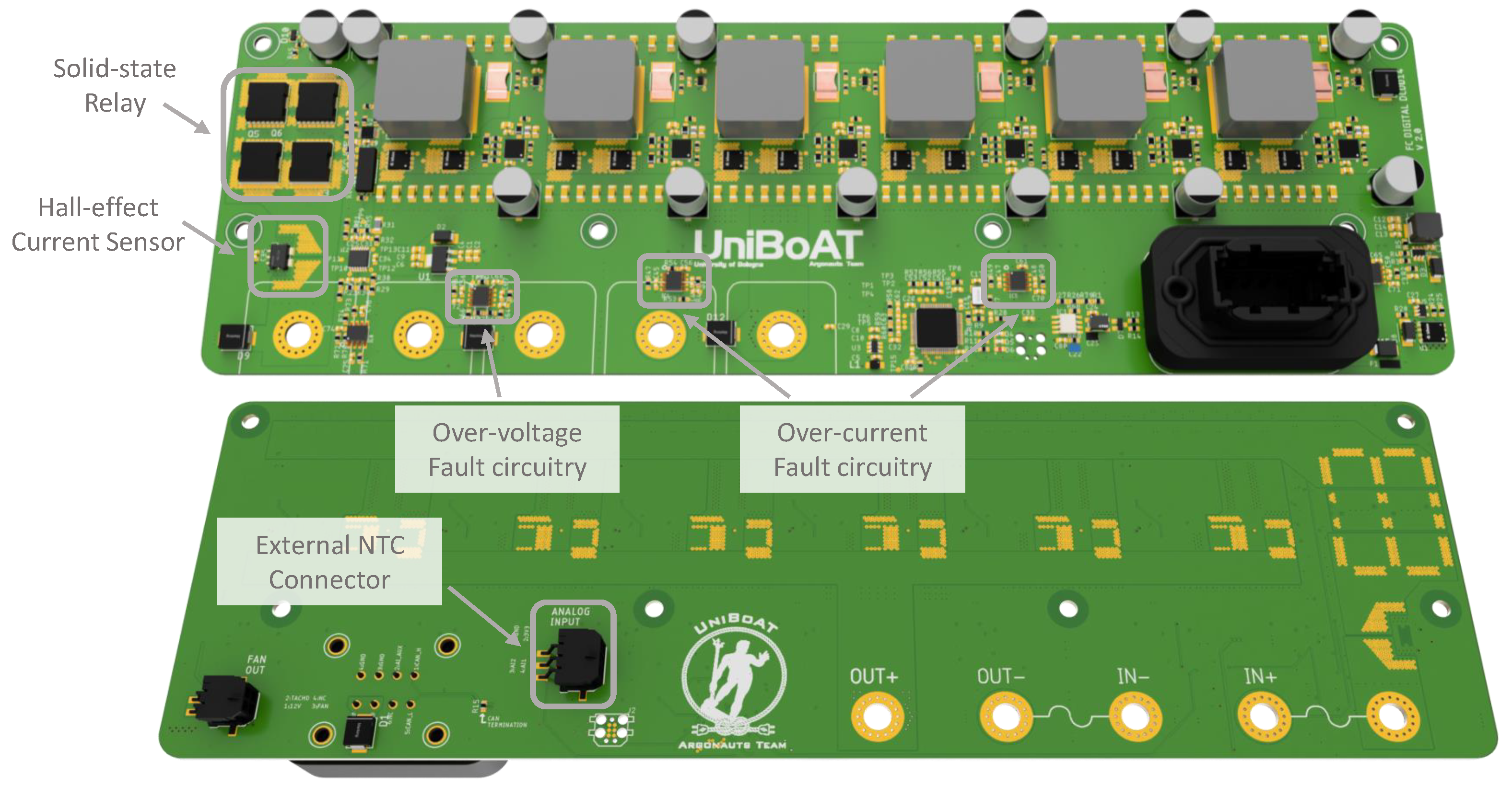
Figure 6 shows the obtained PCB with the second-phase components concealed to make visible the circuits underneath. These parts are also detailed through the magnification on the left side.
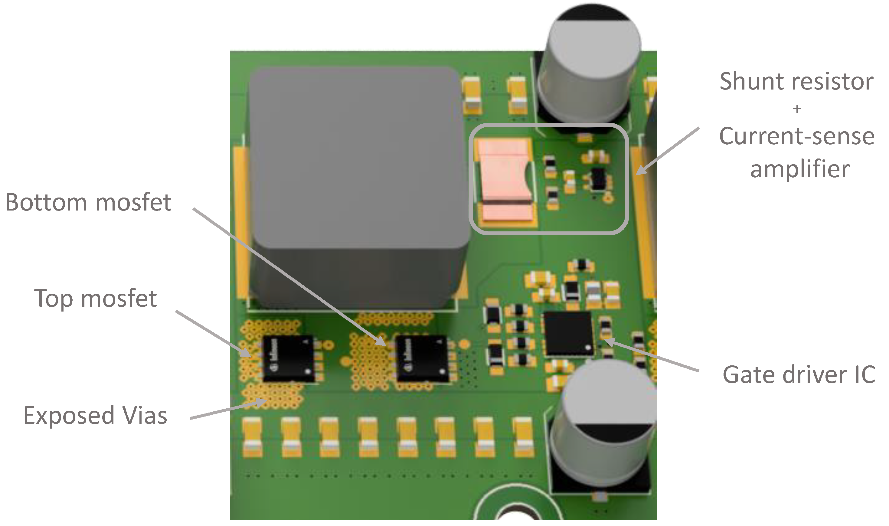
For what concerns the placement of the components, particular effort was made to minimize the commutation loop of the mosfets. According to the high operation frequency adopted for the switches, the reduction of these loops is essential for the reduction of parasitic inductances resulting from the circuit traces that could introduce intolerable oscillations and overshoots during mosfet transitions [
51]. In order to minimize the number of components adopted with a view to increasing the reliability of the converter, capacitors were not inserted near the rheophores of the mosfets, but the reduction in the switching loop area was obtained by building the loop traces vertically from top to bottom, utilizing inner layers. This allowed to restrict the loop area to the only PCB core thickness [
50].
The bottom side of the PCB was kept empty to aid the heat transfer towards the PEMFC aluminum frame. In fact, in order to push weight reduction as far as possible, no specific heat sink was provided for the converter, but the external structure of the fuel cell was exploited instead. The thermal interface was further improved through a thermal gap pad and by placing
vias close to most stressed power components (make reference to
Figure 7 magnification).
3.5. Safety and Fault Protection
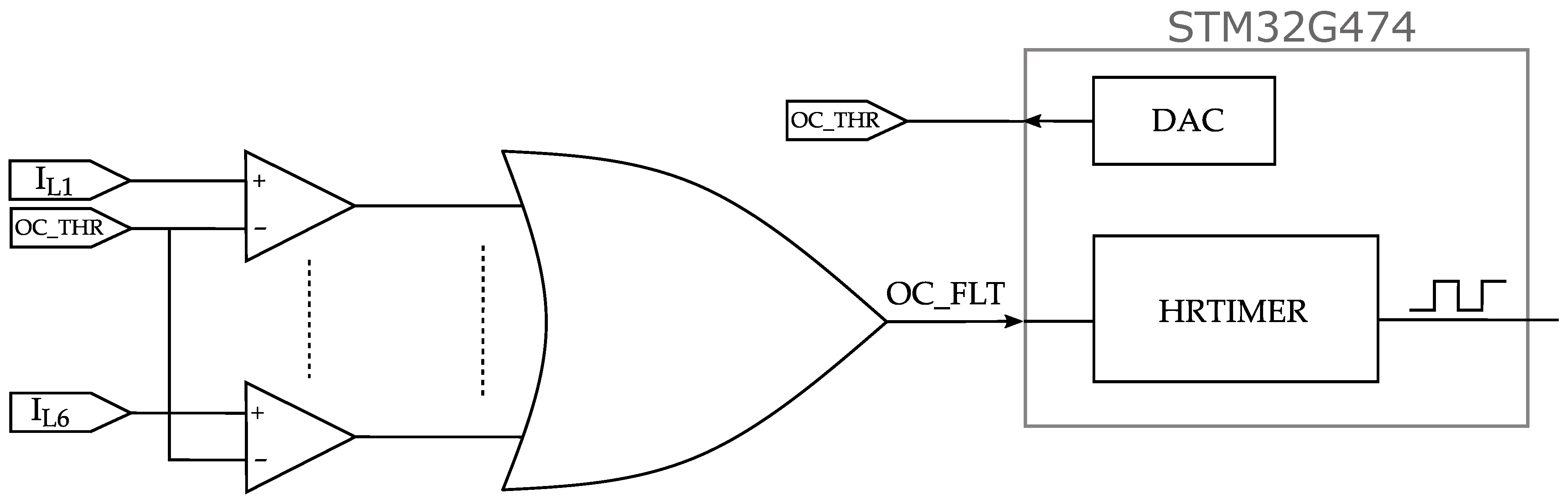
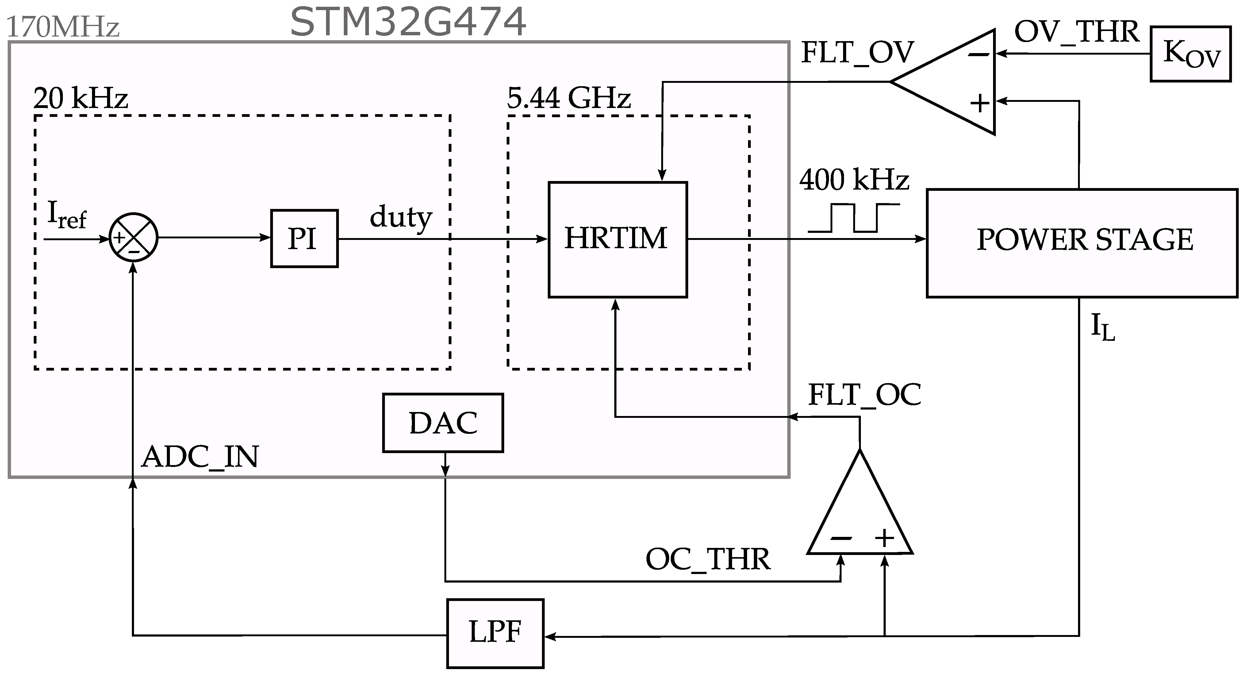
Safety was taken into account during the design phase. Despite the conventional peak-current mode control scheme, where the overcurrent can be easily identified and reduced on a cycle-by-cycle basis, this approach is not possible under ACMC due to the high switching frequency [
52]. However, thanks to the advanced features of the adopted microcontroller that provide dedicated fault input lines, all gate drive signals are immediately turned off once the fault condition is detected. In this way, low latency fault protections can be implemented.
The two substantial faults considered during the design phase were:
Inductor overcurrent: Turn off the power stage if any of the inductor currents reach the fault threshold. This avoids a mosfet fault caused by controller errors and at the same time protects from output short-circuits. The threshold is made software-configurable via a CAN bus and must be 8–10 A higher than the average phase current taking the ripple into account.
Input and output overvoltage: Turn off the power stage as soon as input or output voltages exceed a critical threshold level. This allows one to safeguard the electrolytic capacitors and prevents battery overvoltage.
The comparable logical network for overcurrent fault prevention is shown in
Figure 8. The current measured at the shunt resistor is amplified and fed directly into each phase’s open-drain operational amplifier (Op-Amp). Using the Op-Amp, each stage is configured to compare the signal to a voltage generated by a digital to analog converter (DAC). Then, the output of all the comparators is linked to form an OR gate, which is further connected to a high-resolution timer (HRTIMER) that generates the switching signals. Overvoltage protection uses a similar concept, except that the threshold is determined by a voltage divider; thus, it is fixed on the HW side to
and
. Finally, hardware protection against overcurrents is provided by means of fuses installed on both the input and output stages in the points indicated by the fuse symbol on the bottom side silk screen in
Figure 6.
4. Firmware Design
SIBCs require precise digital control, which needs the use of a microcontroller unit (MCU) featured with specific peripherals. The STM32G474 MCU by STMicroelectronics was chosen because this MCU is designed to address specific digital power conversion applications, such as Digital Switched-Mode Power Supply (D-SMPS) and motor-inverters.
The STM32G474 MCU has dedicated peripherals called HRTIMER that can achieve
resolution and generate complementary six-pair PWM output signals using a delay-locked loop (DLL). In addition, a dead-time generation unit is added to govern the signal’s rising and falling edge without the need for a specific software implementation. The main computation unit is an Arm
® 32-bit Cortex
®-M4 CPU with a floating-point unit (FPU) operating at
, ensuring adequate calculation performance to handle the controller loops and CAN communication interfaces [
53].
4.1. Architecture
The firmware architecture is distinguished into two levels. One level is devoted to the soft-periodic functionalities, such as the external communication interface and the main finite state machine (FSM). These can be implemented on a real-time operating system, i.e., FreeRTOS developed for STM32 MCUs. A second level of the firmware manages the so-called hard-periodic functionalities, i.e., current control loops and duty cycle synchronous updates. These hard-period functionalities are executed inside the time-driven interrupt services routines.
Figure 9 depicts one of the six parallel boost phases’ control logic. A proportional-integral (PI) controller is used to regulate the current. The amplified signal taken from the shunt resistors is used to implement overcurrent protection before being averaged by a low-pass filter (made by a simple RC network) and monitored by the analog to digital converter (ADC) integrated into the MCU. The microcontroller keeps the control loop at
and writes the updated duty cycle set-point to the HRTIMER control register.
4.2. PWM Signal Generation
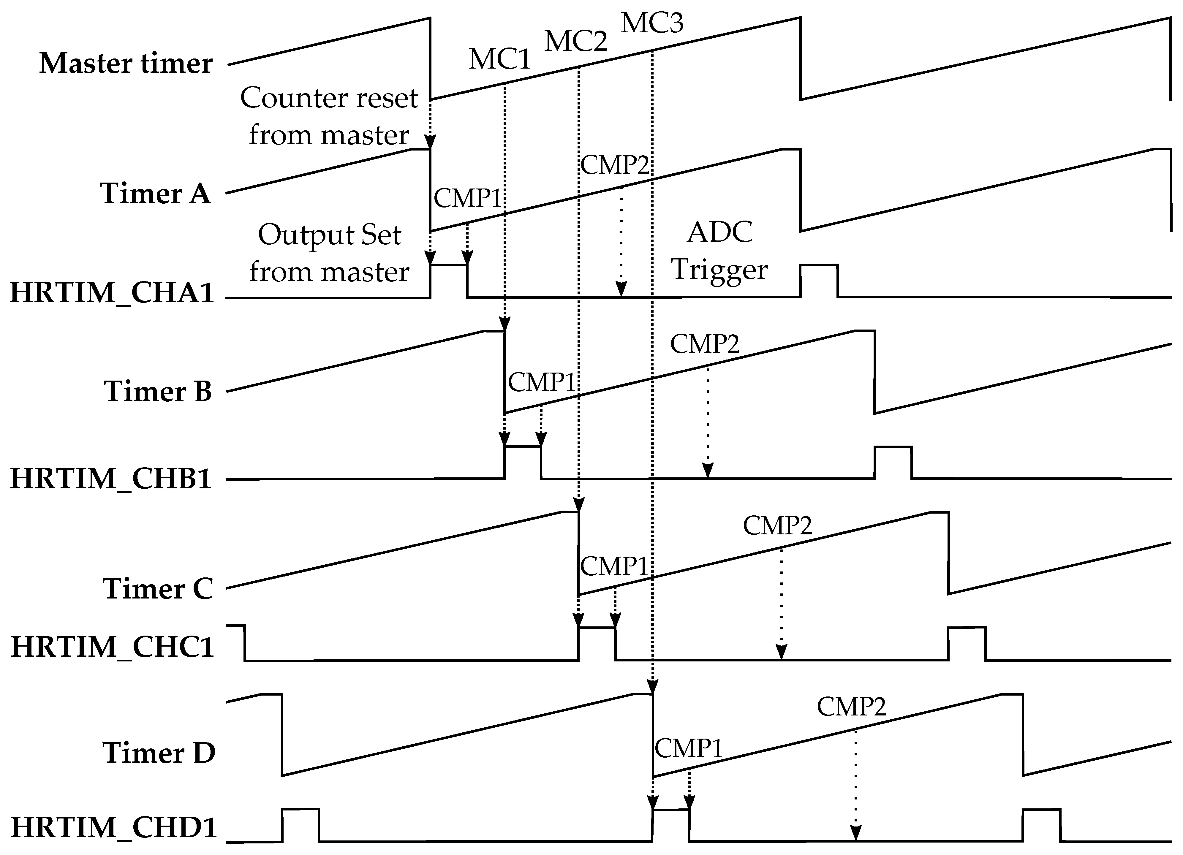
The generation and updating of PWM signals are some of the most critical and challenging tasks for the management of the interleaved architecture. In fact, the parallel nature of the selected topology necessitates accurate duty cycle synchronization.
Among the specialized peripherals integrated into the MCU, the HRTIMER was designed specifically for this purpose. It comprises seven counting units, including a master and six slave timers, each of them with two output lines. For each timer unit, there are also four comparators. The master timer oversees phase management: while regularly resetting the slave clocks, it establishes a phase connection between the different legs of the boost converter. The relative phase shift is calculated by dividing
by the number of phases, which is maintained at
in this application. The master timer is set to continuous mode; thus, it counts the switching period roll-back till zero and starts again. The slave timers, instead, are set to re-triggerable single-shot mode and wait for master timer comparator events before start counting after their period is reached. The duty is imposed separately from the phase shift into each of the timers. This allows for phase shedding, which helps modify the number of active phases in real-time depending on the operating conditions (especially for light load [
23]).
What has just been described is detailed graphically in
Figure 10.
Analog conversions are initiated by a slave timer’s second comparator, which is set to create a trigger at half the switching-off time. The ADC channel corresponding to the proper current signal is sampled when the event occurs. Switching disturbances are minimized as much as is feasible by selecting the sample point [
54].
4.3. Reverse Current Control
Another fundamental aspect that needs to be considered while controlling a synchronous DC-DC converter connected to a battery is the occurrence and management of the DCM operation condition. In fact, when the inductor current falls to zero, the battery starts to supply current toward the input through the high-side mosfet, which is, at this time, conducting. DCM operation occurs under a light load, i.e., when the average inductor current is lower in comparison to the ripple. This phenomenon can be disruptive for the converter and cause degradation of the FC; therefore, it must be avoided. The easiest solution is to adopt the classical non-synchronous boost topology which intrinsically prevents negative current flow by replacing top side mosfet with a diode, but it has the drawback of efficiency loss (2–3%).
The solution implemented here follows the mode boundary detector approach presented in [
55]. This method identifies the two operating conditions on the basis of the parameter
k, defined in Equation (
7).
The converter operates in CCM for all values of ; conversely, it operates in DCM for . At every control loop iteration, according to the k sign, the topside mosfet is kept off in case of DCM or enabled for CCM. A safe margin is also added, and non-synchronous mode is kept at every set point change and during the start-up phase.
5. Simulation Results
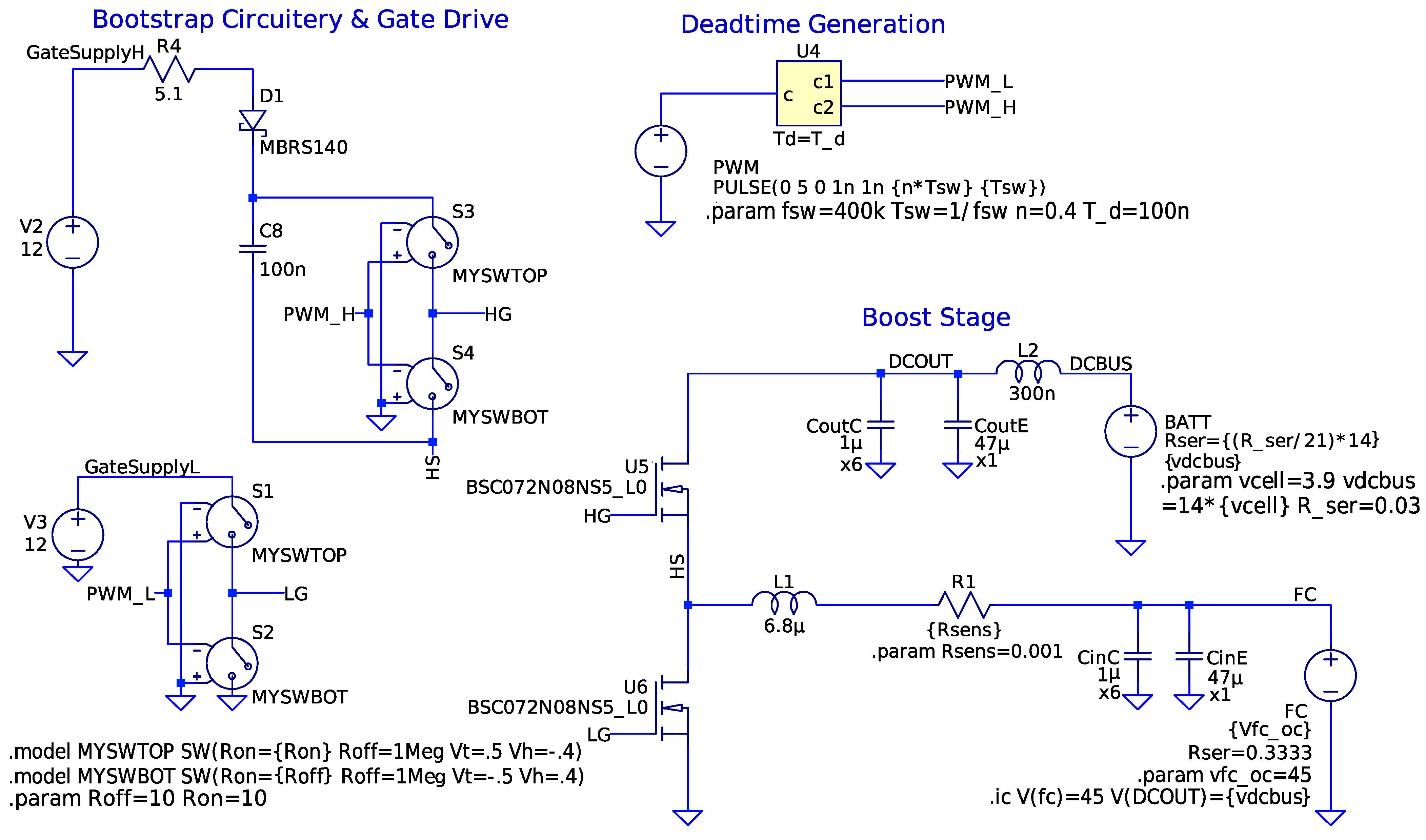
As introduced in
Section 3.3, the validation of the design was performed by simulating the main components of the power stage on LTSpice.
Infineon Technologies AG provides the SPICE model for the selected device, allowing for a quite accurate simulation of its dynamic behavior [
56]. The circuit model of one phase of the power stage is shown in
Figure 11. It includes three circuit blocks: dead-time generation logic, gate drive, and bootstrap circuitry; and one phase of the synchronous boost converter. Battery and FC are simply modeled as non-ideal voltage sources with series resistance to approximate their dynamics under load. The adopted value of the battery ESR was obtained by starting from the available information referred to the single cell ESR and considering their parallel–series arrangement inside the whole battery pack. The fuel cell ESR was extracted as a first-order approximation of the voltage–current characteristic curve reported in
Figure 3.
Several simulations under different working conditions have been carried out to verify that the power components were working within tolerable voltage and current ranges and to validate the expected efficiency of the whole converter. The maximum values of critical electrical quantities for the main components of the power circuit have been given in
Table 5. These values, extracted from the respective datasheets, are compared with the maximum values obtained in the simulation.
It appears clear that all the components are working well below their maximum rated limits. Indeed, an adequate safety margin was taken in order to to ensure the highest possible reliability by considering simulation uncertainties and accounting for possible variability due to variation in ambient working temperature.
Table 5 reports also the information related to the bootstrap diode used for the powering of the high mosfet drive.
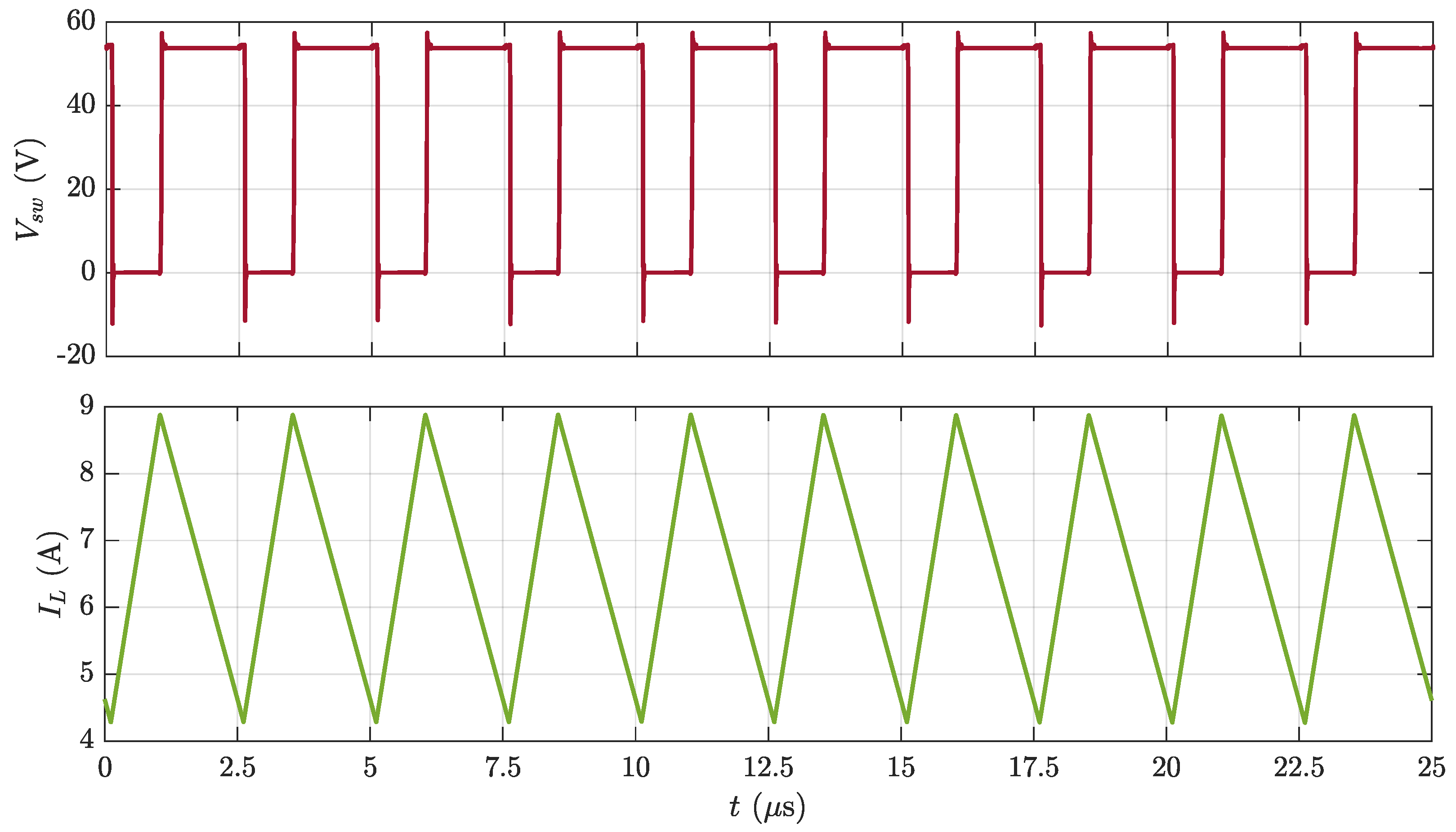
Finally, the whole six-phase power stage was simulated to assess the complete design with respect to the initial input–output ripple requirements.
Figure 12 shows the waveform of the switching node voltage and the inductor current while the converter is operating at nominal conditions (i.e.,
,
and
).
Even if the inductor current ripple related to each phase presents a relatively high value of
, the combination of the input capacitor and the operation of the six-phase interleaved arrangement has to lead to a low-input-current oscillation with amplitude slightly lower than
. The resulting input current ripple shown in
Figure 13 results in
of
, satisfying the converter’s requirement.
The obtained power conversion efficiency was within the range when the converter worked in synchronous mode and under non-synchronous-mode operation.
6. Experimental Validation
This section presents the results regarding the tests carried out on the prototype built on the basis of the evaluations and analyses presented in the previous sections. The results presented refer to both the tests carried out in the laboratory and those carried out in the real field.
6.1. Bench Test
The laboratory tests were carried out by using a bench power supply and an electronic active load to validate the converter functionalities and its performances in safe conditions.
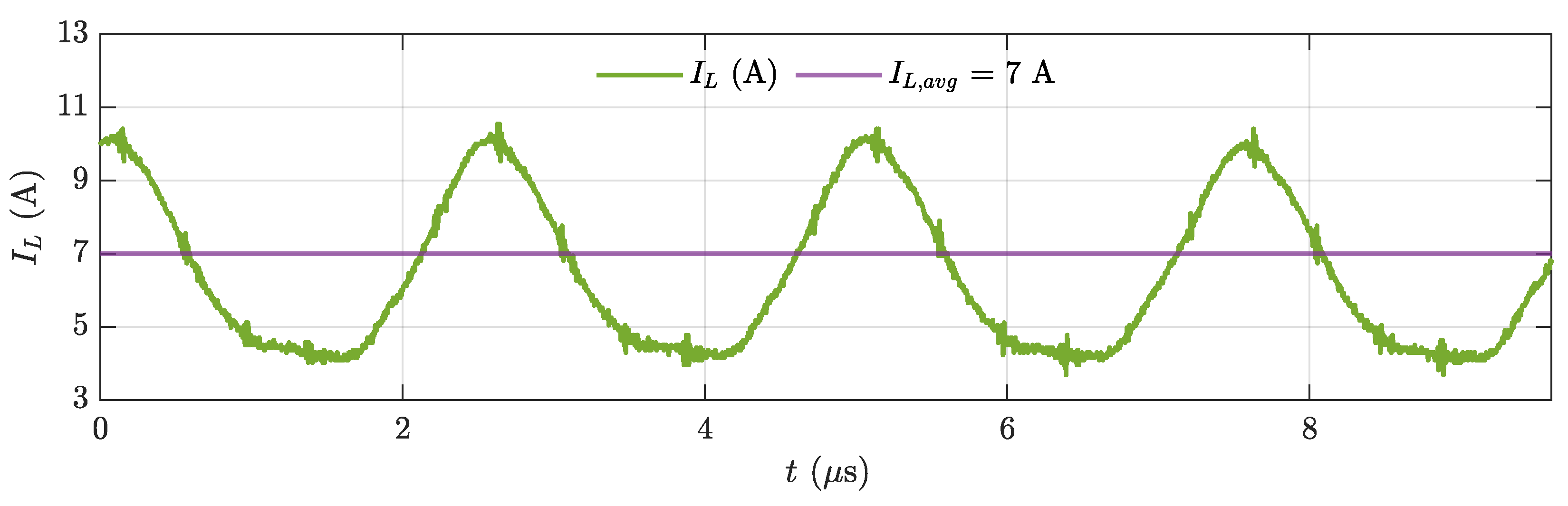
One of the most important electrical parameters assessed during the laboratory test was the inductor current. This quantity was acquired by connecting an oscilloscope probe to the output of the current-sense amplifier on the converter board.
Figure 14 shows the measured waveform of the inductor current when the converter operates under the conditions reported in
Table 6.
It can be seen that the comparison of the data obtained in simulation versus the measurements indicates a () increment in the amplitude of the ripple of the inductor current due to real inductor uncertainty and board non-idealities.
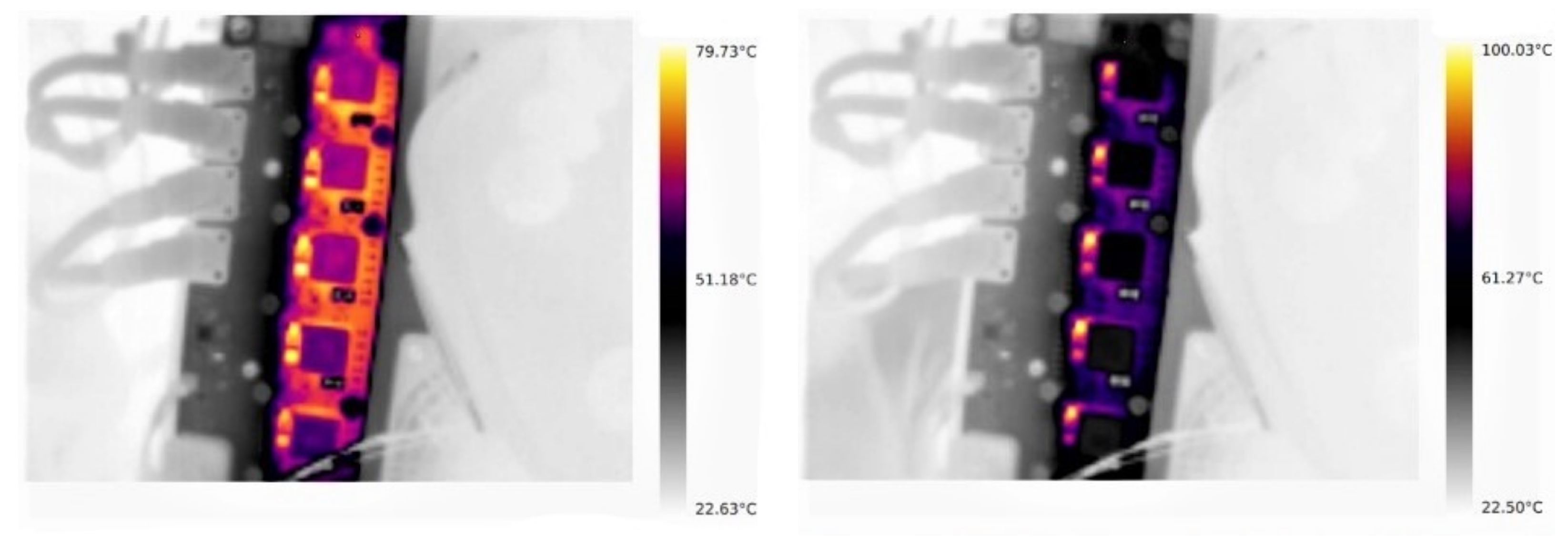
Another series of tests has concerned the verification of the cooling performance and the respecting of the temperature limits under the two synchronous and non-synchronous operating modes. The thermal camera images shown in
Figure 15 were taken in steady-state conditions and with the fuel-cell case at
.
In non-synchronous mode, the high-side mosfet, which practically works as a diode, is the most stressed component. In said condition, this component reaches . In synchronous mode, instead, the loss, and thus the heat, are distributed evenly over both mosfets of each phase. This operating mode allows the temperature to be lowered by compared to the non-synchronous mode.
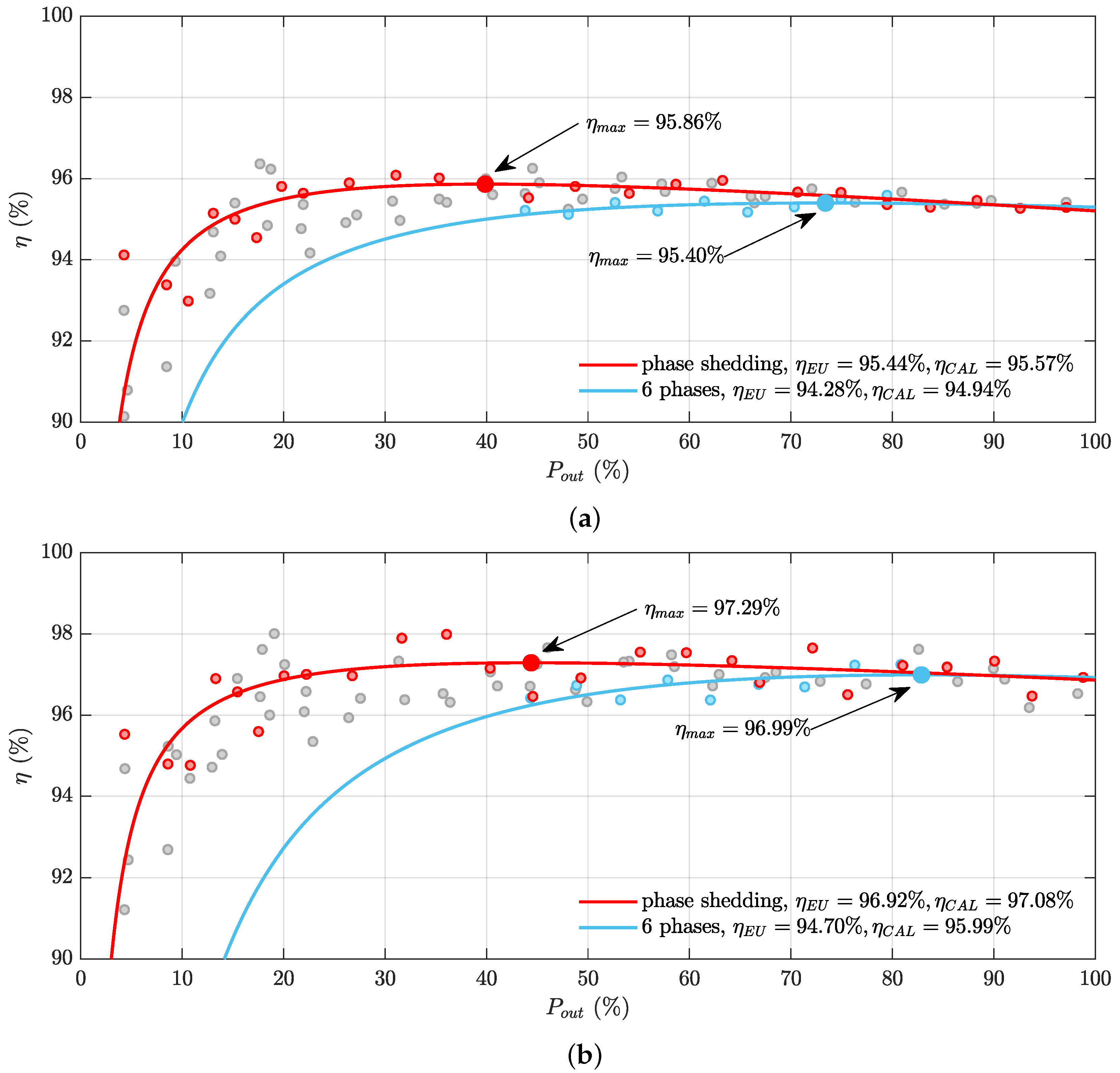
The results related to the converter efficiency in the different operating modes are summarized in the graphs of
Figure 16.
Tests were conducted by increasing the number of active phases with the increase in the output power of the converter. In this way, multiple efficiency traces were achieved, and the effectiveness of the phase shedding technique was readily validated. Each phase was rated
(i.e.,
of the total rated power of the converter of
). Nevertheless, the tests were performed for a short time above the rated value to increase the experimental dataset’s range. For
Figure 16, the experimental data, indicated with the colored circles, were interpolated to provide a continuous indication of the trend in efficiency as the number of active phases increases. These validations were carried out for both non-synchronous (see
Figure 16a) and synchronous modes of operation (see
Figure 16b). The observations indicate that during low-power operation, the use of a limited number of phase converters (one or two phases) provides better efficiency than operating with all six phases. In contrast, the use of more phases for a power closer to the rated level allows for an almost flat efficiency profile.
For a more immediate and clear visualization of the results,
Figure 17 shows the efficiency trend in the case of permanent use of all six phases and in the case of the use of the phase shedding technique.
The interpolation for the phase shedding was computed bearing in mind that each leg can withstand at most 1/6 of the rated power; this means that only points displayed as red dots were eligible for the calculation. This assumption was made to preserve each active phase within the range of its maximum local efficiency [
57]. The efficiency trace related to all six phases is identical to the one visible in
Figure 16. In this case, a
difference between the non-synchronous (
Figure 17a) and synchronous (
Figure 17b) modes of operation can be observed. During low-power operation, the efficiency improved by a few percentage points between phase shedding and six phases used in both operating modes.
Table 7 provides European (
) and Californian (
) efficiencies [
58], together with the maximum experimental and interpolated points. In this way, multiple figures of merit are provided, ensuring overall efficiency assessment in both modes of operation.
In the case of non-synchronous mode, the is higher with the use of phase shedding. Similarly, a difference can be seen in the case of . Moreover, a difference lower than can be seen for the maximum efficiency value () calculated from experimental data () and from interpolated data (). On the other hand, phase shedding in synchronous mode resulted in and being and higher, respectively, than the continuous operation with all six phases. This demonstrates the effectiveness of the phase-shedding technique.
In conclusion, phase shedding’s effectiveness was assessed for both synchronous and non-synchronous modes. In particular, synchronous mode proved to be more efficient at all working points and in all operating modes.
6.2. In-Field Test
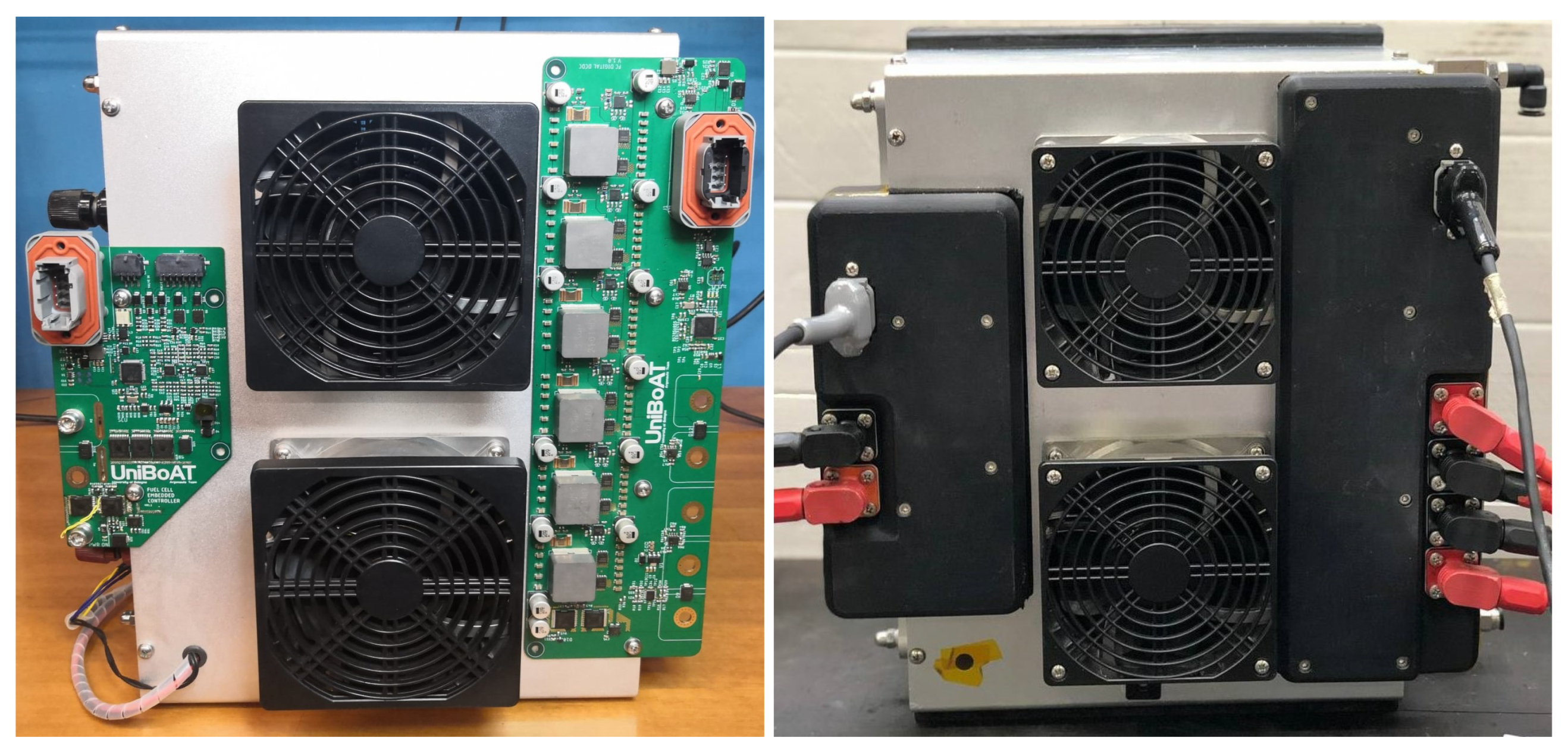
The resulting complete prototype composed of the fuel-cell stack, the controller (with the SCU inside) and the DC-DC converter is shown in
Figure 18.
The electrical and electronic parts were equipped with automotive-grade connectors and enclosed inside 3D printed covers specifically designed to guarantee equivalent IP66 protection. The data during the boat cruising were collected by means of a vehicle control unit (VCU). The VCU recorded all operating variables at and provided different log files that were imported in Matlab for the offline analysis of the performance in the real case scenario.
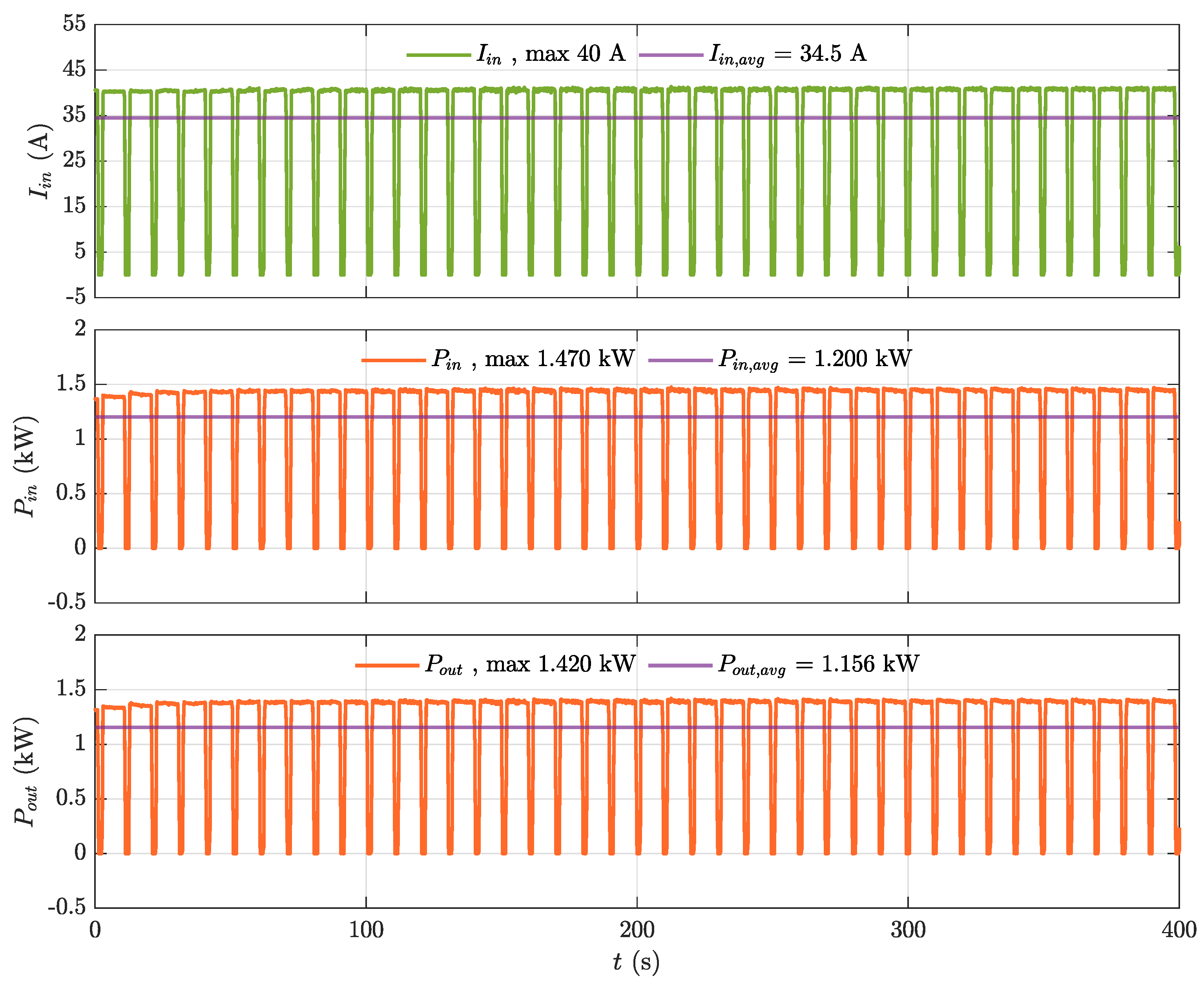
Figure 19 shows the input current, input power and output power waveforms measured by the DC-DC MCU and transmitted to the VCU through the CAN bus.
The input-current behavior highlights the intervention of SCU. When SCU is about to take action, the FC controller notifies the DC-DC converter that a short circuit is going to occur. Then, the DC-DC switches are turned off and the back-to-back input mosfets open. Once the SCU intervention period is over, the DC-DC automatically returns to operating normally. Naturally, this cyclic operation causes a decrease in the average power delivered by the fuel cell, as can be noticed by observing the power waveforms.
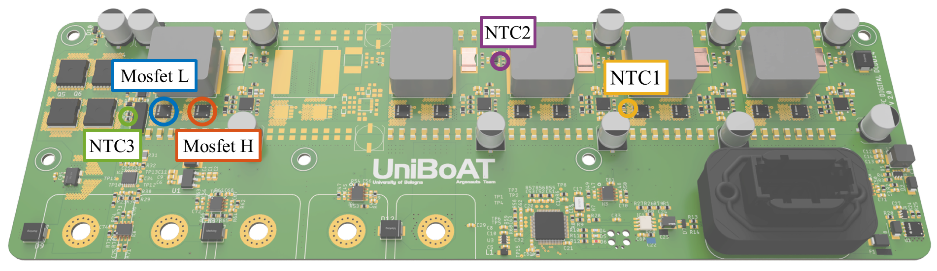
The operating temperatures were continuously monitored by means of two NTC sensors glued with thermal compound to the first phase mosfets and other three SMD NTCs installed directly on the PCB, as shown in
Figure 20.
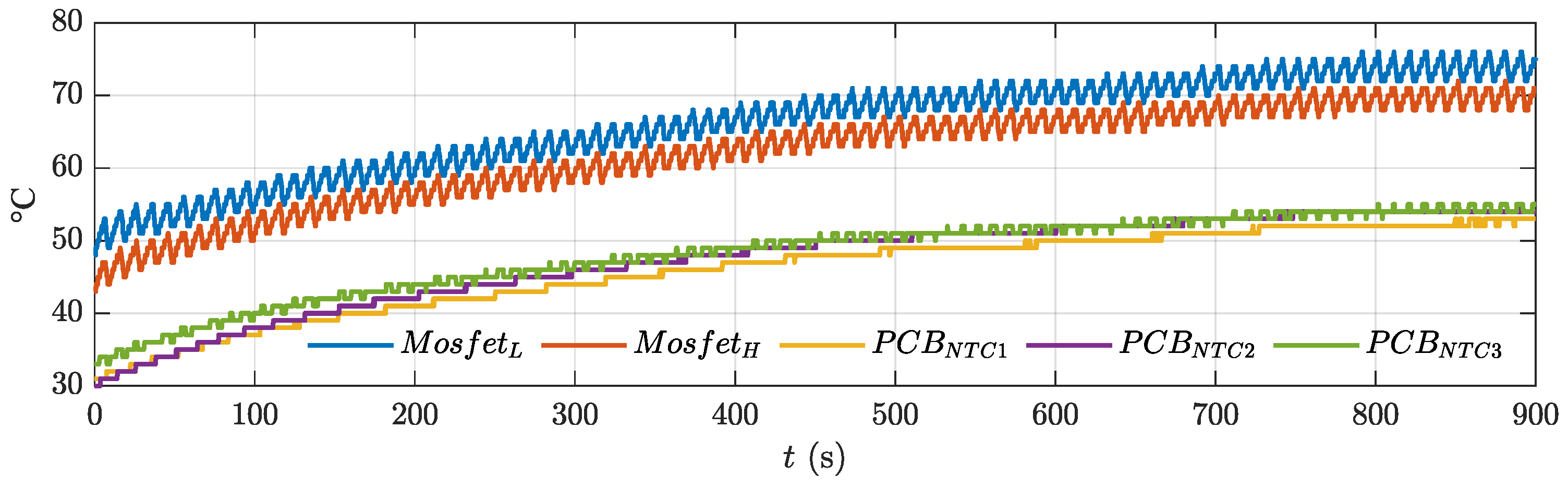
The measured temperatures are shown in
Figure 21. At steady-state, all the temperatures were verified to be below the ratings of the components with an adequate margin. These results demonstrated good performance of thermal dissipation.
The results obtained from the two tests and the different set of working conditions are summarized in
Table 8.
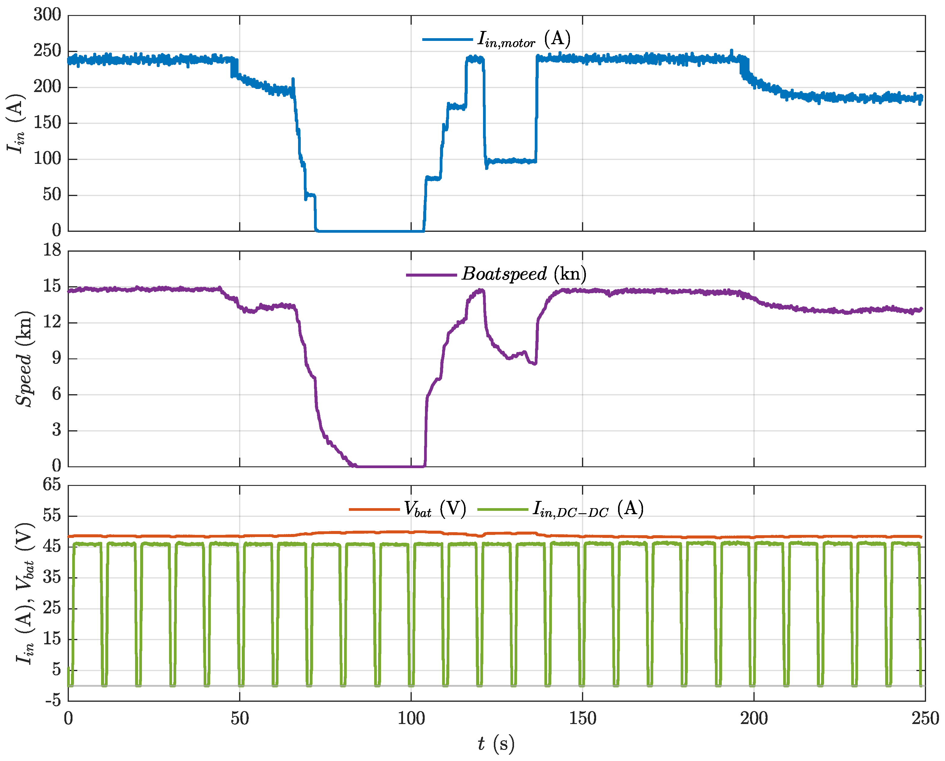
Figure 22 shows the motor current, the boat speed, the battery voltage, and the converter’s input current obtained during the sea trial cycle used to test the whole boat power and traction chain.
The rapid changes in the speed that mirror fast transients in the motor current are due to the boat’s acceleration, deceleration, and veering. The motor current goes to zero during the period of stopping of a few tens of seconds. It can be noticed that a slight variation in battery voltage (
) occurs in correspondence with the motor current variation. Despite the input/output voltage variation or load current variation, the converter input current (
-
) is always kept constant at the rated value. Even in the real data shown in
Figure 23, the fuel cell power is clearly kept constant while the battery power is changing in accordance with the motor’s behavior. This proves the better performance of the regulator during the load transients.
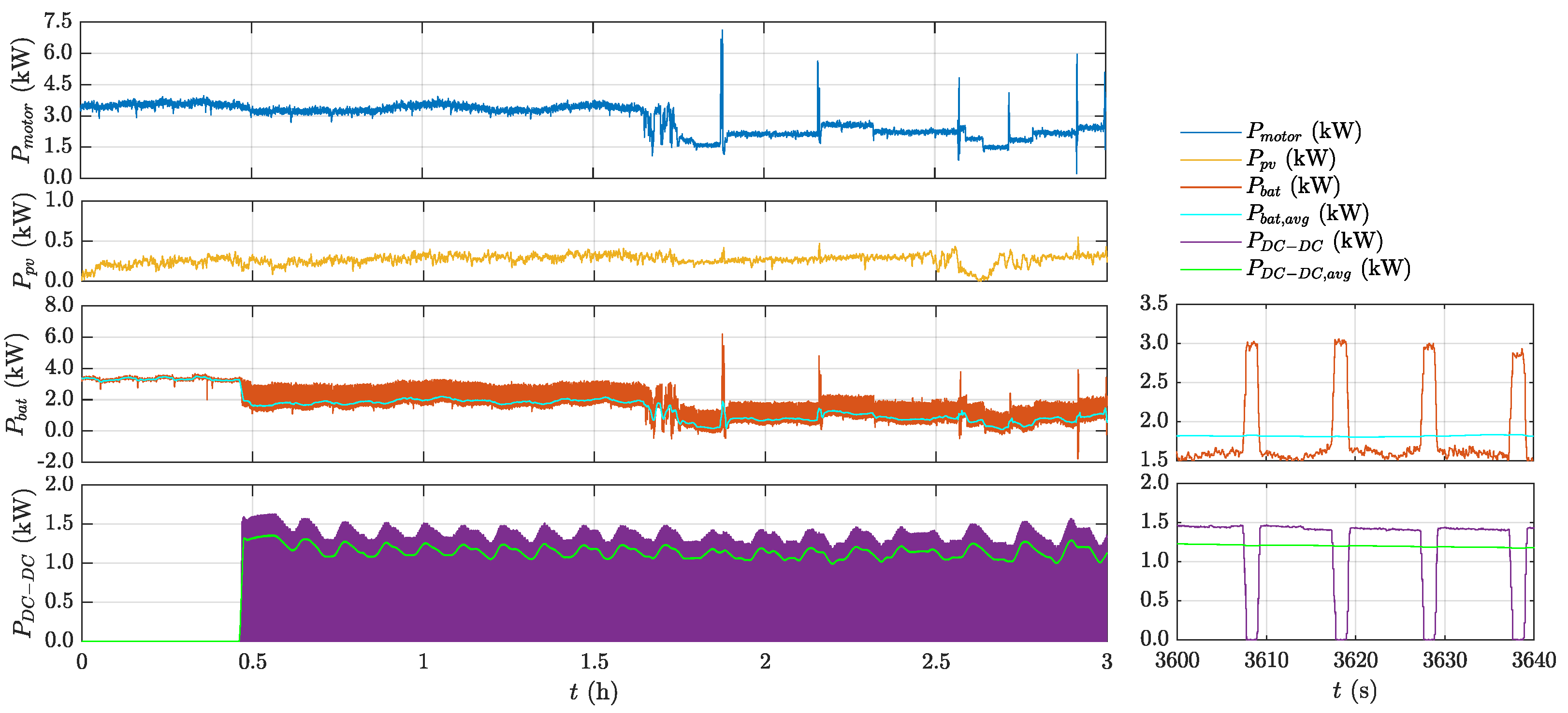
Figure 23 is reported to provide a comprehensive view of the power chain power flows. The shown data were collected during the endurance race held for 3 h. In the first half-hour phase of the race, the fuel cell was not used in order to preserve the limited amount of hydrogen stored in the tanks onboard that was instead used in the subsequent two and half hours. Consequently, the power associated with the FC (
-
) was zero. Therefore, the power provided to the motor (
) during the first phase was a combination of battery (
) and PV (
) power. The majority of the power of the first phase was provided by the battery. This allows one to keep the DC bus voltage as high as possible to avoid absorbing a high current from the battery once a lower state of charge is reached. This helps to preserve the battery’s health. When the FC starts contributing, a reduction in power provided by the battery can be observed. It is more clearly visible from the moving average plot (
) calculated by considering an averaging window width of
. This assumption was made based on the interval of SCU action. A magnification of the plots was provided to show how the full power for the traction is provided by the battery during each SCU activation.
About half way through the race, the motor power was reduced to preserve the total energy for the next races mentioned in the introduction. The fuel cell was operated at the rated value in the entire race; therefore, a reduction in battery power was observed during this period. The sharp load transients visible in
Figure 23 occurred for various reasons, such as avoiding dangerous situations while sealing and fast overtakes.
7. Conclusions
The boost DC-DC converter discussed in the present work was demonstrated to fulfill the design specifications and proved to be reliable when working both in the laboratory and in real operating conditions during navigation and competition.
Thanks to the choice of high-performing electrical components and the extensive analysis of the PCB layout, the switching frequency could be kept high without compromising the whole converter’s performance. This, along with the optimized FW and control strategies, made it possible to realize a lightweight () and efficient () converter.
The digital implementation of the ACMC precisely regulated the FC current, which followed the reference set-point even in the presence of the fast variation caused by the presence of the SCU operation. The common drawback of ACMC’s inability to perform cycle-by-cycle overcurrent protection was completely overcome by using specifically designed fault circuitry and low-latency MCU input lines.
The converter’s modularity is now under study to achieve a higher FC power rating employing the same base structure discussed in this paper. In this way, technological transfer and industrialization for applications not strictly related to naval racing that could take advantage of the great power density ensured by using FC case as a converter heat sink could be enabled by taking advantage of the scale economy.


 ,
, 


