Article

Evaluation of Microwave Characterization Methods for Additively Manufactured Materials

Wolfson School of Mechanical, Electrical and Manufacturing Engineering, Loughborough University, Loughborough LE11 3TU, UK
*
Author to whom correspondence should be addressed.
Designs 2019, 3(4), 47; https://doi.org/10.3390/designs3040047
Submission received: 31 July 2019 / Revised: 19 September 2019 / Accepted: 20 September 2019 / Published: 25 September 2019
(This article belongs to the Special Issue 3D-Printed RF Devices and Antennas)

Abstract

:
Additive manufacturing (AM) has become more important and common in recent years. Advantages of AM include the ability to rapidly design and fabricate samples much faster than traditional manufacturing processes and to create complex internal geometries. Materials are crucial components of microwave systems and proper and accurate measurement of their dielectric properties is important to aid a high level of accuracy in design. There are numerous measurement techniques and finding the most appropriate method is important and requires consideration of all different factors and limitations. One limitation of sample preparation is that the sample size needs to fit in the measurement method. By utilizing the advantage of additive manufacturing, the material can be characterized using different measurement methods. In this paper, the additive manufacturing process and dielectric measurement methods have been critically reviewed. The test specimens for measuring dielectric properties were fabricated using fused filament fabrication (FFF)-based additive manufacturing and were measured using four different commercial dielectric properties measurement instruments including split post dielectric resonator (SPDR), rectangular waveguide, TE01δ cavity resonator, and open resonator. The measured results from the four techniques have been compared and have shown reasonable agreement with measurements within a 10 percent range.

1. Introduction

Additive manufacturing, more commonly known as 3D printing, is a method of manufacturing and rapid prototyping defined as a process of joining materials to make objects from 3D model data, usually layer upon layer, as opposed to subtractive manufacturing methodologies [1]. 3D printing is beginning to be widely used for radio frequency (RF) applications. Therefore, it is essential to obtain accurate electromagnetic properties of the 3D-printed materials before using them.
In order to fully characterize the electromagnetic properties of a material in a precise and accurate way, it is advantageous to use more than one method of measurement. For research and development purposes, AM (Additive manufacturing) processes offer a significant advantage compared to traditional RF and microwave sample fabrication methods such as casting, pressing, and injection molding. Each measurement technique will typically require different material dimensions and geometries. With traditional manufacturing processes, these individual requirements can delay fabrication due to retooling requirements with low production runs becoming high cost [2]. However, with 3D printing, a computer-aided design (CAD) model can be created to the chosen characterization technique’s required dimensions and geometry.
Measurements of 3D printing over broad frequencies from 1 MHz to 11 GHz were studied in [3]. Three different methods including inductance, capacitance, and resistance (LCR) meter, impedance analyzer, and X-band waveguide were used for the dielectric properties measurement. The 3D-printed materials are viable options for future RF and microwave devices based on the measurements that were performed. Transmission lines using 3D printing equipment were fabricated and shown to be comparable in performance to traditional manufacture in [4]. The measurement results demonstrated that 3D printing is a good option for fabrication of RF/microwave components by utilizing the advantages of the design flexibility, compactness, and fast manufacturing.
The Internet of Things requires antennas to be integrated into different factors and next to different materials. In parallel to this, there is the need to create extra degrees of freedom for the RF engineer to improve performance by developing bespoke dielectric materials [5], graded dielectric properties, or 3D shapes [6]. 3D printing allows the flexibility to design air inclusions in the dielectric host. If these inclusions are much smaller than a wavelength, then the material behaves as an artificial dielectric which is a class of nonresonant metamaterial. By varying the internal air volume, the dielectric properties can be varied from ε r ~1 up to the relative permittivity of the bulk material [7,8]. Alternatively, if the air inclusions are replaced by small metallic inclusions, the relative permittivity of the artificial dielectric can be increased [9]. Using such techniques enables 3D printing to vary the dielectric properties across the surface of the device. This can be exploited to create flat graded index lenses to increase the gain of an antenna [10].
In this paper, the objective is to validate the measurement results of the 3D printing samples using different microwave characterization methods. Microwave characterization methods basically are classified into two categories: nonresonant and resonant. Section 2.1 gives a detailed description of those methods in the nonresonant category while Section 2.2 discusses those methods in the resonant category. In Section 3, four commercial measurement methods including SPDRs, rectangular waveguide, TE01δ cavity resonator, and open resonator are presented. Materials under test (MUTs) fabricated from 3D printing were prepared and measured in Section 4 and the measurement results were compared between these commercial measurement methods and analyzed. In Section 5, the conclusions are described at the end of this paper.

2. Microwave Characterization Methods

A material that has the capability of storing energy when there is an external electric field applied is classified as dielectric. Dielectric materials play an important role in various engineering fields and accurate measurement of their properties is important to design the next generation of antennas and radiofrequency (RF) components. The main parameter of dielectric properties is absolute permittivity ε and is expressed as in Equation (1) where ε 0 is called the permittivity of free space and ε r is the relative permittivity.
ε = ε 0 · ε r = ε 0 ( ε r j ε r )
The permittivity of free space ε 0 = 8.854   × 10 12 F/m. The relative permittivity ε r is a complex number including the real part ε r , which shows how much energy from an external electric field is stored, while the imaginary part ε r represents how dissipative or lossy this material is to an external electric field. The real part of the relative permittivity is often called dielectric constant even though it is not a constant; it changes with temperature, frequency, orientation, mixture, pressure, and so forth. The imaginary part of the relative permittivity is often called the loss factor. The ratio of the energy lost to the energy stored is called the loss tangent or tan δ as presented in Equation (2). In this paper, the measurement results of dielectric properties that will be discussed are primarily the dielectric constant and loss tangent.
l o s s   t a n g e n t = t a n   δ = ε r ε r
Among all the dielectric property measurement methods, it is true that no single method can characterize the dielectric properties of all materials. Uncertainty always exists in characterization. Finding the suitable measurement method is critical for the acquirement of material properties. In addition, there are still many sample shapes that are difficult to measure, especially for specific frequency bands.

2.1. Nonresonant Methods

In nonresonant methods, the properties of the material are deduced from the reflection or reflection/transmission data. The data of the transmission and reflection are obtained through the vector network analyzer (VNA) [11,12]. In general, all types of transmission lines such as coaxial line, hollow metallic waveguide, dielectric waveguide, and free space are able to be used in the nonresonant methods [13]. Nonresonant methods mainly include the reflection methods and the transmission/reflection methods. The difference is transmission/reflection methods need both the reflection and transmission data to deduce the properties of the material while the reflection methods require only the reflection data.

2.1.1. Reflection Methods

In the reflection methods, the MUT is introduced into a certain position of the transmission line. The impedance loading to the transmission line changes and the properties of the MUT can be deduced from the reflection due to the changed impedance.
One of the most used reflection methods is called coaxial probe method. It is also known as coaxial-line probe, open-ended coaxial line, or open-ended coaxial probe method. The probe or sensor is the measurement fixture in the transmission line. It is important because it decides the accuracy and sensitivity of the measurement. Different probes are made according to different measurement requirements, but they need different calculation algorithms [13].

2.1.2. Transmission/Reflection Methods

In the transmission/reflection methods, the MUT is placed in the transmission line or waveguide. The relative permittivity and permeability of the MUT are deduced from the data of the transmission and reflection. A general procedure used for the dielectric property measurement is: Set up vector network analyzer → set the frequency range/number of points → measure sample dimensions → calibrate system → place MUT on fixture → measure S-parameter → perform calculation → display complex permittivity and permeability [14]. In the calculation procedure, the Nicolson–Ross–Weir (NRW) algorithm is usually the basic and the most common method [15,16]. This algorithm can deduce the permittivity and permeability from the scattering parameters of the transmission and the reflection.
Two types of commonly used transmission/reflection methods are the hollow metallic waveguide method and the free space method. The hollow metallic waveguide method includes the rectangular and circular waveguides. The rectangular waveguides are used more widely, and the waveguides are classified to different working bands with minimum and maximum frequency limits for each band.
The other commonly used transmission/reflection method is the free space method. Compared to the hollow metallic waveguide method, it does not need to consider if the MUT can be fitted in the waveguide cross-section or not. It is suitable for nondestructive and contactless dielectric measurement of the MUT, and the setup was demonstrated by Ghodgaonkar et al. in [17]. However, the sample had to be larger than ten wavelengths and often had to use time-gating to stop reflections off walls.

2.2. Resonant Methods

Compared to the nonresonant methods, the resonant methods have a higher accuracy and sensitivity. However, they are limited to a single or several discrete frequencies. Sheen conducted a systematic study on different resonant methods for measurement of dielectric properties and suggested how to choose a suitable resonant measurement method [18]. The resonant methods include the MUT as a resonator method and resonant perturbation method. The difference between the MUT as a resonator method and resonant perturbation method is the latter deduces the properties of the MUT by the change of the resonant properties while the former uses the resonant properties.

2.2.1. MUT as a Resonator Method

The MUT is taken as the resonator or a key part of a resonator in these methods. The properties of the MUT are deduced from the resonant properties of the resonator. Hakki and Coleman created a technique for the measurement of dielectric and magnetic properties by using a cylindrical dielectric rod as a resonator and putting it between two parallel conducting plates. The results of the measured dielectric constant had a less than 0.2 percent difference from the literature values [19]. Courtney later analyzed and developed Hakki and Coleman’s method to an improved one that could obtain the dielectric loss tangent with an error less than 5   ×   10 5 [20]. This method is now well known as the “Courtney method”.

2.2.2. Resonant Perturbation Methods

In the resonant perturbation methods, the MUT is introduced into a resonant structure and the properties of the MUT are determined from the change of the resonant properties. Hollow metallic cavities are often used in the perturbation methods and it is called the cavity perturbation method. The perturbation theory and formulas of resonant cavities were studied and discussed by Waldron in [21]. Dube et al. examined the cavity perturbation method in the X-band waveguide [22]. They concluded that the cavity perturbation method was convenient and accurate for the measurement of dielectric properties. They also simplified the perturbation equations to obtain the dielectric constant and loss tangent by putting the sample at the maximum electric field location in the rectangular waveguide cavity. The perturbation formulas were discussed in more detail for the use in the resonators and waveguides by Waldron to identify when the formulas were applicable [23]. The paper proved that the formulas were limited when the frequency shift was small.

3. Commercial Methods for Characterization

Four kinds of commercial dielectric properties measurement instruments were used for the measurements of 3D-printed MUTs in this paper. They are: (i) split post dielectric resonator from QWED Company, Warsaw, Poland (resonant perturbation method), (ii) rectangular waveguide (transmission/reflection method), (iii) open resonator: Model 600T from Damaskos, Inc., Concordville, PA, USA (resonator method), and (iv) cavity resonator: TE01δ Mode Dielectric Resonator from QWED Company, Warsaw, Poland (resonator method). In this section, the details of these instruments are described.

3.1. Split Post Dielectric Resonator (SPDR)

The concept to utilize the SPDR was first introduced by Nishikawa et al. in 1988 [24]. Two dielectric resonators were separated by the space where the MUT was placed. Relative permittivity and loss tangent of the MUT were calculated from the measurement of frequency perturbation. However, the calculation equations were provided from perturbation theory of the small dielectric objects in the cavity and therefore the thickness of the MUT was not considered in the calculation. Later, in 1996, Krupka et al. developed an improved SPDR method where the thickness of the MUT was included in the calculation equations [25]. Relative permittivity and loss tangent of the MUT were able to be deduced from Equations (3) and (4).
ϵ r = 1 + f 0 f s h f 0 Κ ϵ
where:
  • h is the thickness of the MUT;
  • f 0 is the resonant frequency of the empty SPDR;
  • f s is the resonant frequency of the SPDR with MUT;
  • Κ ϵ is a function of ϵ r and h, and has been evaluated for a number of ϵ r and h using the Rayleigh–Ritz technique. For a practical approach, a number of ϵ r and h were used for computing the exact resonant frequencies and the values of Κ ϵ , then the whole results were tabulated.
t a n   δ = 1 p e s ( 1 Q 0 1 Q D R 1 Q c )
where:
  • pes is the electric energy filling factor for the MUT;
  • Q0 is the unloaded Q-factor of the resonator with MUT;
  • QDR is the Q-factor depending on dielectric losses of the empty resonator;
  • Q c is the Q-factor depending on metal enclosure losses of the empty resonator.
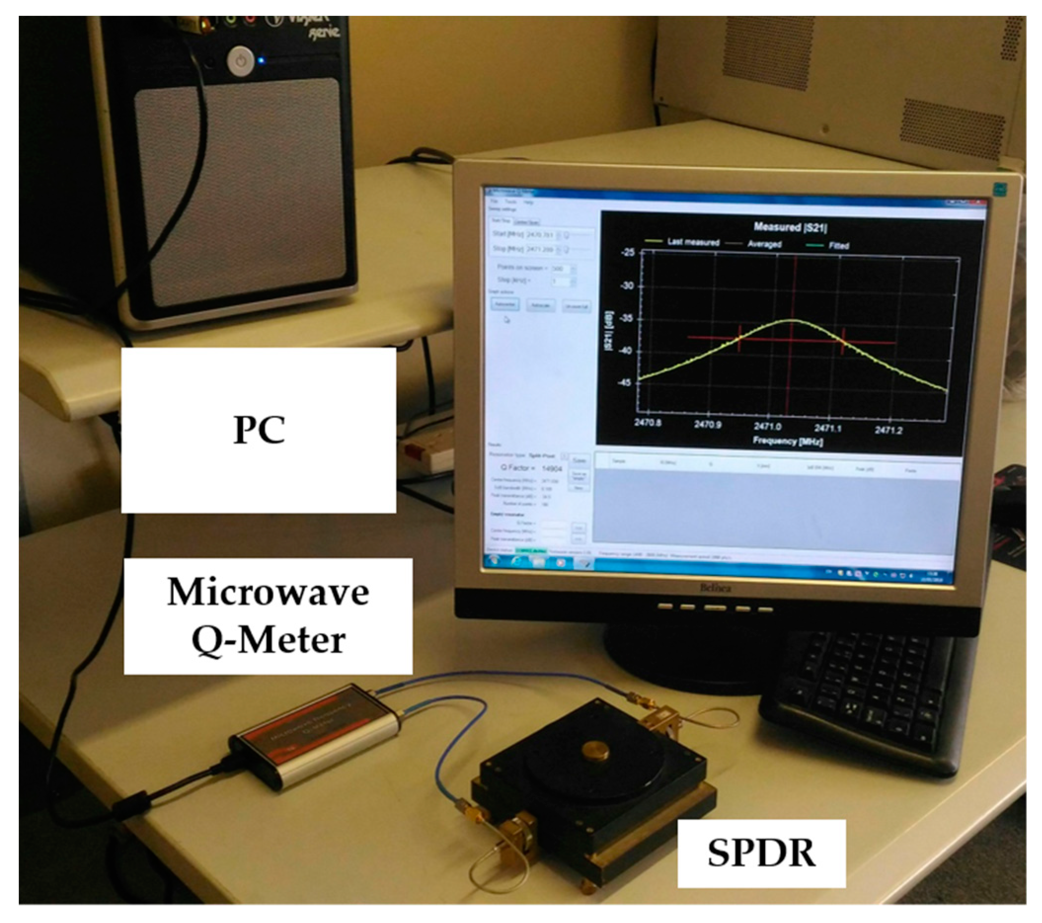
By using a 4 GHz SPDR, Krupka et al. proved the measurements of well-machined laminar dielectric specimens could obtain uncertainties down to 0.3% for relative permittivity and 2   × 10 5 for loss tangent [26]. More studies of measurements using SPDR were presented in [27,28,29,30]. In 2012, Korpas et al. introduced the “Microwave Q-Meter”, which was a replacement for the VNA normally used with the SPDR [31] as shown in Figure 1a. The requirement of the VNA is avoided by using the Microwave Q-meter that brings researchers more convenience and cost savings. However, different SPDRs need their specific program settings and corresponding Microwave Q-Meters to extract the dielectric constant and loss tangent of the MUT. The MUT is placed into the SPDR between the top (black) and bottom (brown) plates, and in the center of the SPDR (yellow square) as shown in Figure 1b. The complete SPDR measurement system is demonstrated in Figure 2.
Each SPDR can only provide dielectric properties at a single frequency and cannot measure the magnetic properties. The minimum size, maximum width, and thickness of the MUT are constrained by the SPDR operating frequency and fixture structure. Meanwhile, the thickness of the MUT must be uniform. There were three different frequency SPDRs (1.1 GHz, 1.9 GHz, and 2.4 GHz) used in this paper. The minimum size, maximum width, and thickness of the MUT for each SPDR are shown in Table 1 [32].

3.2. Rectangular Waveguide

Rectangular waveguide is one of the most commonly used instruments for the measurement of dielectric properties. It is the typical type of the transmission/reflection method as previously discussed in Section 2.1.2. The X-band (8.2–12.4 GHz) rectangular waveguide measurement instrument at Loughborough University is shown in Figure 3. The X-band rectangular waveguide limits the measurement frequency to between 8.2 GHz and 12.4 GHz. The MUT size must be exactly the same as the X-band rectangular waveguide aperture, which is 22.86 × 10.16 mm. At the same time, the thickness of the MUT must be uniform. The MUT is inserted into the aperture of the flange. The flange is connected to the waveguide and the waveguide halves are closed until sealed. The scattering parameters S11 and S21 are obtained via the VNA and MUT dielectric constant and loss tangent are then calculated in the conversion method. Note: S11 stands for reflection coefficient and S21 represents the forward transmission.
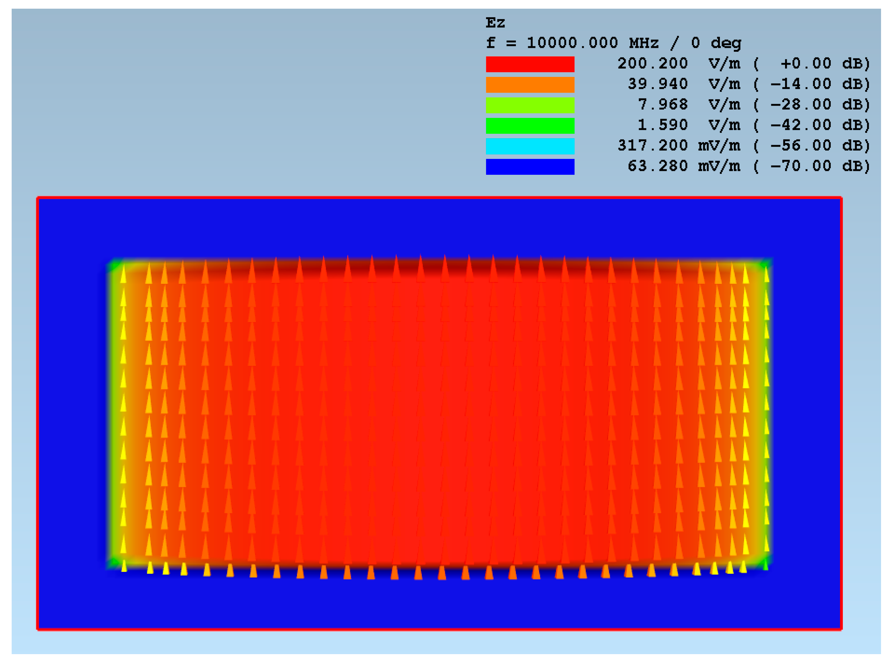
The electric fields are largest at the center along the long edge; see Figure 4. This means an air gap between the MUT and the waveguide along the top or bottom of the waveguide is critical, while a gap at the sides can be tolerated with a smaller effect on the measured results. This hypothesis was tested via deliberately 3D-printing samples which were not rectangular. Accuracy is lower compared to resonant methods and is affected by an air gap between the MUT and the waveguide walls.

3.3. Open Resonator: Model 600T from Damaskos, Inc.

The Damaskos model 600T open resonator consists of two spherical mirrors mounted coaxially and the measurement is conducted by placing the MUT in the center of the cavity as shown in Figure 5. This type of resonator was introduced by Treacy in 1966 [33]. Later, in 1970, Yu used the open resonator as a new method to measure the dielectric constant and loss tangent [34]. The details of concepts, measurement procedures, equipment, experiments, and results were described. Cullen and Yu proved the uncertainty of dielectric constant to be ±0.25% for the dielectric materials polystyrene and Perspex [35]. They also provided a reliable theoretical foundation for the open resonator method of measuring the dielectric constant and loss tangent [36]. More studies about the open resonator were presented in [37,38,39,40,41].
The measurement frequency of the Damaskos model 600T open resonator is between 10 GHz and 70 GHz. The MUT size must be 120 × 120 mm to be held in the center of the resonator cavity as shown in Figure 6 and the thickness of the MUT must be uniform. The calibration time is 20 min with full range of frequencies from 10 GHz to 70 GHz. Each measurement takes more than 10 min, which is long when compared to the other three methods (one minute at most) if the full range of frequencies is required.

3.4. Cavity Resonator: TE01δ Mode Dielectric Resonator

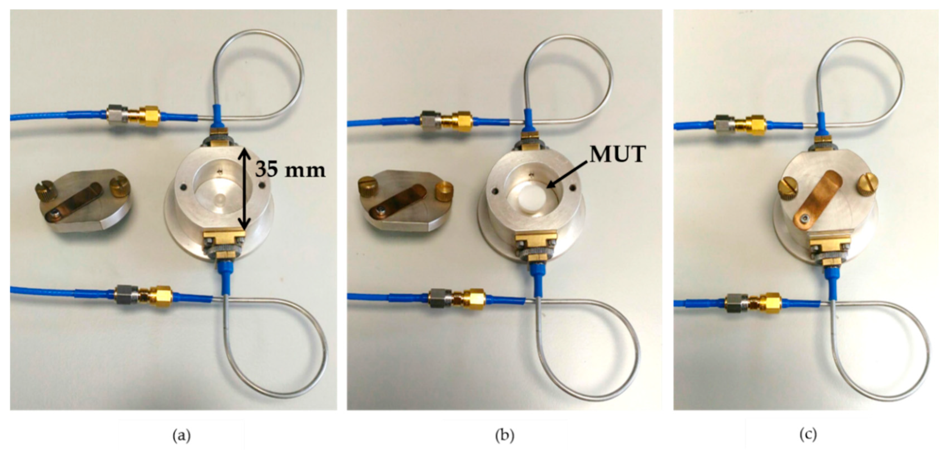
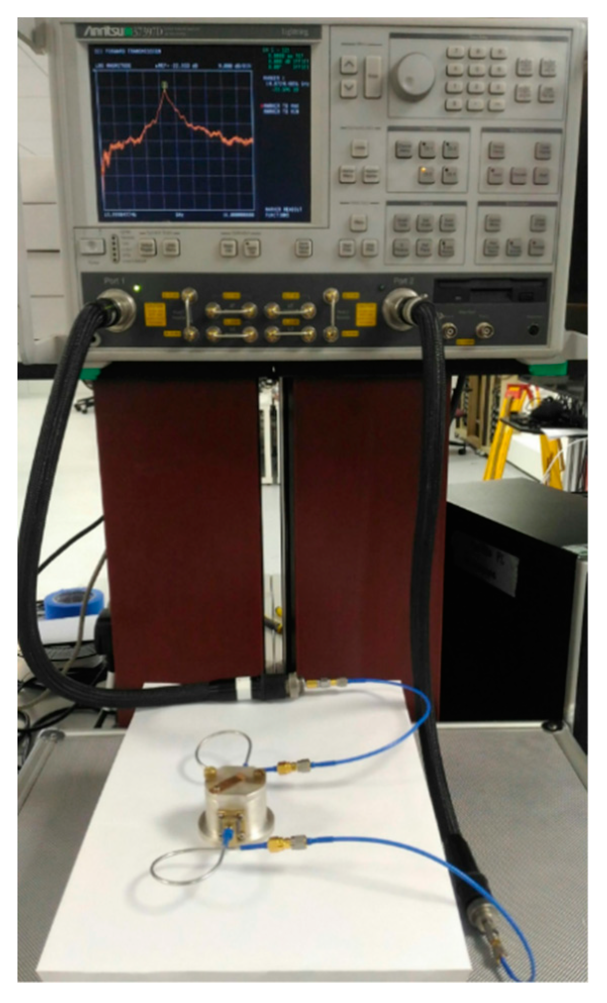
The cavity resonator has been introduced in Section 2.2.1. The TE01δ mode dielectric resonator developed by QWED company is used for precise dielectric properties measurements of disc or cylinder shape MUTs. The theory and experimental results were presented in [42] by Krupka et al. This cavity resonator provides a very accurate single-frequency measurement of relative permittivity and dielectric loss tangent for low-loss isotropic materials. However, the MUT shape needs to be a disc or a cylinder. Thinner MUTs can be stacked together to obtain the greater thickness. In principle, any cylindrical cavity has an infinite number of modes. In the cavity resonator, the first mode is generally used for the measurements of dielectric properties when the permittivity for the sample is greater than 10. The top view of the cavity resonator is shown in Figure 7a. The MUT is required to be placed at the center in the metal cavity on top of the dielectric support as shown in Figure 7b. The TE01δ mode cavity resonator is closed with the MUT inside, see Figure 7c, and the measurement system is demonstrated in Figure 8. After the resonant frequency and Q-factor of the TE01δ are measured, the relative permittivity and loss tangent of the MUT can be determined.

3.5. Summary of Commercial Methods for Characterization

Every measurement method has its own merits and limitations. Four different commercial microwave characterization methods including SPDRs, X-band rectangular waveguide, Damaskos model 600T open resonator, and TE01δ mode cavity resonator were introduced in the previous subsections.
Before characterization, sample preparation is the most obvious required factor for conducting a measurement. Therefore, good sample preparation is necessary in order to obtain an accurate and reliable measurement result. For the preparation of samples to be measured using these four commercial methods, the required sizes are shown in Table 2.
The comparison of each measurement method is summarized in Table 3. The SPDR and TE01δ cavity resonator measure in a narrow band while the X-band waveguide and Damaskos model 600T open resonator measure in a broad band. The calibrations are not needed for the SPDR and TE01δ cavity resonator due to the software provided by the device company. The time consumed by calibrations for the X-band waveguide and Damaskos Model 600T open resonator are 1 and 20 minutes, respectively, because the ranges of the measured frequency are wider. After the setup and calibration, the measurement times are all less than 1 minute except for the Damaskos Model 600T open resonator, which needs more than 10 minutes to finish the measurement.

4. 3D-Printed MUTs and Measurement Results

High tooling cost prevents the preparation of the MUT from the same material for different characterization techniques to make a fair comparison. With additive manufacturing, the manufacturer has the ability to rapidly fabricate samples and prototypes much faster than traditional manufacturing processes [43]. Therefore, in this work, the AM has been chosen to fabricate MUTs by using the same material with various dimensions that are suitable for the different microwave dielectric properties characterization techniques in the previous section. Material extrusion is a form of AM which extrudes plastics, gels, or pastes through a nozzle to build structures line by line and layer by layer. This process is generally the most inexpensive of all the additive manufacturing processes described and has the main advantage of being able to print any material that can form an extrudable plastic composite or can be dispersed into an extrudable paste. The most common form is fused filament fabrication (FFF), which extrudes molten plastics through a nozzle to form a desired shape or internal structure layer by layer. Furthermore, the FFF process has been chosen as it is currently the best developed AM process for multimaterial printing. The majority of electromagnetic components require both conductor and dielectric, therefore, as this process can currently print both dielectric and conductor simultaneously, it is important to investigate. However, although FFF has advantages with regards to multimaterial printing, it also has disadvantages with regards to part density which affects the final dielectric properties. Due to the line-by-line, layer-by-layer extrusion of plastic through a round nozzle, air gaps are created which decrease the permittivity and the loss tangent of the sample. It is therefore important to take this into account when comparing electromagnetic properties as they will typically be different from injection-molded samples made from the same materials.
To make the comparison of the characterization techniques, two commonly used 3D-printing materials were selected for fabrication via the FFF process. The first material selected was acrylonitrile butadiene styrene (ABS), a common injection-molding thermoplastic which has become popular within 3D printing due to the material’s high tensile strength and corrosion resistance [44]. The second material chosen for this demonstration was polylactic acid (PLA), which is a biodegradable bioplastic with excellent properties for 3D printing. Although PLA lacks the environmental resistance of ABS, it is widely used due to the material’s low melting point and low glass transition temperature which allows for the fabrication of complex, detailed parts in comparison to other material extrusion thermoplastics [45,46].
Both materials are not typically used for electromagnetic applications. Therefore, datasheet values are not generally supplied and when they are, they are only supplied for measurements up to 1 MHz and not microwave frequencies. Due to this, for reference, microwave measurements of injection-molded samples and 3D-printed samples must be used. Literature values for injection-molded ABS samples typically provide dielectric constant = 2.76 to 2.82 in the X-band, with 3D-printed samples providing dielectric constant = 2.74 at low microwave frequencies [47,48]. PLA is rarely used for injection molding, however, for reference, injection-molded PLA has been measured to have dielectric constant = 2.43 to 2.65 at radio frequencies [49].
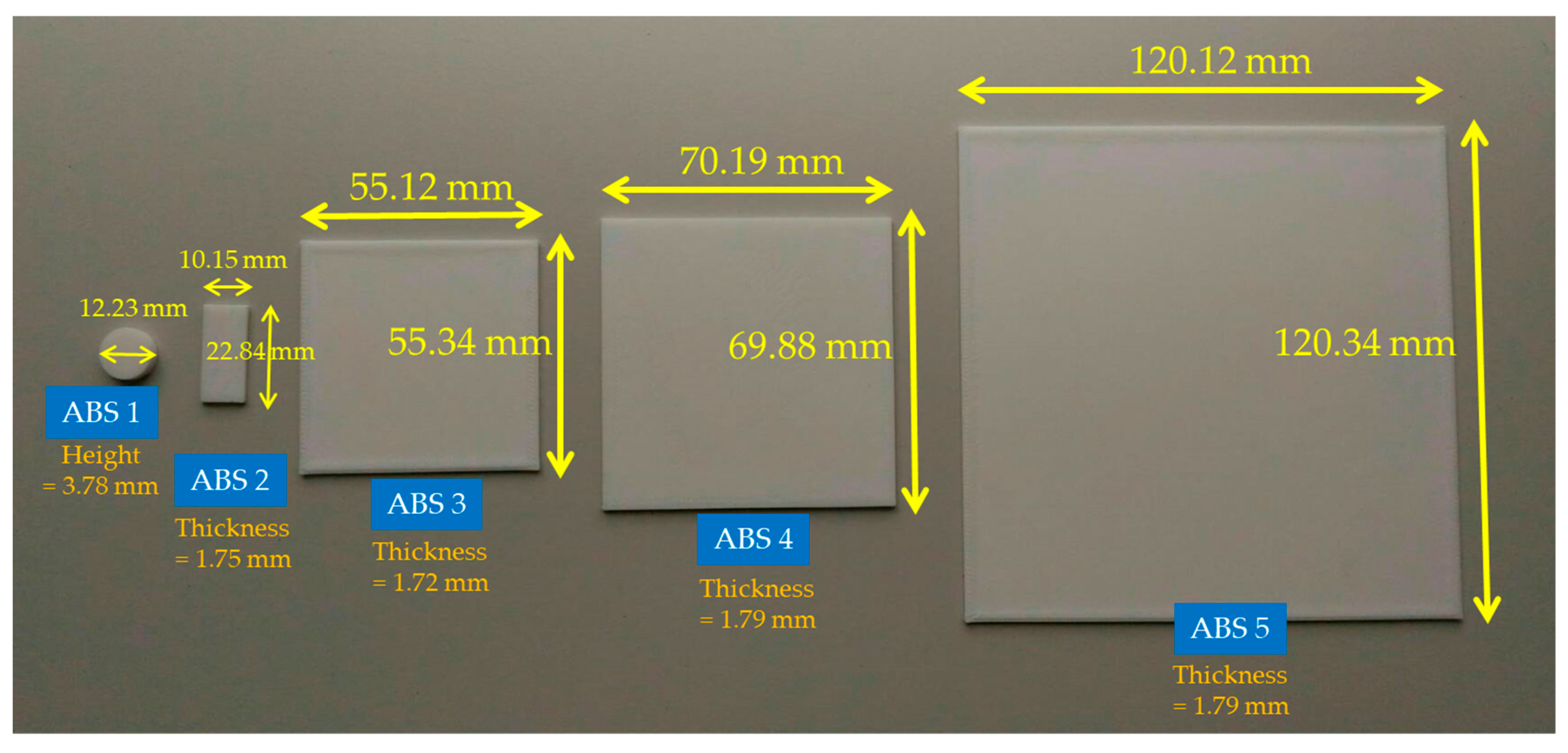
MUTs fabricated from 3D printing with ABS (Raise3D ABS, 1.75 mm) and PLA (Raise3D PLA, 1.75 mm) using a Raise3D Pro2Plus fused filament fabrication 3D printer were investigated. Four rectangles of dimensions 22.86 × 10.16 mm, 55 × 55 mm, 70 × 70 mm, 120 × 120 mm with thickness 1.5 mm and one disc of diameter 12 mm with height 3.5 mm were designed to be printed for the measurements. The printing parameters used for the fabrication of the MUTs are displayed in Table 4 and the five printed ABS MUTs are shown in Figure 9.
All samples were also printed with an initial first layer height of 0.3 mm to aid in dimensional accuracy. The thicker initial layer also aided with print bed adhesion to the BuildTak build plate. After the first layer was printed, the layer height switched to 0.2 mm layer height. Note: PLA MUTs had the same designed dimensions as the ABS MUTs.
The dielectric constant and loss tangent were measured using the SPDRs, X-band waveguide, Damaskos model 600T open resonator, and the TE01δ mode cavity resonator. MUTs named ABS 1, 2, 3, 4 were measured using the TE01δ cavity resonator, X-band waveguide, SPDR 2.4 GHz, and SPDR 1.9 GHz, respectively. The MUT named ABS 5 was measured using both SPDR 1.1 GHz and the Damaskos model 600T open resonator. Similarly, the PLA MUTs were measured using the four different characterization methods.
The fabricated size of the MUTs were different from the CAD design, which demonstrated that the accuracy of the 3D printing needs to be considered if a specific dimension is needed. Any differences are generally due to manufacturing errors. Consumer desktop FDM printers have been measured to have tolerances up to ±0.573% tolerance dependent upon CAD model geometry [50]. Other manufacturing errors can be due to shrinkage or expansion of the plastic (1 to 2% is typical), vibrations during the printing, or sections of the parts cooling at different rates.
During the measurements, many factors including dimensional accuracy, air gaps, temperature, humidity, calibration, and care of operator affect the results. The effects from these factors were minimized as much as possible. To check the repeatability of the measurement process, the measured dielectric constant and loss tangent of the MUTs were recorded twice a day over two different days. For a narrow frequency measurement using SPDRs and TE01δ mode cavity resonator methods, the variations were within ±0.02 for dielectric constant and ±0.001 for loss tangent. For a broad frequency range measurement, the mean values were calculated and the variations became larger. The variations were within ±0.05 for dielectric constant and ±0.01 for loss tangent using the X-band waveguide, and within ±0.3 for dielectric constant and ±0.02 for loss tangent using the open resonator. This demonstrated that the measurement results using the SPDRs and TE01δ mode cavity resonator methods were highly repeatable, which was expected since they were resonant methods. The X-band waveguide method was less repeatable and the open resonator had the worst repeatability due to the large cover frequency range from 8.2 to 12.4 GHz and 10 to 65 GHz, respectively.
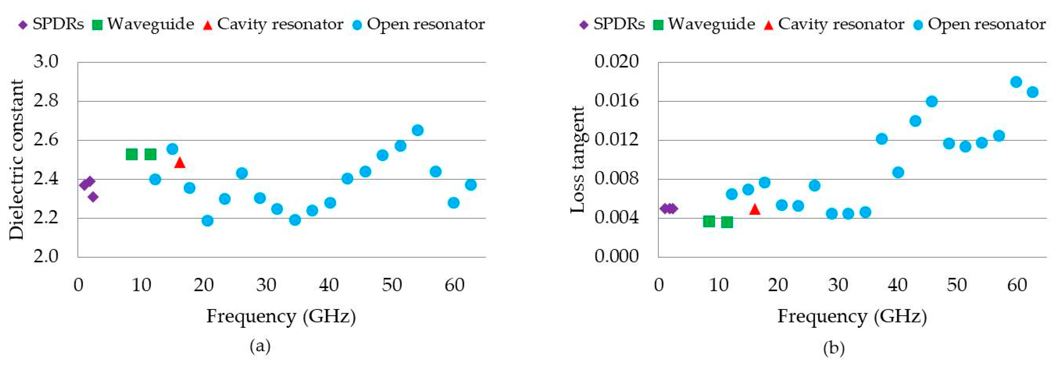
The measured ABS MUTs fabricated sizes, methods, and frequencies, together with the dielectric constant and loss tangent results, are shown in Table 5. For the X-band waveguide measurements, sample dimensions need to be accurate to 2 decimal places to prevent air gaps between the sample and sample holder which have the potential to affect dielectric constant measurements. The computer-aided design (CAD) model was designed to fit the waveguide at 22.86 × 10.16 mm exactly; fabricated sample dimensions can be seen in Table 5. When using mean values over the measured frequency range for the X-band waveguide (8.2 to 12.4 GHz) and open resonator (12.3 to 62.6 GHz), the measured dielectric constant and loss tangent from four methods of the ABS ranged from 2.37 to 2.53 and 0.004 to 0.009, respectively. Figure 10 shows the measured dielectric constant and loss tangent results at frequencies from 1.1 to 62.6 GHz using SPDRs (1.1, 1.9, 2.4 GHz), X-band waveguide (8.5, 11.5 GHz), TE01δ mode cavity resonator (16.2 GHz), and open resonator (19 resonant frequencies from 12.3 to 62.6 GHz). The variation of measurement results using the open resonator method was found to be larger than for the other three methods. This is due to the high sensitivity when measuring at high frequencies and over a large frequency range.
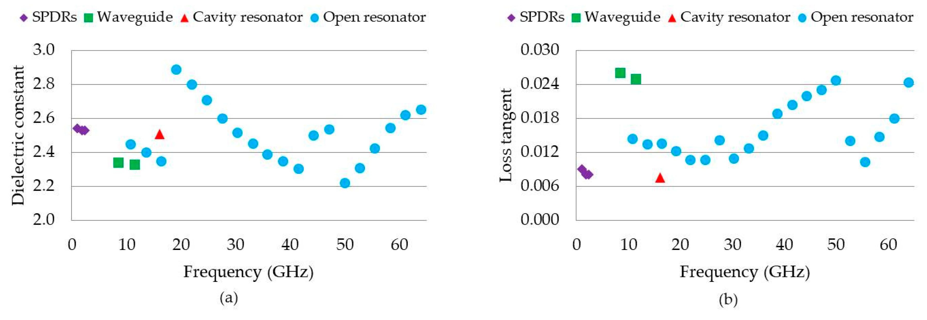
The same measurement procedures were conducted for the PLA MUTs. The measured fabricated sizes, methods, and frequencies, together with the dielectric constant and loss tangent results, are shown in Table 6. The measured dielectric constant and loss tangent results of the PLA using the SPDRs, X-band waveguide (mean values from 8.2 to 12.4 GHz), TE01δ mode cavity resonator, and open resonator (mean values from 10.8 to 63.9 GHz) ranged from 2.34 to 2.61 and 0.008 to 0.026, respectively. Figure 11 shows the measured dielectric constant and loss tangent results at frequencies from 1.1 to 63.9 GHz using the SPDRs (1.1, 1.9, 2.4 GHz), X-band waveguide (8.5, 11.5 GHz), TE01δ mode cavity resonator (16.1 GHz), and open resonator (20 resonant frequencies from 10.8 to 63.9 GHz). Overall, the measured results showed reasonable agreement with each other.
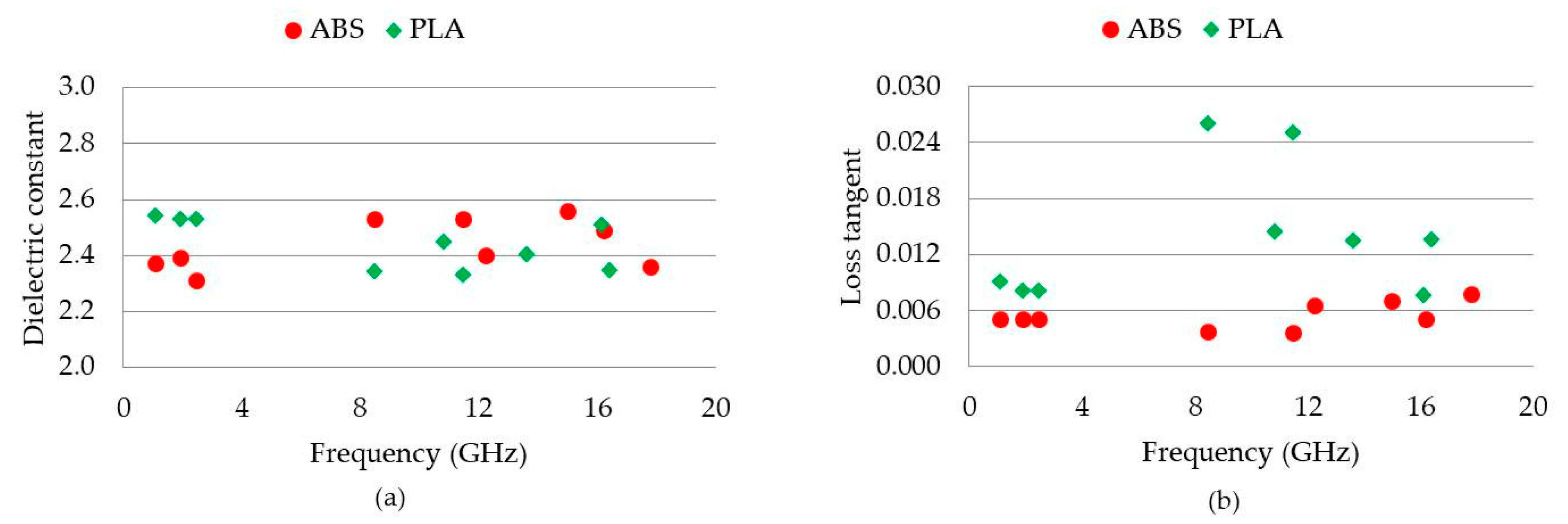
The measurement results of ABS and PLA MUTs were compared at frequencies less than 20 GHz to avoid the high variation caused by the open resonator; see Figure 12. The relative permittivity of ABS and PLA were close in the range from 2.31 to 2.61. For loss tangent, ABS had smaller measurement results than PLA over the entire frequency range. As a result, ABS is normally a better option for the fabrication of RF components due to the lower loss.

5. Conclusions

This paper has reviewed the nonresonant and resonant methods of dielectric properties measurement. In nonresonant methods, dielectric properties of the material are deduced from the reflection or reflection/transmission data, which are obtained through the VNA. This method includes coaxial line, hollow metallic waveguide, dielectric waveguide, and free space. In contrast with the nonresonant methods, the resonant methods have a better accuracy and sensitivity, but are limited to a single or several discrete frequencies.
This paper also investigated and compared four commercial dielectric properties measurement devices that include SPDRs, X-band rectangular waveguide, TE01δ mode cavity resonator, and open resonator. The MUTs from 3D printing using ABS and PLA with different sizes were prepared for the different measurement methods. The measured results were compared and showed reasonable agreement, albeit highlighting that different techniques will give different results due to the change in the geometry and frequency. The relative permittivity of the ABS samples varied from 2.31 to 2.53, while the PLA values varied from 2.34 to 2.61. The variation was within 10% for the four techniques. This demonstrates the variation in results and how different measurement systems will give different results. The ABS MUTs had loss tangents of ~0.005, while the PLA MUTs had loss tangents between 0.01 and 0.03. Hence ABS is generally a better choice for RF devices as the losses are reduced. However, PLA is generally easier to 3D print. The variability in the loss tangent results was larger than the relative permittivity. The loss tangent is always harder to measure. At higher frequencies, the wavelength becomes much smaller and hence the results are very sensitive to changes in the thickness, surface flatness, and internal structure of the MUTs.

Author Contributions

C.-K.L. and J.M. wrote the text in the paper and measured some of the MUTs. C.T. conducted other measurements while S.Z., D.C., A.G., T.W., and R.G. provided insightful advice throughout the research. D.E., J.V., and W.W. supervised and reviewed the manuscript prior to submission.

Funding

Chih-Kuo (Chuck) Lee is grateful for the financial support from the Republic of China (Taiwan) National Defense University. Additional support was provided by EPRSC grants: EP/N010493/1 (SYMETA) and EP/S030301/1 (ANISAT).

Conflicts of Interest

The authors declare no conflict of interest.

References

  1. American Society for Testing & Materials. Standard Terminology for Additive Manufacturing Technologies; ASTM International: West Conshohocken, PA, USA, 2012. [Google Scholar]
  2. Franchetti, M.; Kress, C. An economic analysis comparing the cost feasibility of replacing injection molding processes with emerging additive manufacturing techniques. Int. J. Adv. Manuf. Technol. 2017, 88, 2573–2579. [Google Scholar] [CrossRef]
  3. Deffenbaugh, P.I.; Rumpf, R.C.; Church, K.H. Broadband microwave frequency characterization of 3-D printed materials. IEEE Trans. Compon. Packag. Manuf. Technol. 2013, 3, 2147–2155. [Google Scholar] [CrossRef]
  4. Deffenbaugh, P.I.; Weller, T.M.; Church, K.H. Fabrication and Microwave Characterization of 3-D Printed Transmission Lines. IEEE Microw. Wirel. Components Lett. 2015, 25, 823–825. [Google Scholar] [CrossRef]
  5. Bukhari, S.S.; Whittow, W.G.; Zhang, S.; Vardaxoglou, J.C. Composite materials for microwave devices using additive manufacturing. Electron. Lett. 2016, 52, 832–833. [Google Scholar] [CrossRef] [Green Version]
  6. Motevasselian, A.; Whittow, W.G. Miniaturization of a circular patch microstrip antenna using an arc projection. IEEE Antennas Wirel. Propag. Lett. 2017, 16, 517–520. [Google Scholar] [CrossRef]
  7. Zhang, S.; Njoku, C.C.; Whittow, W.G.; Vardaxoglou, J.C. Novel 3D printed synthetic dielectric substrates. Microw. Opt. Technol. Lett. 2015, 57, 2344–2346. [Google Scholar] [CrossRef] [Green Version]
  8. Whittow, W.G.; Bukhari, S.S.; Jones, L.A.; Morrow, I.L. Applications and future prospects for microstrip antennas using heterogeneous and complex 3-D geometry substrates. Prog. Electromagn. Res. 2014, 144, 271–280. [Google Scholar] [CrossRef]
  9. Zhang, S.; Whittow, W.; Vardaxoglou, J.; Yiannis, C. Additively manufactured artificial materials with metallic meta-atoms. IET Microw. Antennas Propag. 2017, 11, 1955–1961. [Google Scholar] [CrossRef]
  10. Zhang, S.; Arya, R.K.; Pandey, S.; Vardaxoglou, Y.; Whittow, W.; Mittra, R. 3D-printed planar graded index lenses. IET Microw. Antennas Propag. 2016, 10, 1411–1419. [Google Scholar] [CrossRef]
  11. Agilent Technologies Inc. Agilent Network Analyzer Basics. Available online: Anlage.umd.edu/.../Agilent NWA Basics 5965-7917E.pdf%0A%0A (accessed on 30 June 2019).
  12. National Instruments Introduction to network analyzer measurements. Available online: download.ni.com/evaluation/rf/Introduction_to_Network_Analyzer_Measurements.pdf (accessed on 24 September 2019).
  13. Chen, L.F.; Ong, C.K.; Neo, C.P.; Varadan, V.V.; Varadan, V.K. Measurement and Materials Characterization; John Wiley & Sons, Inc.: Chichester, UK, 2004. [Google Scholar]
  14. Rohde&Schwarz Measurement of Dielectric Material Properties Application Note. Available online: https://www.rohde-schwarz.com/file/RAC-0607-0019_1_5E.pdf (accessed on 30 June 2019).
  15. Nicolson, A.M.; Ross, G.F. Measurement of the intrinsic properties of materials by time-domain techniques. IEEE Trans. Instrum. Meas. 1970, 19, 377–382. [Google Scholar] [CrossRef]
  16. Weir, W.B. Automatic measurement of complex dielectric constant and permeability at microwave frequencies. Proc. IEEE 1974, 62, 33–36. [Google Scholar] [CrossRef]
  17. Ghodgaonkar, D.K.; Varadan, V.V.; Varadan, V.K. A Free-Space Method for Measurement of Dielectric Constants and Loss Tangents at Microwave Frequencies. IEEE Trans. Instrum. Meas. 1989, 38, 789–793. [Google Scholar] [CrossRef]
  18. Sheen, J. Study of microwave dielectric properties measurements by various resonance techniques. Meas. Sci. Technol. 2009, 20, 123–130. [Google Scholar] [CrossRef]
  19. Hakki, B.W.; Coleman, P.D. A dielectric resonator method of measuring inductive capacities in the millimeter range. IRE Trans. Microw. Theory Tech. 1960, 8, 402–410. [Google Scholar] [CrossRef]
  20. Courtney, W.E. Analysis and evaluation of a method of measuring the complex permittivity and permeability microwave insulators. IEEE Trans. Microw. Theory Tech. 1970, 18, 476–485. [Google Scholar] [CrossRef]
  21. Waldron, R.A. Perturbation theory of resonant cavities. Proc. IEE Part C Monogr. 1960, 107, 272–274. [Google Scholar] [CrossRef]
  22. Dube, D.C.; Lanagan, M.T.; Kim, J.H.; Jang, S.J. Dielectric measurements on substrate materials at microwave frequencies using a cavity perturbation technique. J. Appl. Phys. 1988, 63, 2466–2468. [Google Scholar] [CrossRef]
  23. Waldron, R.A. Perturbation formulas for elastic resonators and waveguides. IEEE Trans. Sonics Ultrason. 1971, 18, 16–20. [Google Scholar] [CrossRef]
  24. Nishikawa, T.; Wakino, K.; Tanaka, H.; Ishikawa, Y. Precise measurement method for complex permittivity of microwave dielectric substrate. In Proceedings of the 1988 Conference on Precision Electromagnetic Measurements, Ibaraki, Japan, 7–10 June 1988; Volume 9, pp. 155–156. [Google Scholar]
  25. Krupka, J.; Geyer, R.G.; Baker-Jarvis, J.; Ceremuga, J. Measurements of the complex permittivity of microwave circuit board substrates using split dielectric resonator and reentrant cavity techniques. In Proceedings of the Seventh International Conference on Dielectric Materials Measurements &Applications, Bath, UK, 23–26 September 1996; pp. 21–24. [Google Scholar]
  26. Krupka, J.; Clarke, R.N.; Rochard, O.C.; Gregory, A.P. Split post dielectric resonator technique for precise measurements of laminar dielectric specimens-measurement uncertainties. In Proceedings of the 13th International Conference on Microwaves, Radar and Wireless Communications, Wroclaw, Poland, 22–24 May 2000; pp. 305–308. [Google Scholar]
  27. Dziurdzia, B.; Krupka, J.; Gregorczyk, W. Characterization of thick-film dielectric at microwave frequencies. In Proceedings of the International Conference on Microwaves, Radar & Wireless Communications, Krakow, Poland, 22–24 May 2006; pp. 361–364. [Google Scholar]
  28. Jacob, M.; Krupka, J.; Derzakowski, K.; Mazierska, J. Measurements of thin polymer films employing split post dielectric resonator technique. In Proceedings of the International Conference on Microwaves, Radar & Wireless Communications, Krakow, Poland, 22–24 May 2006; pp. 229–231. [Google Scholar]
  29. Krupka, J.; Jacob, M.; Givot, B.; Derzakowski, K. Measurements of thin resistive films employing split post dielectric resonator technique. In Proceedings of the 17th International Conference on Microwaves, Radar and Wireless Communications, Wroclaw, Poland, 19–21 May 2008; pp. 1–4. [Google Scholar]
  30. Chen, F.; Mao, S.; Wang, X.; Semouchkina, E.; Lanagan, M. Effects of cavity dimensions in split-post dielectric resonator technique for complex permittivity measurements. In Proceedings of the IEEE International Symposium on Antennas and Propagation, Chicago, IL, USA, 8–14 July 2012; pp. 1–2. [Google Scholar]
  31. Korpas, P.; Wojtasiak, W.; Krupka, J.; Gwarek, W. Inexpensive approach to dielectric measurements. In Proceedings of the 19th International Conference on Microwaves, Radar and Wireless Communications, Warsaw, Poland, 21–23 May 2012; pp. 154–157. [Google Scholar]
  32. QWED Company Split Post Dielectric Resonators (SPDR). Available online: http://www.qwed.com.pl/resonators_spdr.html (accessed on 30 June 2019).
  33. Treacy, E.B. The two-cone open resonator. Proc. IEEE 1966, 54, 555–560. [Google Scholar] [CrossRef]
  34. Yu, P.K. Measurements Using an Open Resonator; University College London: London, UK, 1970. [Google Scholar]
  35. Cullen, A.L.; Yu, P.K. The accurate measurement of permittivity by means of an open resonator. Proc. R. Soc. Lond. 1971, 325, 493–509. [Google Scholar] [CrossRef]
  36. Yu, P.K.; Cullen, A.L. Measurement of permittivity by means of an open resonator: I. Theoretical. Proc. R. Soc. Lond. 1982, 380, 49–71. [Google Scholar] [CrossRef]
  37. Lynch, A.C. Measurement of permittivity by means of an open resonator: I. Experimental. Proc. R. Soc. Lond. 1982, 380, 73–76. [Google Scholar] [CrossRef]
  38. Cullen, A.L.; Nagenthiram, P.N.; Williams, A.D. A variational approach to the theory of the open resonator. Proc. R. Soc. Lond. 1972, 329, 153–169. [Google Scholar] [CrossRef]
  39. Cook, R.J.; Jones, R.G. Correction to open resonator permittivity and loss measurements. Electron. Lett. 1976, 12, 1–2. [Google Scholar] [CrossRef]
  40. Di Massa, G.; Cuomo, D.; Cutolo, A.; Cave, G.D. Open resonator for microwave application. IEE Proc. H Microw. Antennas Propag. 1989, 136, 159–164. [Google Scholar] [CrossRef]
  41. Mongia, R.K.; Arora, R.K. Accurate measurement of the Q factor of an open resonator in the W-band frequency range of an open resonator. Am. Inst. Phys. Rev. Sci. Instrum. 1992, 63, 3877–3880. [Google Scholar] [CrossRef]
  42. Krupka, J.; Derzakowski, K.; Riddle, B.; Baker-Jarvis, J. A dielectric resonator for measurements of complex permittivity of low loss dielectric materials as a function of temperature. Meas. Sci. Technol. 1998, 9, 1751–1756. [Google Scholar] [CrossRef]
  43. Ford, S.; Despeisse, M. Additive manufacturing and sustainability: An exploratory study of the advantages and challenges. J. Clean. Prod. 2016, 137, 1573–1587. [Google Scholar] [CrossRef]
  44. Tymrak, B.M.; Kreiger, M.; Pearce, J.M. Mechanical properties of components fabricated with open-source 3-D printers under realistic environmental conditions. Mater. Des. 2014, 58, 242–246. [Google Scholar] [CrossRef]
  45. Jerez-Mesa, R.; Travieso-Rodriguez, J.A.; Llumà-Fuentes, J.; Gomez-Gras, G.; Puig, D. Fatigue lifespan study of PLA parts obtained by additive manufacturing. Procedia Manuf. 2017, 13, 872–879. [Google Scholar] [CrossRef] [Green Version]
  46. Cicala, G.; Giordano, D.; Tosto, C.; Filippone, G.; Recca, A.; Blanco, I. Polylactide (PLA) filaments a biobased solution for additive manufacturing: Correlating rheology and thermomechanical properties with printing quality. Materials 2018, 11, 1191. [Google Scholar] [CrossRef] [PubMed]
  47. Riddle, B.; Baker-Jarvis, J.; Krupka, J. Complex permittivity measurements of common plastics over variable temperatures. IEEE Trans. Microw. Theory Tech. 2003, 51, 727–733. [Google Scholar] [CrossRef]
  48. Malek, N.F.A.; Ramly, A.M.; Sidek, A.A.; Yusri, M.S. Characterization of acrylonitrile butadiene styrene for 3D printed patch antenna. Indones. J. Electr. Eng. Comput. Sci. 2017, 6, 116–123. [Google Scholar] [CrossRef]
  49. Shinyama, K.; Fujita, S. Study on the electrical properties of a biodegradable plastic. In Proceedings of the Proceedings of the 7th International Conference on Properties and Applications of Dielectric Materials (Cat. No.03CH37417), Nagoya, Japan, 1–5 June 2003; Volume 2, pp. 707–710. [Google Scholar]
  50. Hernandez, D.D. Factors affecting dimensional precision of consumer 3D printing. Int. J. Aviat. Aeronaut. Aerosp. 2015, 2, 2. [Google Scholar] [CrossRef]
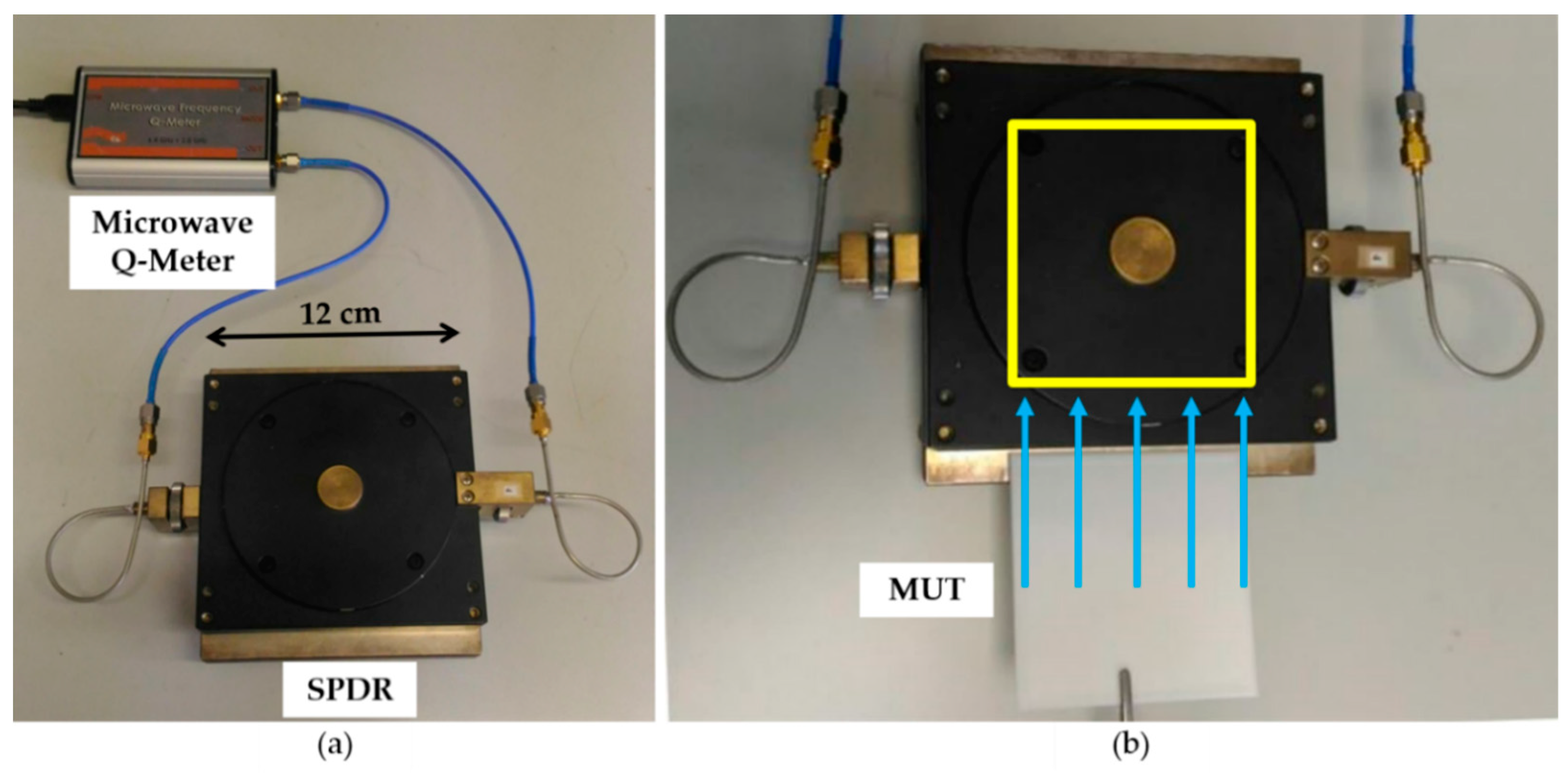
Figure 1. (a) 2.4 GHz SPDR connected to Microwave Q-Meter; (b) MUT placed into 2.4 GHz SPDR.
Designs 03 00047 g001
Figure 2. Complete SPDR measurement system.
Designs 03 00047 g002
Figure 3. X-band rectangular waveguide measurement system: (a) instrument including two waveguide halves connected to the VNA; (b) MUT inserted into the flange aperture; (c) flange with MUT inside connected to the left waveguide halve; (d) waveguide halves closed until sealed.
Designs 03 00047 g003
Figure 4. Simulated electric fields in the X-band rectangular waveguide.
Designs 03 00047 g004
Figure 5. Damaskos model 600T open resonator.
Designs 03 00047 g005
Figure 6. Damaskos model 600T open resonator with MUT in the center.
Designs 03 00047 g006
Figure 7. (a) Top view of the TE01δ mode cavity resonator; (b) MUT placed at the center in the metal cavity; (c) TE01δ mode cavity resonator closed with MUT inside.
Designs 03 00047 g007
Figure 8. TE01δ mode cavity resonator system during measurement.
Designs 03 00047 g008
Figure 9. Five printed ABS MUTs for characterization.
Designs 03 00047 g009
Figure 10. Measured (a) dielectric constant and (b) loss tangent of ABS MUTs.
Designs 03 00047 g010
Figure 11. Measured (a) dielectric constant and (b) loss tangent of PLA MUTs.
Designs 03 00047 g011
Figure 12. Measured (a) dielectric constant and (b) loss tangent of ABS and PLA MUTs at frequencies less than 20 GHz.
Designs 03 00047 g012
Table 1. The minimum size, maximum width, and thickness of MUT according to the operating frequency of SPDR [32].
Frequency (GHz)Minimum Size (mm × mm)Maximum Width (mm)Maximum Thickness (mm)
1.1120 × 1201506.0
1.970 × 701004.1
2.455 × 551003.1
Table 2. Required shape and size of MUT for measurements using SPDRs, X-band waveguide, Damaskos model 600T open resonator, and TE01δ mode cavity resonator.
MethodMUT ShapeMinimum Size
(mm × mm)
Maximum Size
(mm × mm)
Maximum Thickness
(mm)
SPDRrectangular120 × 120Any × 1506.0
SPDRrectangular70 × 70Any × 1004.1
SPDRrectangular55 × 55Any × 1003.1
X-band waveguiderectangular22.86 × 10.1622.86 × 10.16Sample-dependent
Damaskos model 600T open resonatorsquare120 × 120120 × 12050
TE01δ cavity resonatorcylinderDiameter: 6
(12 for low εr samples)
Height: 3
Diameter: 16
Height: 6
3
Table 3. Comparison of SPDR, X-band waveguide, Damaskos Model 600T open resonator, and TE01δ mode cavity resonator.
MethodClassFrequency (GHz)Calibration
Time (min)
Measurement
Time (min)
SPDRResonant perturbation1.1, 1.9, 2.4No needLess than 1
X-band waveguideTransmission/reflection8.2 to 12.43Less than 1
Damaskos model 600T open resonatorResonator10 to 7020More than 10
TE01δ cavity resonatorResonatorSample-dependentNo needLess than 1
Table 4. Printing parameters for the 3D printing of ABS and PLA samples.
MaterialInitial Layer Height (mm)Layer Height (mm)Print Temp. (°C)Bed Temp. (°C)Print Speed (mm/s)Infill (%)Infill Angle (°)Shells
ABS0.30.225011060100452
PLA0.30.22206080100452
Table 5. Measured fabricated sizes, methods, and frequencies, together with the dielectric constant and loss tangent results of the ABS MUTs.
MUTFabricated Size (mm)Measurement MethodFrequency (GHz)Dielectric ConstantLoss Tangent
ABS 1Diameter: 12.23
Height: 3.78
TE01δ mode cavity resonator16.22.490.005
ABS 222.84 × 10.15 × 1.75 X-band waveguide8.2 to 12.42.53
(mean)
0.004
(mean)
ABS 355.12 × 55.34 × 1.72SPDR2.42.310.005
ABS 470.19 × 69.88 × 1.79SPDR1.92.390.005
ABS 5120.12 × 120.34 × 1.79SPDR1.12.370.005
Open resonator12.3 to 62.62.37
(mean)
0.009
(mean)
Table 6. Measured fabricated sizes, methods, and frequencies, together with the dielectric constant and loss tangent results of the PLA MUTs.
MUTFabricated Size (mm)Measurement MethodFrequency (GHz)Dielectric ConstantLoss Tangent
PLA 1Diameter: 12.11
Height: 3.83
TE01δ mode cavity resonator16.12.510.008
PLA 222.82 × 10.12 × 1.74X-band waveguide8.2 to 12.42.52
(mean)
0.022
(mean)
PLA 355.23 × 55.11 × 1.53SPDR2.42.530.009
PLA 469.89 × 70.33 × 1.56SPDR1.92.540.008
PLA 5120.12 × 120.41 × 1.59SPDR1.12.610.009
Open resonator10.8 to 63.92.55
(mean)
0.016
(mean)