1. Introduction
Usage of white LEDs as light sources is rapidly pervading the market, with large scale marketing starting around 2010. However, the initial approach was to use these kinds of devices just as a plug-in replacement for traditional lamps, i.e., incandescent and fluorescent sources. The driving force is mainly energy savings, around 50% with respect to fluorescent lamps, and up to 80% if compared to incandescent bulbs [
1,
2].
Specific characteristics of LEDs, seen as electronic devices, opened new usage perspectives, as they are dramatically different from their predecessors. The main differences are as follows:
Quasi linear dependence of light flux from the current passing through the LED. This relationship allows for easily modulating the total emitted power just controlling the supplied current, leading to accurate light dimming in the environment. This can be used to save energy, or to improve user experience. Typical characteristics of such LED sources are described in [
3].
Reduced dimensions. White LEDs have small dimensions (1 mm × 1 mm for a 1 W source). Design of very small lamps is nowadays typical. The size reduction boundary is given by electronics size, and/or thermal considerations.
High modulation speed. White LEDs can change their flux on the nanosecond timescale, allowing for using them both to illuminate, and to carry information, given a proper modulation scheme [
4,
5].
Complex driving electronics required. The light source, typically built from several parallel strings of series connected LEDs, is typically driven by a current generator, with output voltages in the range of 10–100 V, and output currents ranging from 100mA up to several Ampere. Moreover, regulations require high power factor designs of the power supply unit if the lamp is fed by an AC line. Even in the case of DC fed lamps, power electronics are needed anyway, in order to have a fixed amount of light independent of temperature and input voltage.
Ambient Light Sensing (ALS), i.e., introducing light sensors in the environment, to collect data about illumination, and to send them to a control unit able to change the flux emitted by LED lamps, is again a typical situation in the age of Internet of Things (IoT) [
6].
The overall system is usually realized with physically separated objects. Specifically, the following devices must be introduced:
Solid state lamps, with a control input to dim them.
Light sensors, with a data output to send collected data.
A central control unit, which, according to sensed information, modulates lamps power.
A communication network, to join together these building blocks. Several solutions exist, both wired (e.g., DALI) and wireless (e.g., ZigBee).
Having separated sensors and lamps leads to a cost increase, as deployment costs are related to the number of different objects to be installed. On the other hand, integrating a light sensor inside an LED lamp is a challenge, as the high flux level of LED can easily saturate nearby photo sensors. Several topologies have been suggested to overcome this problem [
7,
8,
9], but anyway they still require to optically shield the sensor from the LEDs, and this is not practical in compact lamps. Moreover, having a light sensor inside the lamp is not sufficient to achieve luminance control, as the control system is now distributed among all the lamps, and communication is thus needed to guarantee stability of the control scheme. To better clarify this situation, we can imagine having just two lamps in a steady state, at the same power level. Now, one of the lamps could decide to decrease its power, as too much light is sensed. An adjacent lamp notices this change, and increases its power to compensate for the reduction of sensed light. Iterating this behaviour, we obtain that the first lamp will be completely turned off, and the second one will be at its maximum level, which is not the desired result. The stability of the overall control system can be achieved only by communication between lamps.
Visual Light Communication (VLC) is rapidly gaining interest too, both in indoor and outdoor environments [
10,
11,
12]. This technique uses visible light to broadcast information through free-air, from one or more lamps to other objects, but the main interest is in achieving high bandwidth efficiency, and LED lamps are mainly used only as transmitters [
13]. In addition, spread spectrum techniques are usually adopted [
5]. The main advantages of VLC are due to the absence of additional wiring, automatic confinement of information inside the room, and high bandwidth achievable on short/medium distances (typically 10–100 m). Moreover, it is a cheap solution as the light source is already available inside the lamp itself, and just the modulation circuit must be added.
In this work, instead, simplicity and cost are the driving force, in order to allow large scale deployment of ALS and VLC distributed systems fully integrated inside low cost LED lamps. In this context, high bandwidth is not a premium, as an IoT system does not need to transmit too much information (ambient light levels, temperature, people presence, etc.)
In the following, the methodology to achieve the complete design and realization of a lamp with integrated sensing and communication capabilities will be presented. The sensor is a simple light sensor, optimized to perform correct measurements nearby high power LED light sources. The VLC system is based on modulation of the light emitted by the lamp itself, in order to implement transmission function. On the other hand, the light sensor, used to measure ambient light, is used to implement the receiver of the communication system, through adequate conditioning and filtering. The implemented communication system is a general purpose anyway and can be used to transmit even different informations, if needed, such as lamp state, lamp life informations, temperatures, etc.
2. Materials and Methods
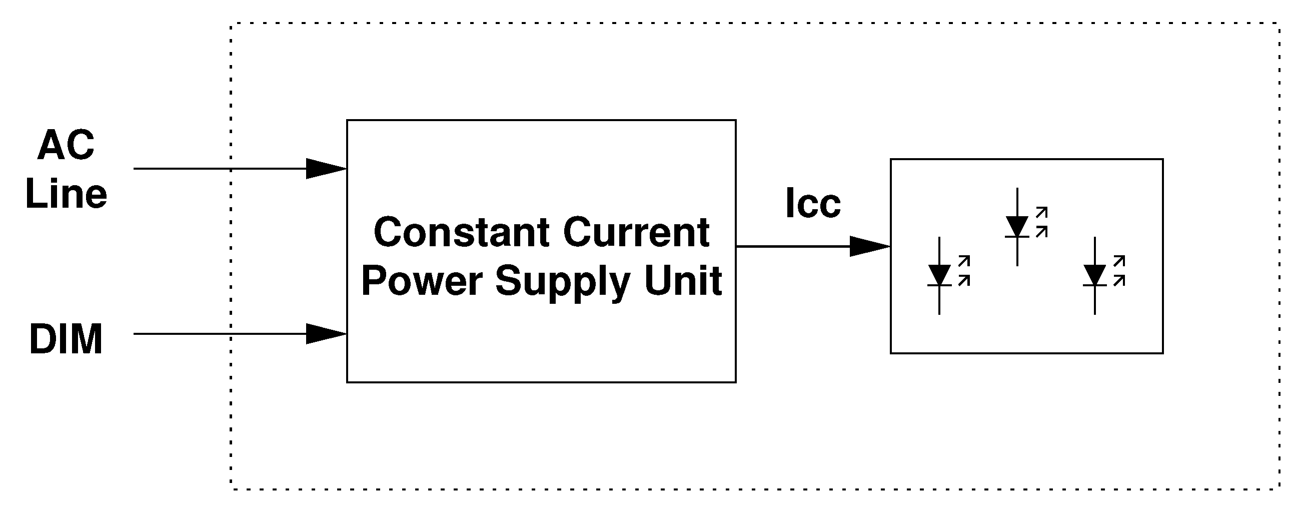
In a typical solid state lamp, represented in
Figure 1, a Power Supply Unit (PSU) convert the AC line voltage to a DC constant current. Usually, this current is not perfectly constant, and it is slightly modulated at two times the AC line frequency, in order to satisfy High Power Factor (HPF) requirements. A single stage Power Factor Correction (PFC) is used, in order to minimize PSU cost in low power LED lamps (1–50 W). At higher power levels, a two stage power supply can be used, in order to reduce light flickering. The first stage is a PFC, and the second one is constant output current DC/DC converter. LEDs are then directly fed by the PSU. Finally, the PSU, if dimmable, has a control input (DIM), used to change the amount of light emitted by the lamp. Several standards exist to control lamp power, like DALI, 0–10 V analog control, or variable duty cycle PWM.
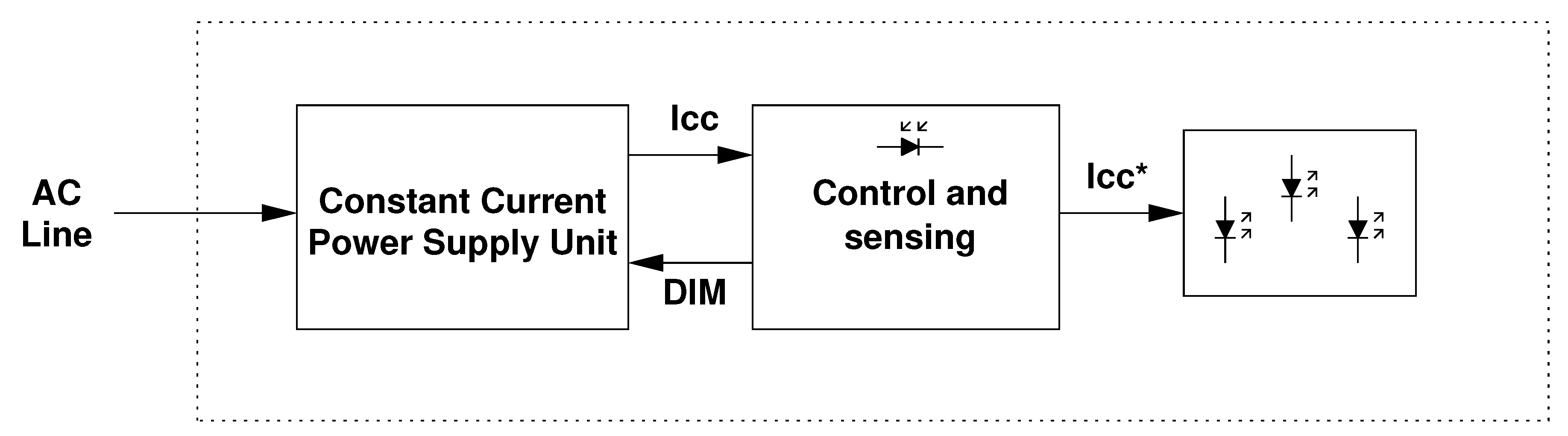
The aim of this work is to design a block that could be easily customized to a variety of lamps, different for power, size, and shape. From this point of view, it is mandatory to have a circuit with minimal complexity, but capable of operating in a broad range of operating conditions too. In the proposed solution (
Figure 2), a control and sensing unit are interposed between the PSU and the LEDs. This block has the task to allow accurate Ambient Light Sensing (ALS), and, at the same time, to modulate emitted light in such a way to allow Visual Light Communication (VLC). The light sensor is a photodiode, which act both as a sensor for ambient light and as a receiver for optical signals coming from other lamps. The photodiode has an integrated optical filter, in order to resemble human eye responsivity. This does not compromise receiver sensitivity, as typical white LEDs have good emission in the green region of visible spectrum, where a photodiode filter has good responsivity too.
To accomplish these functions, at each cycle of the AC line input, the LEDs are turned off for a short interval (a negligible fraction of the cycle time). This interval is centered around the zero crossing of the sinusoidal input waveform. The usage of the AC line as a time reference gives best results, as it allows automatic synchronization of every lamp connected to the same power connection. Moreover, performing measurement and communication activities at a time in which the power line is crossing zero minimizes errors due to interferences, both originated by the internal PSU, and injected from the outside.
Following LEDs being turned off, a short amount of time must elapse, in order to accomplish a photo detector and amplifier settling time. Now, a sequence of samples is gathered and stored for further calculations. If no communication is needed, the average value of these samples represents the sensed ambient light level.
If communication is needed, instead, a modulation scheme must be introduced. The chosen approach is based on the emission of few pulses by the LEDs, injecting a controlled current. Zeros and ones are represented by a different number of pulses at different frequencies. A key point is that the total energy must not change, in order to avoid visible luminance changes of the lamp as a function of the transmitted pattern. As an example, the two different modulations can be four pulses at 100 kHz, and eight pulses at 200 kHz to represent ‘0’ and ‘1’, respectively (
Figure 3).
Frequency of pulses is critical, as it must be high enough to require a short LED off time. Otherwise, LED turn-off could cause a visible or anyway annoying flicker effect. Using frequencies in the range of hundredths of kHz satisfies this requirement.
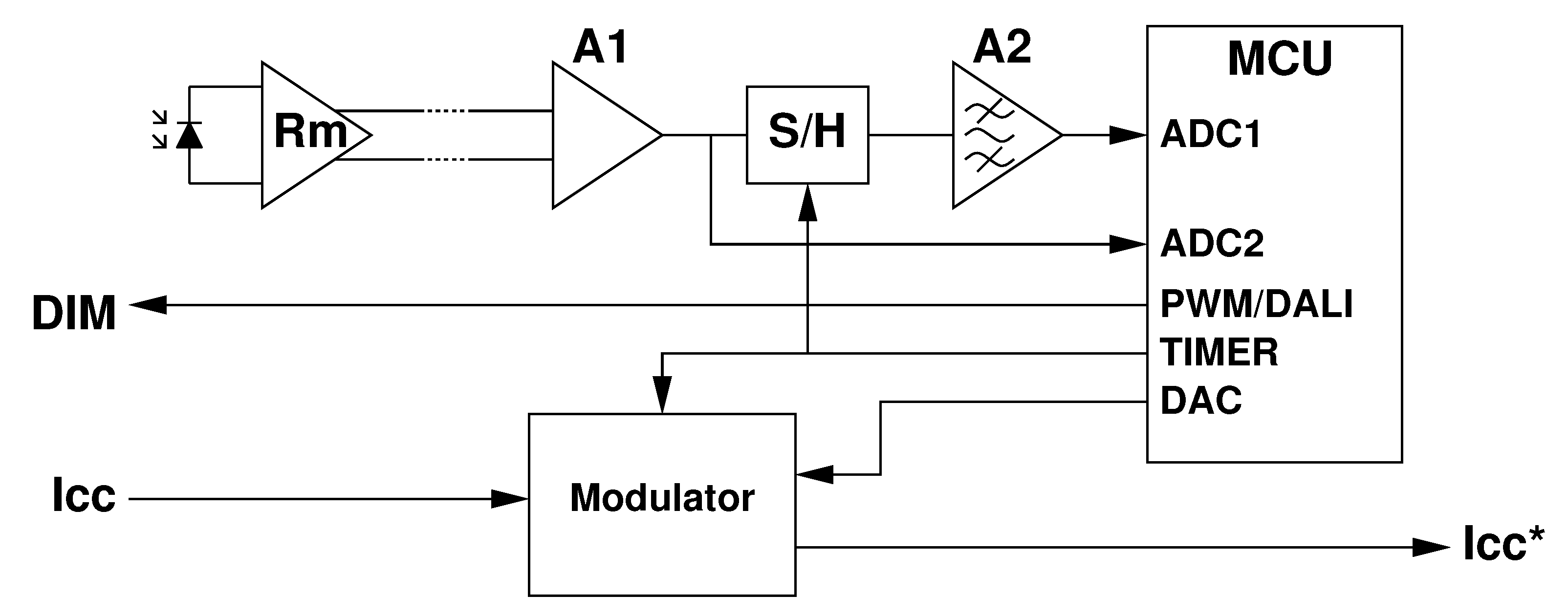
The internal structure of the circuit designed to implement the above functionalities is depicted in
Figure 4.
A photodiode, with spectral response resembling the human eye one, feeds a transresistance amplifier. It has a differential output, as it must be mounted on the front of the lamp, near the LEDs, and the noise level along the cables can be quite high. The lamp PSU itself has nodes swinging from 0 to 700 V at 20–200 kHz, generating significant EMI. In addition, the gain of the transresistence amplifier is limited, as it must not saturate even when the LEDs are turned on. It means that the signal measured when LEDs are turned off has limited amplitude, and a single ended approach would degrade precision and reliability. Using rail-to-rail amplifiers, the relationship among maximum transresistence, power supply, photodiode sensitivity and maximum illuminance is given by the following equation:
where
is the maximum allowable transresistance gain,
is the power supply voltage,
is the maximum illuminance level seen by the photodiode, and
is photodiode sensitivity. Typical low-cost photodiode sensitivity for a 0805 device is 0.4 nA/lx, and the LED source adjacent to the photodiode itself can generate up to 100,000 lx. Maximum transresistance gain, using rail-to-rail amplifiers with 5 V power supply, is then about 100 k
. On the other hand, when measuring ambient light with the above calculated transimpedance gain, illuminance is between 10 lx and 1000 lx, thus generating output signals between 0.4 mV and 40 mV. Anyway, no further gain is allowed, to avoid output saturation, even using a fast recovery amplifier. In fact, even if relevant measurements are performed only when LEDs are off, a saturation of the transimpedance amplifier would cause charge accumulation inside the photodiode, and recovery from this state would be very slow.
To overcome this limitation, the differential signal is fed to an instrumentation amplifier (A1), used to eliminate common mode noise, and then sent to a sample-and-hold. This one is in hold mode when LEDs are turned on, and in sample mode when they are turned off. Its task is to minimize transients at the input of the successive stages, allowing an easier design (and higher gain) of the following band-pass filter A2. In fact, an abrupt change at the input of the filter (fall down of the LED power—see
Figure 3) would be amplified anyway, and must be avoided. A2 is introduced to further improve SNR, and to increase sensitivity.
The outputs of A1 and A2 are sent to a microcontroller (MCU), which samples the signals while LEDs are off, and store them for further computations. Digital signal processing algorithms, described in the following, are executed while LEDs are on, in the remaining portion of the AC line cycle.
Two different calculations must be performed:
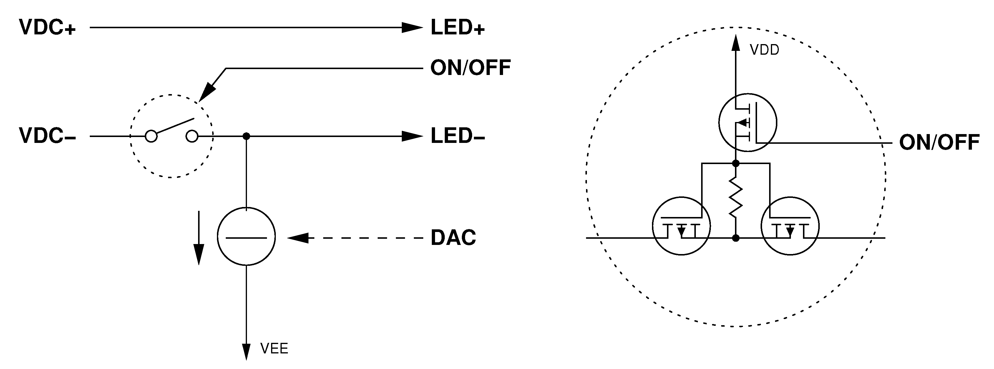
Light modulation is implemented by the modulator block of
Figure 4. It transforms the constant current
, fed by the PSU, into
, sent to the LEDs. A simplified schematic is visible in
Figure 5. It is basically a switch, used to interrupt the current flow from the lamp PSU, and a current generator, driven by the DAC output of the MCU. The current generator is implemented through a current mirror with gain. The gain is needed as LEDs driving current are typically two orders of magnitude greater than the output current capabilities of the DAC. The switch is implemented through a pair of source coupled NMOS transistors. This topology cancels the presence of the body diodes, allowing for blocking current flow in both directions when switch MOSFETs are both turned off. (right side of the figure).
3. Results
A physical implementation has been designed, using off-the-shelf discrete components, and simulated, taking in account parasitics. The circuit has been designed in the hypothesis to insert it inside a T8 form factor LED tube. Special care has been taken to reduce overall cost, obtaining a module which costs less than 10 USD.
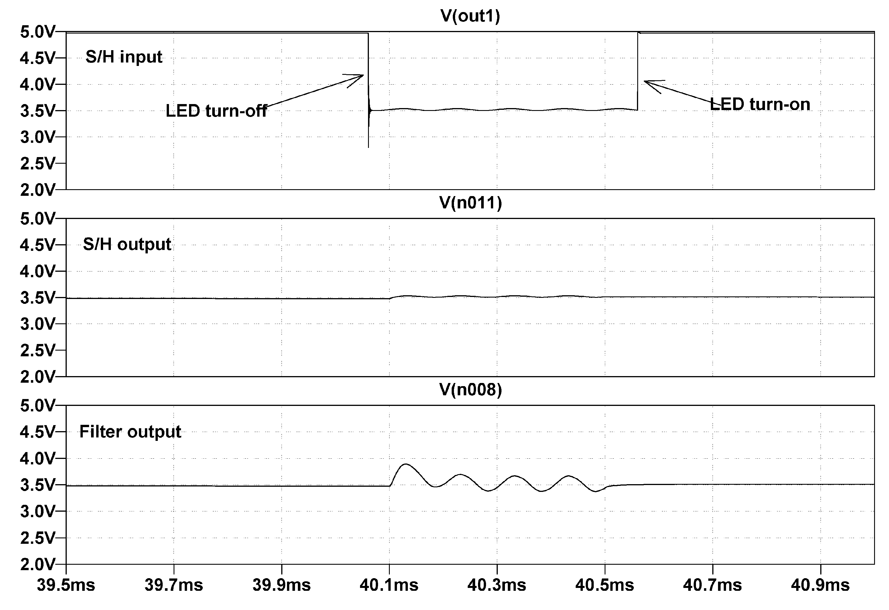
In
Figure 6, results obtained from LTSpice simulator are shown. In particular, relevant waveforms of the ALS and VLC blocks are shown. The upper waveform (
) is the signal at the input of the S/H, showing wide transitions at LED turn-off and turn-on. Even if not clearly visible, when LEDs that are off a VLC signal is superimposed to the background light level, with an amplitude of 32 nA, corresponding to an 80 lx luminance variation on the photodiode. The center one (
) is the output of the S/H, showing almost complete cancellation transients. Finally, the bottom waveform (
) is the modulated signal at the output of the band-pass filter, sent to the input of the A/D converter into the MCU, to be processed by the two Goertzel digital filters.
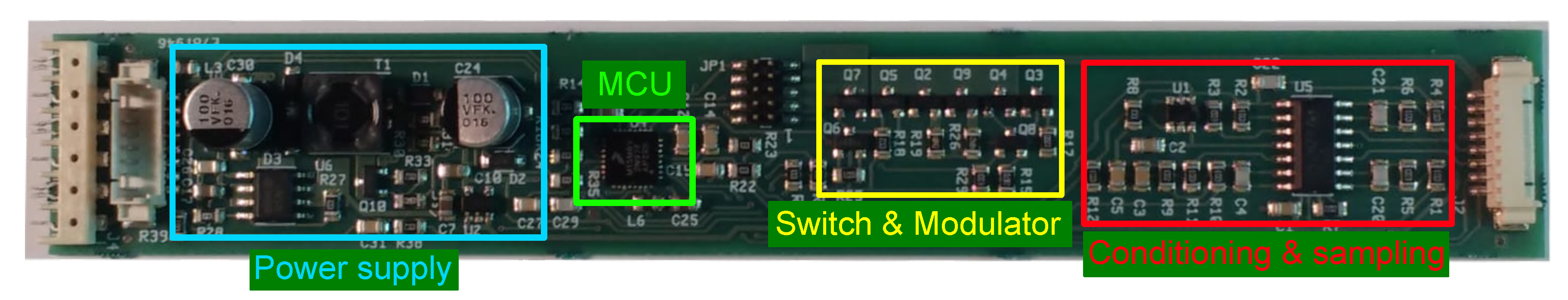
The board has been then built, and its final layout is depicted in
Figure 7. Coloured rectangles identify the main building blocks of the realized architecture. From left to right, they are:
Blue frame: power supply of the board. To accomplish the usage inside a variety of different lamps, a simple linear regulator has been designed, to generate 5 V and 3.3 V from the unregulated DC input supply rail. Moreover, a flyback is introduced to generate the VEE rail (currently at −12 V), used to feed the modulator circuit. The latter is directly driven by a PWM generated from the microcontroller. This way, it can be turned off as needed, for example to minimize noise during a receiver sampling phase.
Green frame: microcontroller unit. A 48 MHz low power ARM is used, in order to have enough computing power for data processing (digital filters). The implemented program includes both VLC and automatic dimming based on ALS. The actual code footprint is 16 kB of code and 2 kB of data, leaving space for introduction of further functionalities in the future.
Yellow frame: power switch and modulator. The switch is built up of low power MOSFETs, maximizing power efficiency. The modulator is a current mirror, with BJTs as active elements. They are used for the good precision achievable at low cost in a discrete design.
Red frame: signal conditioning and sampling. A quadruple operational amplifier is used to implement the circuitry described in the preceding sections. A discrete low resistance, low leakage current switch is used to build up the S/H function.
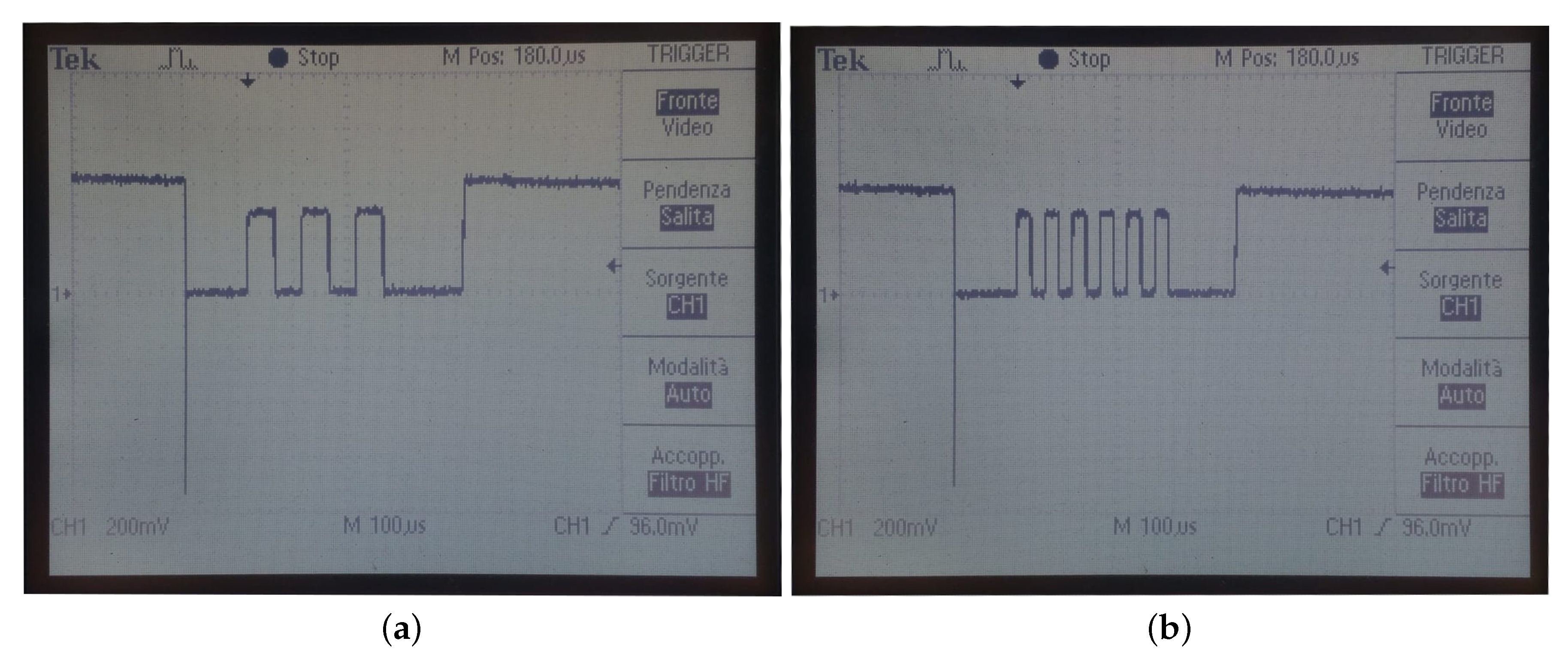
Measurements have been performed in a real environment, inserting the control board in an LED T8 tube, fed by 230 V AC line. In the following
Figure 8, the currents fed to the LED string in the case of ‘0’ and ‘1’ transmission are shown, as required by the transmission protocol described above. Three pulses are used for ‘0’, and 6 for ‘1’. The action of the power switch which turns off and on the LED light is also visible just before and after modulation pulses. ALS sampling is performed when LED is off, of course. The slight misalignment in LED current on the left and right sides of the image is correct, as light current is modulated at 100 Hz by the PFC to achieve near-unity power factor (0.99 at 10 W in this case).
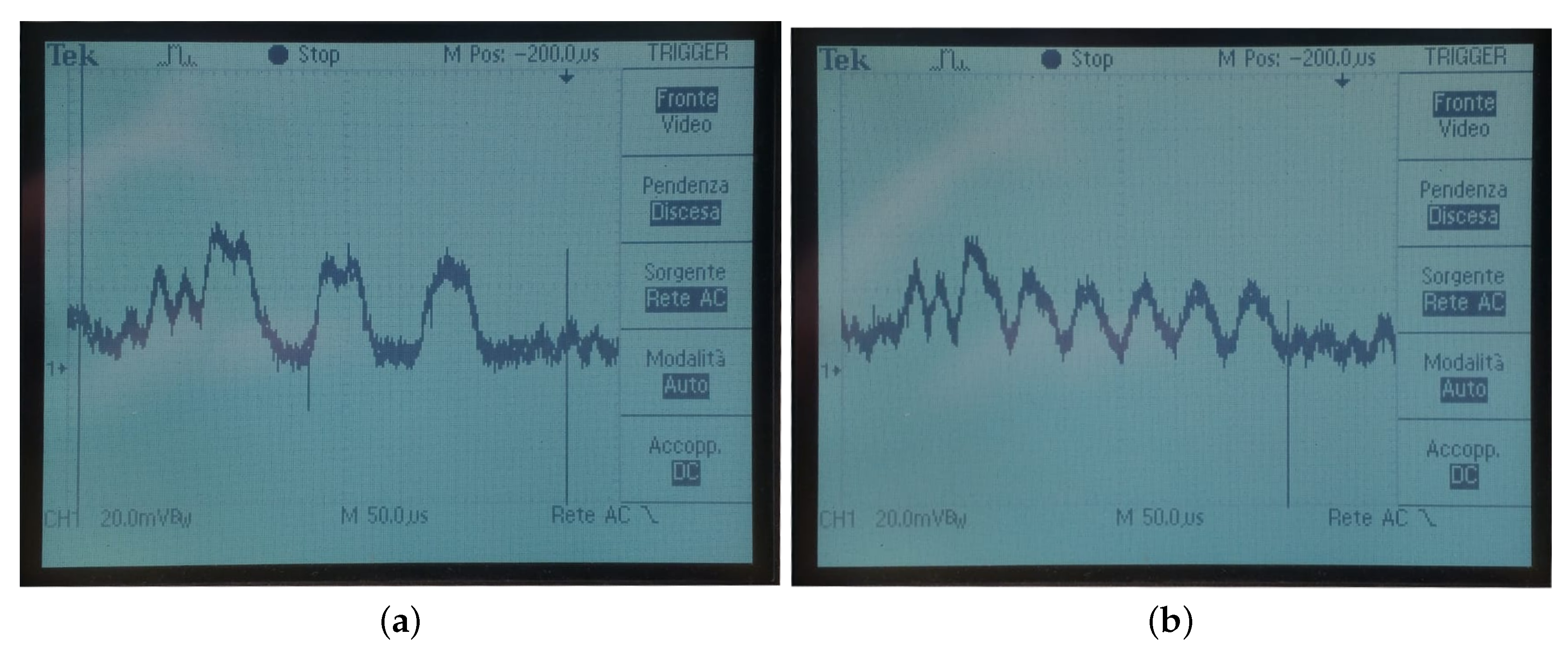
The measurements at the receiving side are instead visible in
Figure 9. Due to the strong signal attenuation related to distance between the transmitting and the receiving lamps, only the processed signals just at the input of the microcontroller can be shown, after preamplification, noise cancelling, sampling and filtering. These signals will be then further digitally processed by the microcontroller. On the left, the signal corresponding to a ‘0’ is shown (three pulses), while, on the opposite side, a ‘1’ is received (six pulses at doubled frequency). As it can be easily seen, the signal is clearly emerging from the noise, even if at reduced voltage levels (20 mV
). This is a considerable result, given that, at about 5 cm, and, without any kind of shield, there are nodes switching at 600 V
, 100 kHz. The equivalent light input signal is about 1 lx.
4. Conclusions
In this work, a methodology to allow simultaneous Ambient Light Sensing and Visual Light Communication inside a simple LED lamp has been presented. It is applicable independently of lamp power and type, given it was possible to interpose the designed module between the PSU and the LEDs itself. A practical implementation has been realized, in order to be inserted in standard T8 LED tubes to demonstrate of solution feasibility, even in small spaces. The current solution is able to transmit 100 or 120 bit/s, depending on the frequency of main lines. Communication distance depends directly from the power of lamps, leading to a sort of autoscaling of the system. In fact, a large room requires more powerful light sources, i.e., greater communication range too. In fact, no other similar solution, directly integrating light sensors near the light sources, is known, giving to our solution big advantages from the point of view of installation cost reduction and flexibility. A further improvement could be the introduction of more sophisticated modulation techniques, in order to increase bandwidth and reliability of communication. Moreover, it is possible to imagine the integration of other kinds of sensors (temperature, humidity, quality of air, etc.) and to use the communication capabilities of lamps to broadcast collected information.


