Article

Analysis of an H∞ Robust Control for a Three-Phase Voltage Source Inverter

by
Muhammad Ahmad Usman Rasool
*,
Muhammad Mansoor Khan
,
Zahoor Ahmed
and
Muhammad Abid Saeed
School of Electronic Information and Electrical Engineering (SEIEE), Shanghai Jiao Tong University, Shanghai 200240, China
*
Author to whom correspondence should be addressed.
Inventions 2019, 4(1), 18; https://doi.org/10.3390/inventions4010018
Submission received: 30 December 2018 / Revised: 20 February 2019 / Accepted: 27 February 2019 / Published: 12 March 2019

Abstract

:
Recently, power quality improvement has gained a lot of attention due to the rapidly increasing use of power electronics equipment. Several control strategies for DC/AC Voltage Source Inverters (VSI) have been developed to obtain good quality output with low harmonic distortion. This paper proposes a robust control scheme to improve the power quality of a three-phase DC/AC VSI. The control scheme includes an outer voltage loop and an inner current loop, with both controllers designed by the standard H∞ robust control technique. The system with the proposed controller has a low total harmonic distortion (THD) and improved power quality of output voltage in the presence of linear and non-linear loads. The simulation is carried out in MATLAB/Simulink environment, and the results of the proposed control scheme are compared with the performance of dead-beat (DB) predictive control and conventional proportional integral (PI) control. It is observed from the results that the proposed control scheme outperforms other control schemes in terms of the THD level, having a better steady-state and transient performance.

1. Introduction

Voltage Source Inverters (VSI) produce sinusoidal waveforms and unity power factor resulting in a feasible solution for distributed power generation [1]. A Distributed Power Generation System (DPGS) is a system typically based on renewable energy resources (RES), power electronics, loads, and intermediate energy resource units [2]. However, high-frequency switched voltages are generated because of the Pulse Width Modulation (PWM) of VSI which results in the distortion of output voltage and load currents [3]. Generally, these distortions are removed by using a filter which is integrated at the output of the inverter system. The control strategies for the inverter systems are established to guarantee the maximum quality of the control parameters, which can lead researchers to have a great interest in improving these strategies.
In a literature survey, several control techniques have been applied to a converter system which includes, proportional-integral (PI) control [4,5], H∞ control [6,7,8], sliding mode control (SMC) [9,10], adaptive control [11,12] repetitive control [13,14], model predictive control (MPC) [15,16], and dead-beat (DB) control [17,18]. In reference [4], PI control is easier to implement, but since it requires proper gain tuning, it is hard to optimize the closed-loop performance of the system. Moreover, under the non-linear condition the total harmonic distortion (THD) value of the output voltage is not low. In another study [7], a loop-shaping control strategy using the H∞ control scheme is investigated on a single-phase inverter which possesses a simple structure and is also robust against the model uncertainties, whereas this control technique only ensures local stability. In references [9,10], the SMC and adaptive control [11] are robust to load disturbance, but due to the switching structure of the system, a chattering problem is produced which can reduce the output performance of the system, while the adaptive control has the computational complexity. In reference [13], a repetitive control method is applied on a three-phase UPS system in order to deal with fluctuating loads and parameters variations and to achieve high-quality sinusoidal output voltage, whereas in the case of computation and gain selection, this method becomes complicated and has a slow response time. To model the three-phase inverter with a DB controller, various studies have been carried out. For instance, the conventional DB control technique in reference [17] is found to be robust and have a rapid response; however, it is highly sensitive to disturbances, parameters mismatching, and steady-state error. For current control, a novel adaptive self-tuning technique based on DB control has been proposed for a three-phase PWM voltage source inverter in a study [18]. In reference [15], MPC has a simple structure and a good performance but it needs an accurate model of the converter system, which makes it highly sensitive to model uncertainties and parameter mismatching. In reference [16], the MPC technique is discussed for a three-phase VSI with an output LC filter. The proposed technique is found to be robust and has the ability to handle several disturbances. The cost function in the system is also found to be adequate to obtain the minimal voltage error. However, the MPC method needs to calculate a cost function for seven possible switching vectors to select an optimum one. These calculations impose a high computational burden. Over the past few years, the H∞ robust control theory has also received great attention in the field of control, and its applicability has been reported to some extent. H∞ robust control is quite a handy tool, especially when it comes to the robustness of the closed-loop system. The H∞ control systems are monolithic, where embedded control systems are decentralized collections of simple control elements.
This paper addresses the design of a robust control scheme for a three-phase DC/AC VSI. The main aim is to improve the power quality of output voltage having a low THD value in the presence of linear and non-linear loads. This control strategy comprises an outer voltage and an inner current control loop designed by using standard H∞ control formulation. While designing a controller, the selection of weighting function and weighting parameters plays an important role, as the suitable weighting function results in the controller having an improved system response. In order to demonstrate improvements, the proposed controller is compared with a DB predictive and a PI controller. The simulation results under linear and non-linear loads are presented using MATLAB/Simulink environment, verifying the feasibility and good performance of the proposed control strategy.

2. Proposed Control Scheme

In this section the design of H∞ robust control is discussed [18]. The schematic diagram of the system with the controller is shown in Figure 1.
The H∞ control theory is an effective method of designing a controller to guarantee the performance of the system under worst case disturbance. The key objective of the H∞ controller is to keep a clean and balanced output voltage in the presence of linear and non-linear loads. The general description of a standard feedback robust control system structure is shown in Figure 2a, where P ( s ) is the generalized system, and F ( s ) is the controller model. The transfer function from the input w to the output z is denoted by T z w . Here, it should be noted that the block diagram shown in Figure 2a is fairly general. The signal w can include both reference and disturbance signals. P ( s ) can include both the plant and the disturbance model. Moreover, the uncertainties can also be included in P ( s ) . The main idea of the robust control is to separate the known part and the unknown part from the knowledge about the uncertain system under investigation.

3. State Space Model of the Augmented Plant

As depicted in Figure 3, the system consists of an inverter, an LC filter, and a PWM generator. The series winding resistance R f and damping resistance R d are also included in the filter circuit to decrease the ringing effect. The inverter and PWM are modelled by using an average voltage approach with the limits of the DC-link voltage [19]. Over one cycle period, the average value of u f is equal to u c . So, the inverter parameters and PWM blocks are neglected while deriving the plant transfer function. The inductor current and capacitor voltage are chosen as state variables x = [ i L u c ] T . The external input w = [ i 2 u r e f ] T consists of the load current i 2 and the reference voltage u r e f , as shown in Figure 2b; the control input is denoted as u . The output signal from the plant P is the tracking error e = u r e f u o , which is the difference between the reference voltage and the output voltage. The state space description of the plant P is given as follows:
x ˙ = A x + [ B 1 B 2 ] [ w u ] ,   , y = C 1 x + [ D 1 D 2 ] [ w u ]
x ˙ = A x + B 1 w + B 2 u
y = C 1 x + D 1 w + D 2 u
A = [ R f + R d L f 1 L f 1 C f 0 ] ; B 1 = [ 1 L f 0 1 C f 0 ] ; B 2 = [ 1 L f 0 ] ; C 1 = [ R d 1 ] ; D 1 = [ R d 1 ] ; D 2 = [ 0 ]
The corresponding transfer function of the plant becomes P = [ D 1 D 2 ] + C 1 ( s I A ) 1 [ B 1 B 2 ] . In the results, the following matrix is used:
P = [ A B 1 B 2 C 1 D 1 D 2 ]

4. Formulation of the Standard H∞ Control Problem

To assure the system stability, an H∞ control problem is formulated for the voltage loop, as shown in Figure 4. In order to minimize the H∞ norm, Figure 4 is proposed for the transfer function T z ˜ w ˜ = K ( P ˜ , C ) from w ˜ = [ v w ] T to z ˜ = [ z 1 z 2 ] T , after opening the feedback loop, and the weighting parameters ξ and μ are introduced. The closed loop system can be realized as:
[ z ˜ y ˜ ] = P [ w ˜ u ] ; u = C y ˜
Here, P ˜ is the extended plant, and C is the controller to be designed. The extended plant P ˜ consists of the original plant P together with the low-pass filter W L and the weighting parameter ξ and μ , which are added to provide freedom in designing the controller. The weighting parameter ξ is added to adjust the relative importance of v with respect to w , and another weighting parameter μ is added to adjust the relative importance of u with respect to z 1 . The parameters ξ and μ also play an important role in order to guarantee system stability; these parameters are selected on the basis of the procedure provided in reference [18].
The weighted function W L u is realized as:
W L u = [ A L u B L u C L u D L u ] = [ ω c ω c 1 0 ]
y ˜ = e + ξ u v = ξ u v + [ A B 1 B 2 C 1 D 1 D 2 ] [ w u ]
y ˜ = [ A 0 B 1 B 2 C 1 ξ u D 1 D 2 ] [ v w u ]
z 1 = W L u y ˜
z 1 = [ A L u B L u C L u D L u ] [ A 0 B 1 B 2 C 1 ξ u D 1 D 2 ] [ v w u ]
z 1 = [ A 0 0 B 1 B 2 B L u C 1 A L u B L u ξ u B L u D 1 B L u D 2 0 C L u 0 0 0 ]
z 2 = μ u u
The extended plant can be realized as follows:
P ˜ u = [ A 0 0 B 1 B 2 B L u C 1 A L u B L u ξ u B L u D 1 B L u D 2 0 B L u 0 0 0 0 0 0 0 μ u C 1 0 ξ u D 1 D 2 ]
The controller C u can then be found according to the extended plant P ˜ u using the H∞ control theory problem, e.g. using the function hinfsyn provided in MATLAB®.

5. Design Example

As an example, the controller will be designed in this section for a simulation setup on the MATLAB/Simulink software package with the system parameters given in Table 1.

5.1. Design of H∞ Current Controller

The inner current loop should be designed such that it has a high bandwidth in order to get better disturbance rejection capability. For this purpose, while designing the H∞ current controller, the weighting function was chosen as W L i = 20 × 314 2 s 2 + 50 s + 314 2 , and the weighting parameters were selected as ξ i = 100 and μ i = 2.5 . Finally, by defining the inputs and outputs of the augmented plant using the linear analysis tool and applying the hinfsyn function on MATLAB, the H∞ current controller C i was obtained as:
C i = 9.694 s 9 + 6.039 s 8 + 1.035 × 10 13 s 7 3.619 × 10 16 s 6 1.981 × 10 21 s 5 1.49 × 10 24 s 4 + 1.275 × 10 29 s 3 1.8 × 10 31 s 2 + 1.138 × 10 34 s 2.39 × 10 36 s 10 + 2.463 × 10 5 s 9 + 6.642 × 10 10 s 8 + 6.576 × 10 15 s 7 + 2.528 × 10 20 s 6 + 4.174 × 10 24 s 5 + 2.524 × 10 28 s 4 + 3.308 × 10 30 s 3 + 4.99 × 10 33 s 2 + 2.846 × 10 35 s + 2.408 × 10 38
Using the reduced-order model approximation technique [20] on MATLAB, the controller is reduced to second order without causing any noticeable performance degradation, after canceling the poles and zeros that are close to each other. The bode plots of the original and reduced H∞ current controllers are shown in Figure 5b.
C i = 9.403 × 10 4 s 2 5.315 s + 978.9 s 2 + 49.99 s + 9.862 × 10 4

5.2. Design of the H∞ Voltage Controller

For designing the H∞ voltage controller, the weighting function W L u was chosen as W L u = 314 2 s 2 + 50 s + 314 2 for 50 Hz, and the weighting parameters were selected as ξ u = 100 and μ u = 2.5 . For the system parameters of the plant, the H∞ voltage controller C u was obtained, which nearly minimized the H∞ norm of the transfer function w ˜ u to z ˜ u , using the hinfsyn function as:
C i = 1.025 × 10 6 s 9 + 9.433 × 10 10 s 8 + 3.531 × 10 15 s 7 + 6.294 × 10 19 s 6 + 7.678 × 10 23 s 5 + 4.851 × 10 27 s 4 + 1.566 × 10 31 s 3 + 1.022 × 10 34 s 2 + 1.962 × 10 36 s + 8.856 × 10 38 s 10 + 2.463 × 10 5 s 9 + 6.642 × 10 10 s 8 + 6.576 × 10 15 s 7 + 2.528 × 10 20 s 6 + 4.174 × 10 24 s 5 + 2.524 × 10 28 s 4 + 3.308 × 10 30 s 3 + 4.99 × 10 33 s 2 + 2.846 × 10 35 s + 2.408 × 10 38
Using the reduced-order model approximation technique [20] on MATLAB, the controller is reduced to second order without causing noticeable performance degradation, after canceling the poles and zeros that are close to each other. The bode plot of original and reduced H∞ voltage controller is shown in Figure 5a.
C i = 9.812 × 10 2 s 2 + 557.4 s + 3.627 × 10 5 s 2 + 49.99 s + 9.862 × 10 4

5.3. Design of PI and DB Predictive Control Schemes

In the literature, several analytical methods have been proposed to design a PI controller; however, in this case, the gains of PI voltage and current controllers are calculated using the method described in reference [5]. After calculating the PI values for voltage and current loop, the gains are optimized using trial and error for the optimum design of a PI controller. Table 2 shows the values of gain selected for the optimum design of PI and DB predictive controllers.
The design of the DB predictive controller consists of an inner current loop and an outer voltage loop designed by the DB predictive control scheme described in references [21,22]. However, for an optimum design and precise voltage control, a disturbance observer and a state estimator have been incorporated into the system. The final equation of the DB control law which is used to generate reference signals for PWM is given as:
u r , r e f ( k ) = u c ( k + 1 ) + L T s [ i L , r e f ( k ) i L ( k ) ]
Here, u r , r e f is the reference voltage, L is the filter inductance, T s is the sampling time, i L , r e f is the current control loop reference value, and i L is the output value of current control loop. Also, the equations of the state estimator (19) and disturbance observer (20) are given as follows:
x ˜ ˙ d = ( A M L M C M ) x ˜ d + B M d ˜ x ˜ ˙ d = A H x ˜ d + B M d ˜
d ˜ ˙ = η C M A M x ˜ d C M B M d ˜
Here, x ^ d is the estimated system states, d ^ is the estimated disturbances, L M is the Luenburger gain matrix, and the observer gain is η. The Equations (19) and (20) can be combined to form a matrix given as:
[ x ˜ ˙ d d ˜ ˙ ] = [ A H B M η C M A M η C M B M ] [ x ˜ d d ˜ ]
w ˜ ˙ = K w ˜
The tuning parameters are selected such that matrix K should be Hurwitz, i.e. all closed-loop poles are on the left half plane [23]. After some trial and error, the parameters for the Luenburger gain matrix L M and observer η gain were selected as L M = [ 5.3519 1.0460 ] T and η = 0.1 , respectively.

6. Simulation Results

The evaluation of the proposed controller was made in stand-alone mode with linear and non-linear loads. The control strategy was evaluated in three situations: (i) steady-state response with linear (ii) steady-state response with non-linear loads and (iii) transient response with linear load. In order to demonstrate improvements in the results, the proposed controller was compared with a DB predictive controller and a PI controller.

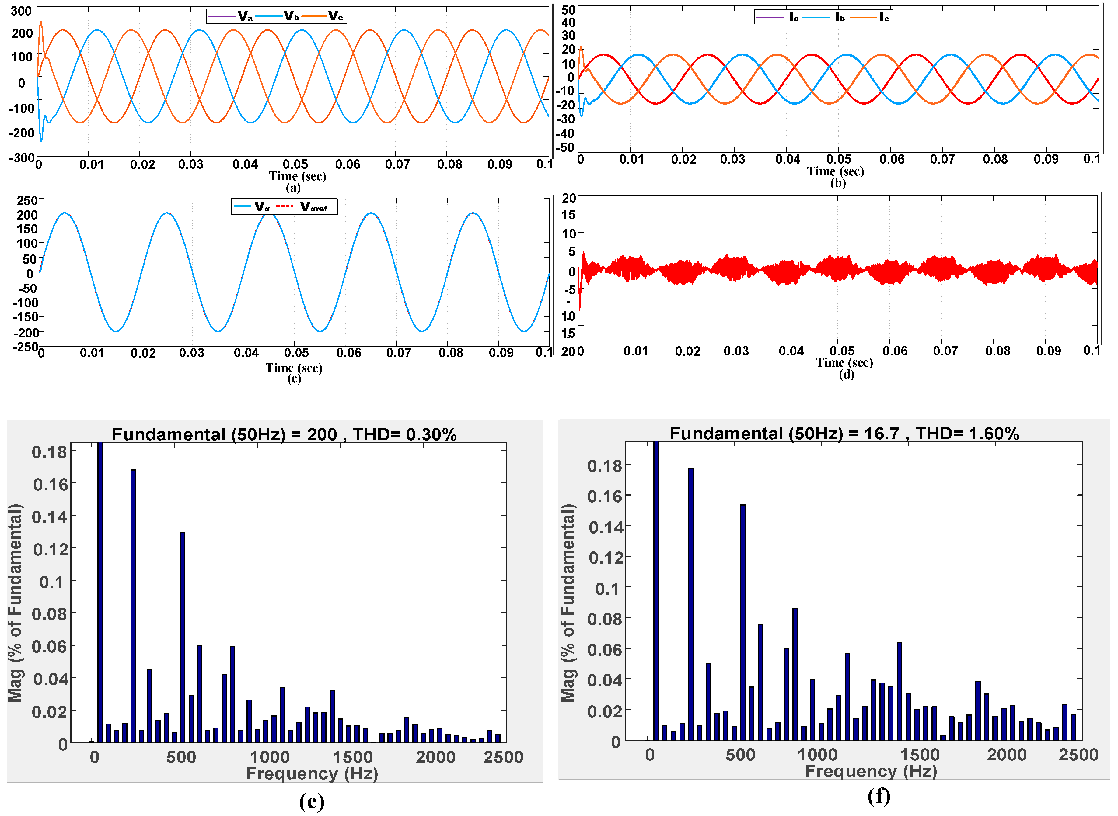
6.1. Steady-State Performance in Stand-Alone Mode

In this section, the steady-state performance of the system with the aforementioned controller is discussed in detail. The evaluation of the controller was made for a resistive load, i.e. R a = R b = R c = 12   Ω , and a non-linear load (uncontrolled rectifier loaded with an LC filter L = 150   mH ,   C = 1000   µ F , and a resistor R = 20   Ω ).

6.1.1. Steady-State Performance with a Resistive Load

The waveform of the output voltage v a , v b , v c , the load current i a , i b , i c , and the THD graph for H∞ robust controller, DB predictive controller, and PI controller with linear resistive loads in steady-state condition are shown in the Figure 6, Figure 7 and Figure 8, respectively. The THD values of voltage and current with linear resistive loads are also given in Table 3. As can be seen from Table 3, in the case of linear resistive load, the output voltage THD for H∞ robust control was recorded as 0.30%, whereas the THD value of the output voltage in the case of the DB predictive controller was 0.60%, and for the PI controller, it was 0.4%. The reference value for attaining the static response was set to 200 V, and the resistive load was taken as 12 Ω. It can be observed from Figure 8a that, in the case of the PI controller, the system starts with fluctuations and achieves the reference value within 50 ms. In contrast, while taking the static response for the H∞ robust controller and DB predictive controller as depicted in Figure 6a and Figure 7a, the system starts without any large fluctuation or perturbation and achieves the referred value rapidly. The simulation results show that the system has a smooth output voltage and current waveforms which depict its satisfactory performance with linear resistive loads in steady-state condition.

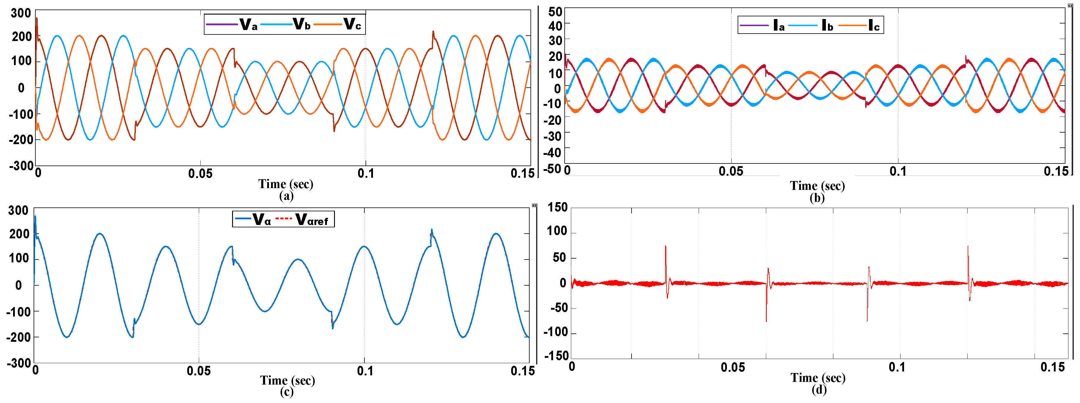
6.1.2. Steady-State Performance with Non-Linear Load

The waveforms of output voltage v a , v b , v c , the load current i a , i b , i c , and the THD graphs with the H∞ robust controller, DB predictive controller, and PI controller are shown in Figure 9, Figure 10 and Figure 11, respectively. The THD values of voltage and current with non-linear loads are also given in Table 4. As can be seen from Table 4, in the case of non-linear loads, the output voltage THD for the H∞ robust controller was recorded as 3.06%, whereas the THD value of output voltage in the case of the DB predictive controller was 4.54%, and for the PI controller THD was 4.7%. The reference value for attaining the static response was set to 200 V, and a non-linear load uncontrolled rectified loaded with LC filter L = 150   m H ,   C = 1000   μ F , and a resistor R = 20   Ω was considered. It can be observed from Figure 9a that with the H∞ robust controller, the system has fewer fluctuations than with the DB predictive controller and the PI controller, as depicted in Figure 10a and Figure 11a, in the case of non-linear uncontrolled rectified load. The simulation results showed that the H∞ robust controller performs better with non-linear loads in steady-state condition.

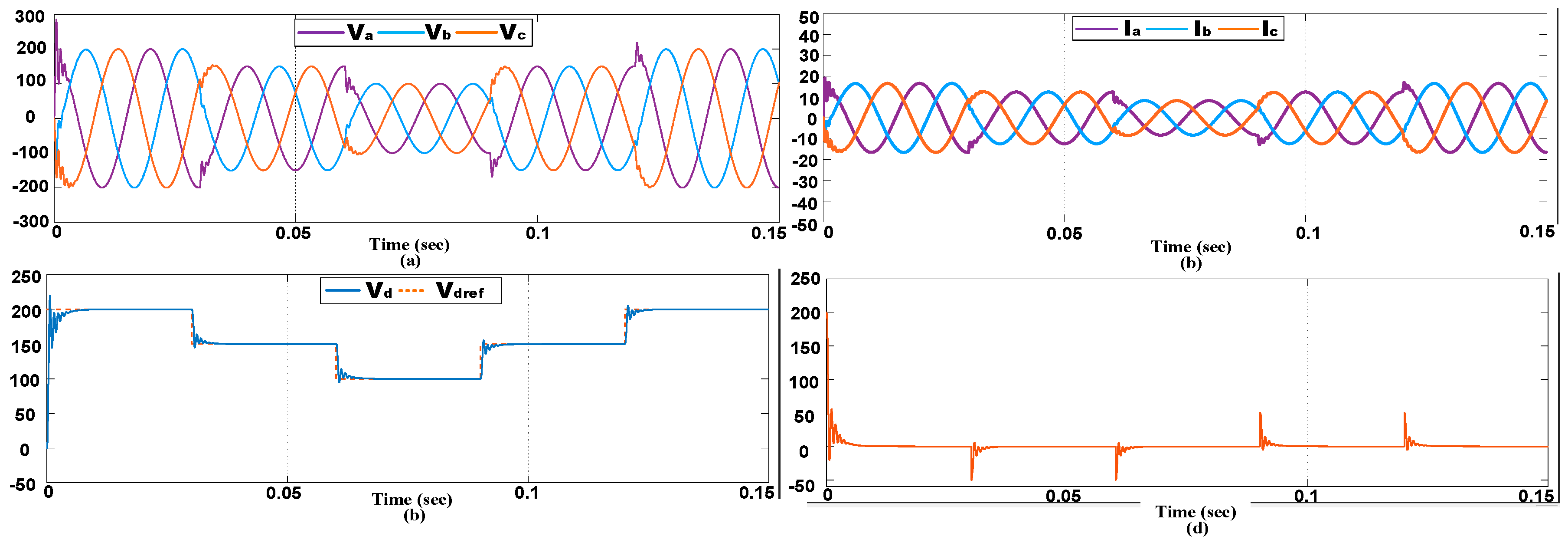
6.1.3. Transient Response with Resistive Load

The waveform of output voltage v a , v b , v c , and the load current i a , i b , i c of the H∞ robust controller, DB predictive controller, and PI controller in transient state are shown in Figure 12, Figure 13 and Figure 14, respectively. In Figure 12, Figure 13 and Figure 14, it is shown that the system is provided with a voltage change for the time instant of 300ms to evaluate its dynamic response. Here, the reference voltage level is changed from 200 V to 150 V, from 150 V to 100 V, from 100 V to 150 V, and then from 150 V back to 200 V again. The system performance was analyzed, and it was found that the transient time for the H∞ robust controller and DB predictive controller was almost negligible where the system tracked the voltage change very rapidly without any fluctuation and changed its state according to the change in the reference value. In contrast, in the case of the conventional PI controller, as illustrated in Figure 14a,b, the system had a large transient time and it required more settling time, which shows its slow dynamic performance.

7. Conclusion

This paper presents a robust control scheme proposed for a three-phase DC/AC VSI. The control scheme consists of an inner current loop and an outer voltage loop, both designed by H∞ robust control technique. The main aim is to improve the power quality of VSI having a low THD value of output voltage, both with linear and non-linear loads. This control scheme can be used for single-phase and three-phase systems. The proposed H∞ robust controller was compared with a DB predictive controller and a conventional PI controller, with a focus on improved power quality and low voltage THD. It was observed from the simulation results that the proposed controller offers a significant improvement over the DB predictive and conventional PI controllers by having better steady-state and transient responses.

Author Contributions

M.A.U.R. proposed the idea for writing the manuscript. Z.A. and M.M.K. suggested the literature and supervised in writing the manuscript. M.A.S. helped M.A.U.R. in writing and formatting. Z.A. helped in modifying the Figures and shared the summary of various credible articles to be included in this manuscript. M.M.K. helped in defining the system parameters to make the simulation test possible.

Acknowledgments

This paper was partly supported by the National Science Foundation of China (61473183, U1509211, 61627810) and the National Key R&D Program of China (SQ2017YFGH001005).

Conflicts of Interest

The authors declare no conflict of interest.

References

  1. Liserre, M.; Fuchs, F.W.; Blaabjerg, F.; Dannehl, J.; Pena-Alzola, R.; Sebastian, R. Systematic Design of the Lead-Lag Network Method for Active Damping in LCL-Filter Based Three Phase Converters. IEEE Trans. Ind. Inform. 2013, 10, 43–52. [Google Scholar] [CrossRef]
  2. Dou, C.X.; Jin, S.J.; Jiang, G.T.; Bo, Z.Q. Multi-agent based control framework for microgrids. In Proceedings of the 2009 Asia-Pacific Power and Energy Engineering Conference, Wuhan, China, 27–31 March 2009; pp. 1–4. [Google Scholar] [CrossRef]
  3. Sahoo, A.K.; Shahani, A.; Basu, K.; Mohan, N. LCL filter design for grid-connected inverters by analytical estimation of PWM ripple voltage. In Proceedings of the 2014 IEEE Applied Power Electronics Conference and Exposition- APEC 2014, Fort Worth, TX, USA, 16–20 March 2014; pp. 1281–1286. [Google Scholar] [CrossRef]
  4. Holmes, D.G.; Lipo, T.A.; McGrath, B.P.; Kong, W.Y. Optimized Design of Stationary Frame Three Phase AC Current Regulators. IEEE Trans. Power Electron. 2009, 24, 2417–2426. [Google Scholar] [CrossRef]
  5. Sangwongwanich, A.; Abdelhakim, A.; Yang, Y.; Zhou, K. Control of Single-Phase and Three-Phase DC/AC Converters; Elsevier Inc.: Amsterdam, The Netherlands, 2018; ISBN 9780128052457. [Google Scholar]
  6. Hornik, T.; Zhong, Q.C. A current-control strategy for voltage-source inverters in microgrids based on H∞and Repetitive Control. IEEE Trans. Power Electron. 2011, 26, 943–952. [Google Scholar] [CrossRef]
  7. Lee, T.; Chang, J. H∞ Loop-Shaping Controller Designs for the Single-Phase Inverters. IEEE Trans. Power Electron. 2001, 16, 473–481. [Google Scholar]
  8. Chowdhury, M.A.; Kashem, S.B.A. H∞ loop-shaping controller design for a grid- connected single-phase photovoltaic system. Int. J. Sustain. Eng. 2018, 11, 196–204. [Google Scholar] [CrossRef]
  9. Komurcugil, H. Rotating-sliding-line-based sliding-mode control for single-phase UPS inverters. IEEE Trans. Ind. Electron. 2012, 59, 3719–3726. [Google Scholar] [CrossRef]
  10. Tahir, S.; Wang, J.; Baloch, M.; Kaloi, G. Digital Control Techniques Based on Voltage Source Inverters in Renewable Energy Applications: A Review. Electronics 2018, 7, 18. [Google Scholar] [CrossRef]
  11. Quan, X.; Huang, A.Q.; Dou, X.; Wu, Z.; Hu, M. A novel adaptive control for three-phase inverter. In Proceedings of the 2018 IEEE Applied Power Electronics Conference and Exposition (APEC), San Antonio, TX, USA, 4–8 March 2018; pp. 1014–1018. [Google Scholar] [CrossRef]
  12. Espi, J.M.; Castello, J.; Garcia-Gil, R.; Garcera, G.; Figueres, E. An Adaptive Robust Predictive Current Control for Three-Phase Grid-Connected Inverters. IEEE Trans. Ind. Electron. 2011, 58, 3537–3546. [Google Scholar] [CrossRef] [Green Version]
  13. Colak, I.; Kabalci, E.; Bayindir, R. Review of multilevel voltage source inverter topologies and control schemes. Energy Convers. Manag. 2011, 52, 1114–1128. [Google Scholar] [CrossRef]
  14. Trivedi, A.; Singh, M. Repetitive Controller for VSIs in Droop-Based AC-Microgrid. IEEE Trans. Power Electron. 2017, 32, 6595–6604. [Google Scholar] [CrossRef]
  15. Mohamed, I.S.; Zaid, S.A.; Abu-Elyazeed, M.F.; Elsayed, H.M. Classical methods and model predictive control of three-phase inverter with output LC filter for UPS applications. In Proceedings of the 2013 International Conference on Control, Decision and Information Technologies (CoDIT), Hammamet, Tunisia, 6–8 May 2013; pp. 483–488. [Google Scholar] [CrossRef]
  16. Cortés, P.; Ortiz, G.; Yuz, J.I.; Rodríguez, J.; Vazquez, S.; Franquelo, L.G. Model predictive control of an inverter with output LC filter for UPS applications. IEEE Trans. Ind. Electron. 2009, 56, 1875–1883. [Google Scholar] [CrossRef]
  17. Mattavelli, P. An improved deadbeat control for UPS using disturbance observers. IEEE Trans. Ind. Electron. 2005, 52, 206–212. [Google Scholar] [CrossRef]
  18. Ibrahim Mohamed, Y.A.R.; El-Saadany, E.F. An improved deadbeat current control scheme with a novel adaptive self-tuning load model for a three-phase PWM voltage-source inverter. IEEE Trans. Ind. Electron. 2007, 54, 747–759. [Google Scholar] [CrossRef]
  19. Hornik, T.; Zhong, Q.-C. H∞ repetitive voltage control of grid-connected inverters with a frequency adaptive mechanism. IET Power Electron. 2010, 3, 925. [Google Scholar] [CrossRef]
  20. Laub, A.J.; Heath, M.T.; Paige, C.C.; Ward, R.C. Computation of System Balancing Transformations and Other Applications of Simultaneous Diagonalization Algorithms. IEEE Trans. Automat. Contr. 1987, 32, 115–122. [Google Scholar] [CrossRef]
  21. Rasool, M.A.U.; Khan, M.M.; Faiz, M.T.; Zhang, W.; Tahir, S. An Optimized Disturbance Observer Based Digital Deadbeat Control Technique for Three-Phase Voltage Source Inverter. In Proceedings of the 2018 International Conference on Electronics and Electrical Engineering Technology, Tianjin, China, 19–21 September 2018; pp. 27–33. [Google Scholar] [CrossRef]
  22. Pichan, M.; Rastegar, H.; Monfared, M. Deadbeat Control of the Stand-Alone Four-Leg Inverter Considering the Effect of the Neutral Line Inductor. IEEE Trans. Ind. Electron. 2017, 64, 2592–2601. [Google Scholar] [CrossRef]
  23. Chung, I.Y.; Liu, W.; Cartes, D.A.; Collins, E.G.; Moon, S. Il Control methods of inverter-interfaced distributed generators in a microgrid system. IEEE Trans. Ind. Appl. 2010, 46, 1078–1088. [Google Scholar] [CrossRef]
Figure 1. Schematic of the system with the H∞ robust controller.
Inventions 04 00018 g001
Figure 2. (a) Standard feedback robust control system, (b) Block diagram of the H∞ robust voltage control scheme.
Inventions 04 00018 g002
Figure 3. Sketch of a single-phase inverter.
Inventions 04 00018 g003
Figure 4. Formulation of the H∞ control problem.
Inventions 04 00018 g004
Figure 5. (a) Bode plot of the H∞ voltage controller, (b) H∞ current controller.
Inventions 04 00018 g005
Figure 6. Simulation results with the H∞ robust controller in steady-state condition. (a) Output voltage, (b) Load current, (c) α-frame voltage waveform, (d) Voltage tracking Error, (e) Voltage THD, (f) Current THD.
Inventions 04 00018 g006
Figure 7. Simulation results with the DB predictive controller in steady-state condition. (a) Output voltage (b) Load current, (c) α-frame voltage waveform, (d) Voltage tracking error, (e) Voltage THD, (f) Current THD.
Inventions 04 00018 g007
Figure 8. Simulation results with the PI controller in steady-state condition with linear loads. (a) Output voltage, (b) Load current, (c) d-frame voltage waveform, (d) d-frame voltage tracking error, (e) Voltage THD, (f) Current THD.
Inventions 04 00018 g008
Figure 9. Simulation results with the H∞ robust controller in steady-state condition with non-linear loads. (a) Output voltage, (b) Load current, (c) THD value of voltage, (d) THD value of current.
Inventions 04 00018 g009
Figure 10. Simulation results with the DB predictive controller in steady-state condition. (a) Output voltage, (b) Load current, (c) THD value of voltage, (d) THD values of current.
Inventions 04 00018 g010
Figure 11. Simulation results with the PI controller in steady-state condition. (a) Output voltage, (b) Load current, (c) THD value of voltage, (d) THD value of current.
Inventions 04 00018 g011
Figure 12. Simulation results with the H∞ robust controller in transient condition. (a) Output voltage, (b) Load current, (c) α-frame voltage waveform, (d) Voltage tracking error.
Inventions 04 00018 g012
Figure 13. Simulation results with the DB predictive controller in transient condition. (a) Output voltage, (b) Load current, (c) α-frame voltage waveform, (d) Voltage tracking error.
Inventions 04 00018 g013
Figure 14. Simulation results with the PI controller in transient condition. (a) Output voltage, (b) Load current, (c) d-frame voltage waveform, (d) Voltage tracking error.
Inventions 04 00018 g014
Table 1. System parameters.
DescriptionVariableValue
DC-Link VoltageVDC440 V
Rated Power OutputPo9 kW
Filter CapacitanceCf15 μF
Filter InductanceLf2.7 mH
Filter ResistanceRf0.1 Ω
Damping ResistanceRd1 Ω
Frequency PWMfS12.8 kHz
Table 2. Optimal gains for a proportional-integral (PI) and a dead-beat (DB) predictive controller.
ControllerGainValue
Current Loop Proportional Gainkpc3.0
Current Loop Integral Gainkic5.21
Voltage Loop Proportional Gainkpv0.1756
Voltage Loop Integral Gainkpi0.25449
Luenburger GainLM [ 5.3519 1.0460 ] T
Observer Gainη0.1
Table 3. Voltage and current THD values at steady-state condition with linear resistive loads.
ControllerH∞ RobustDB Predictive Proportional Integral
Linear Loads (Voltage)0.30%0.60%0.40%
Linear Loads (Current)1.60%3.38%2.83%
Table 4. Voltage and current THD values at steady-state condition with non-linear loads.
ControllerH∞ RobustDB PredictiveProportional Integral
Non-Linear Loads (Voltage)3.06%4.54%4.70%
Non-Linear Loads (Current)85.96%93.34%98.98%

