Abstract
In order to improve the power factor and reduce the input current harmonics, power factor correction (PFC) converters are utilized. This paper introduces a single-stage continuous conduction mode (CCM) soft-switched power factor correction (PFC) converter with a tandem topology. The proposed topology has two operating modes, namely resonant operation mode and boost operation mode. Such a design and control realizes the zero-voltage switching (ZVS) and zero current switching (ZCS) of the power switches. The proposed topology has been introduced to reduce the total harmonic distortion (THD) of the input current further in the boost PFC converter under lower power and higher output voltage conditions. The simulation and experimental results are presented to verify the effectiveness of the performance of the proposed design and its control.
1. Introduction
Power converters represent a fast-growing technology for various applications such as switch mode power supply and power factor correction (PFC) converters. To meet the harmonics standards and regulations, the PFC feature in a power supply is mandatory for various electrical and electronics applications [1,2].
Basically, PFC means lowering the reactive power and mitigating the harmonics loss to zero. Active PFC is the use of power electronics to change the waveform of current drawn by a load to improve the power factor. In the case of a switched-mode power supply, a DC-DC converter is inserted between the bridge rectifier and the main input capacitors. The DC-DC converter attempts to maintain a constant DC bus voltage on its output while drawing a current that is always in phase with and at the same frequency as the line voltage [3]. To increase the performance of PFC converters, designers have made great efforts to develop several topologies. These developments have seen the emergence of powerful and cost-effective solutions, which can achieve higher efficiency, as well as reduce the number of components [4]. Meanwhile, increasing the converter efficiency is the major driving force for the researcher to pay attention to any potential opportunities to mitigate the losses of the individual components to be used in a converter. Furthermore, optimization of and improving the efficiency of the converter in various aspects are necessary, such as devices connected in parallel, as well as the size of the boost inductor. The component that takes most of the volume in PFC converters is mainly the boost inductor [5,6].
In order to reduce the size and cost of the inductor, the waveform shape of the source current must approach a sinusoidal wave as the switching frequency increases, which reduces the total harmonics distortion (THD) [7]. However, this results in reverse recovery of the boost diode, which causes turning off loss and the boost switch turning on loss, thus increasing the size of the heat-sink [8,9]. When increasing the switching frequency to improve the quality of PFC, the above-mentioned problem will be increased. Researchers have investigated these challenges by introducing a soft-switching technique instead of a hard-switching technique, which leads to reducing the switching losses, the size and cost of the heat-sink, mitigating switching stress, eliminating electromagnetic interference and enhancing the efficiency of the converter [10]. The soft-switching technique produces resonance between passive elements, which are an inductor and a capacitor. During a switching period (turn on/off), it accordingly obtains zero current and/or zero voltage switching. Several advantages of this technique are reported in the literature, but its main shortcoming is the necessity for an auxiliary circuit to generate the resonance phenomena at switching time. The work in [11,12] introduced an auxiliary resonant circuit to operate a converter switch under the soft-switching technique. However, the conduction loss increased due to the higher RMS current. In order to reduce the switching losses, Bang, et al. [1] suggested a complicated tandem resonant circuit with sixteen operating states, which increases the circuit complexity. The main emphasis in this design is to minimize the losses rather than the THD of the input current [13].
Recently, continuous conduction mode (CCM) boost PFC converters have become an advantageous topology for designing PFC over the range of medium- to high-power applications [14]. Furthermore, the boost PFC converters are used widely due the ease of design and their simple control [15]. According to the inductor current, the boost PFC converter is categorized into two major modes: continuous current mode and discontinuous current mode [16,17].
In CCM, the ripples of the inductor current are very low. This leads to mitigation of the RMS current on the switch and lowers the electromagnetic interference issue. However, the diode suffers a reverse recovery, and the main switching is conducted under the hard-switching condition. Hence, such a converter is more suitable for medium- to high-power applications.
However, in various applications, the PFC converter for low power load is required. For these applications, discontinuous current mode (DCM) operation occurs in a zone where power that reaches the line voltage is continuously decreasing. When the output voltage is higher, the input current is more likely to go to DCM when the line voltage is close to zero with a higher ripple in the current [18,19]. When the boost PFC converter operates in discontinuous current mode (DCM), the converter switch turns on under zero current switching (ZCS), and there are no reverse recovery losses in the diode. Due to the fixed switching frequency, the design of the inductor and EMI filter is easy. Moreover, a simple and cost-effective voltage control is required. The switches and diodes, as well as inductor current RMS and peak values are higher, due to the power delivery not being utilized for the entire switching cycle. Correspondingly, current stress, switching and conduction losses of the switch are increased. Thus, this leads to the reduction of the converter efficiency and poor power factor correction, especially at the higher voltage. However, the current harmonics profile meets the standards [20].
In this paper, a novel design based on the improvement of a simple topological structure rather than the control algorithm has been proposed. The main attraction of the proposed topology is that a nearly lossless switch turned off and turned on is achieved with the soft-switching technique instead of hard-switching. The reverse recovery loss of the boost diode is minimized compared to that found in other traditional boost PFC topologies. The aim of this paper is to enhance the efficiency and the performance of the continuous conduction mode discontinuous current PFC converter. The proposed topology is similar in concept to that presented in [1]; the auxiliary circuit makes it more simplified and reduces the number of operation states. At a high instantaneous line voltage, the resonant part reduces the duty cycle, so the overall conduction losses are reduced. The auxiliary resonant circuit mainly operates at low voltage with high frequency, and this leads to minimizing the size of the converter. Therefore, the proposed structure presents the advantages of high power density and better performance. The proposed topology is especially attractive for high DC-link output voltage applications.
This paper is organized as follows. In Section 2, the topology of the proposed PFC converter is described in detail, and the operation states of the converter are introduced. In Section 3, an example is presented to show the guidelines for designing the parameters of the converter. In Section 4, the simulation results are given to show the performance of the design. In Section 5, the experiment results are presented to show the performance of the tandem PFC converter. Finally, Section 6 concludes the paper.
2. Tandem Power Factor Correction (PFC) Converter
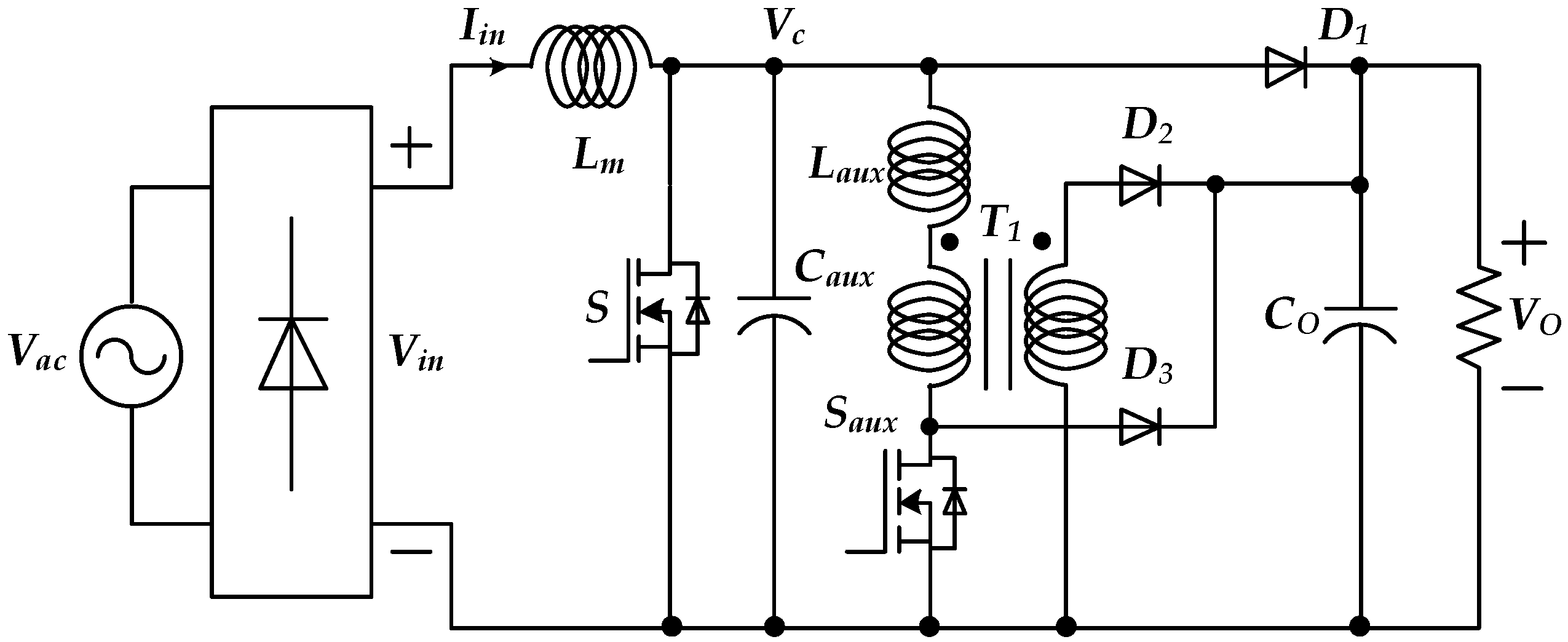
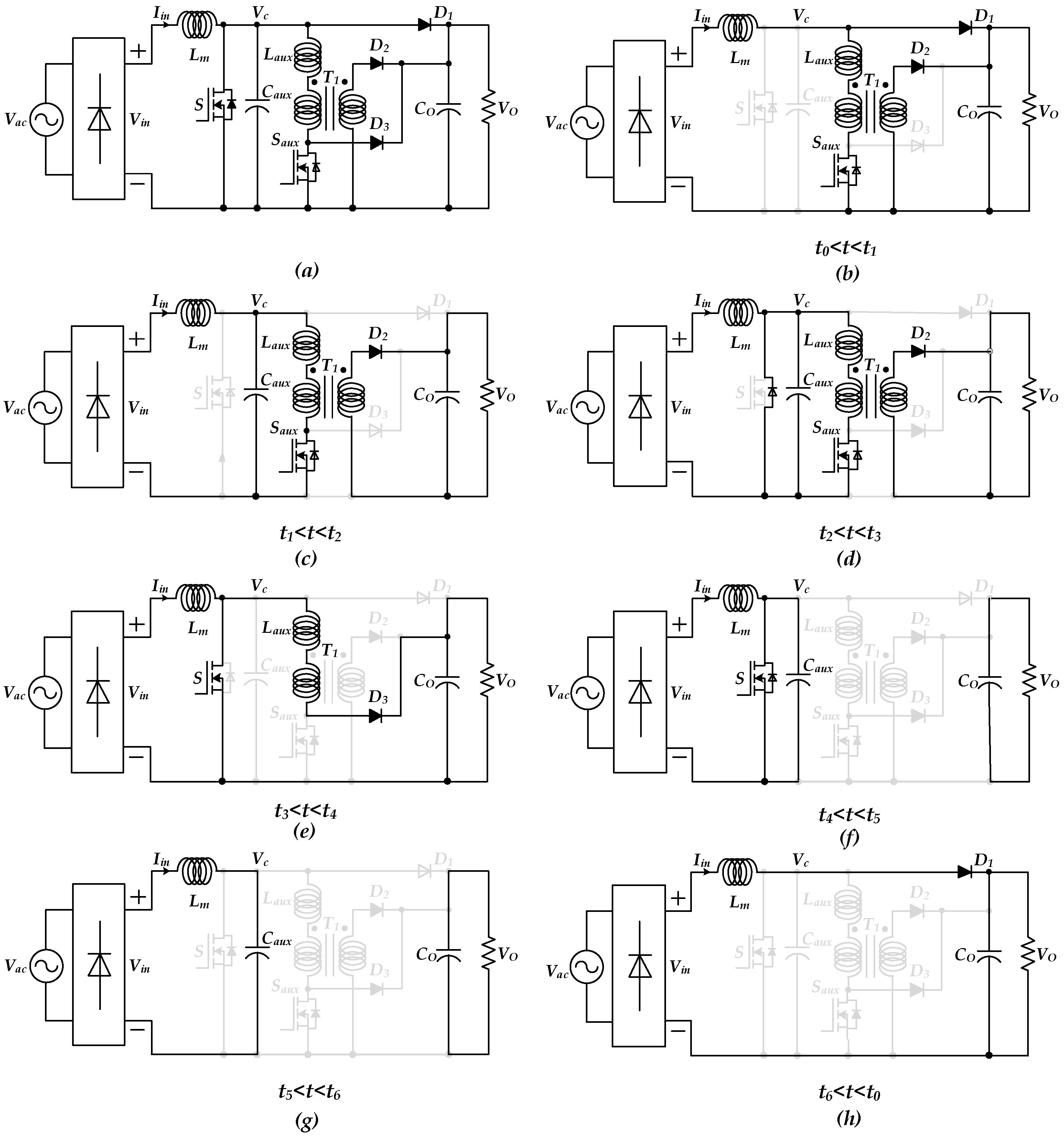
The topology of the suggested 3-kW boost PFC converter based on soft-switching PWM is presented in Figure 1. The schematic circuit diagram of the proposed tandem boost PFC converter consists of two sub-converters, that is resonant- and boost-converter. The auxiliary circuit creates the soft-switching condition for the main switch and boost diode. Further, it also minimizes the circulating energy caused by the resonant behaviors. The proposed PFC converter is a modified form of the traditional PWM boost converter of a resonant branch, which is composed of an auxiliary capacitor , auxiliary switch and a transformer . The blocking diode is utilized for transmitting unidirectional power, and is used to discharge the residual power in resonant inductor , while protects from breaking down when it turns off. The boost inductor , boost rectifier diode , main switch S and energy storage capacitor form the boost converter. Generally, auxiliary switch has a low power rating compared to main switch S, and the two-bidirectional switch of the converter consists of switches and S with antiparallel diodes.

Figure 1.
Proposed tandem boost PFC converter.
Moreover, the PWM method is implemented with the constant switching frequency, regardless of the output power and input voltage. Therefore, it guarantees the soft-switching condition in the whole operating range. It is noticed that the boost converter operates more frequently with the input voltage range from 80% to 120% of 220 V. Hence, the presented random boost-PFC converter is acceptable for this particular application. The working operation of the tandem boost converter is explained in the next sub-section.
Principle of Operation
Tandem PFC converter operation is analyzed in this section. To facilitate the explanation of the suggested converter, it can be treated as two independent modes according to the line voltage, that is: (1) resonant converter mode and (2) boost converter mode. The converter is analyzed assuming that the output voltage is constant over one switching cycle, the capacitor () has a low capacitance to operate in the discontinuous mode and the tandem converter performs as a resonant converter.
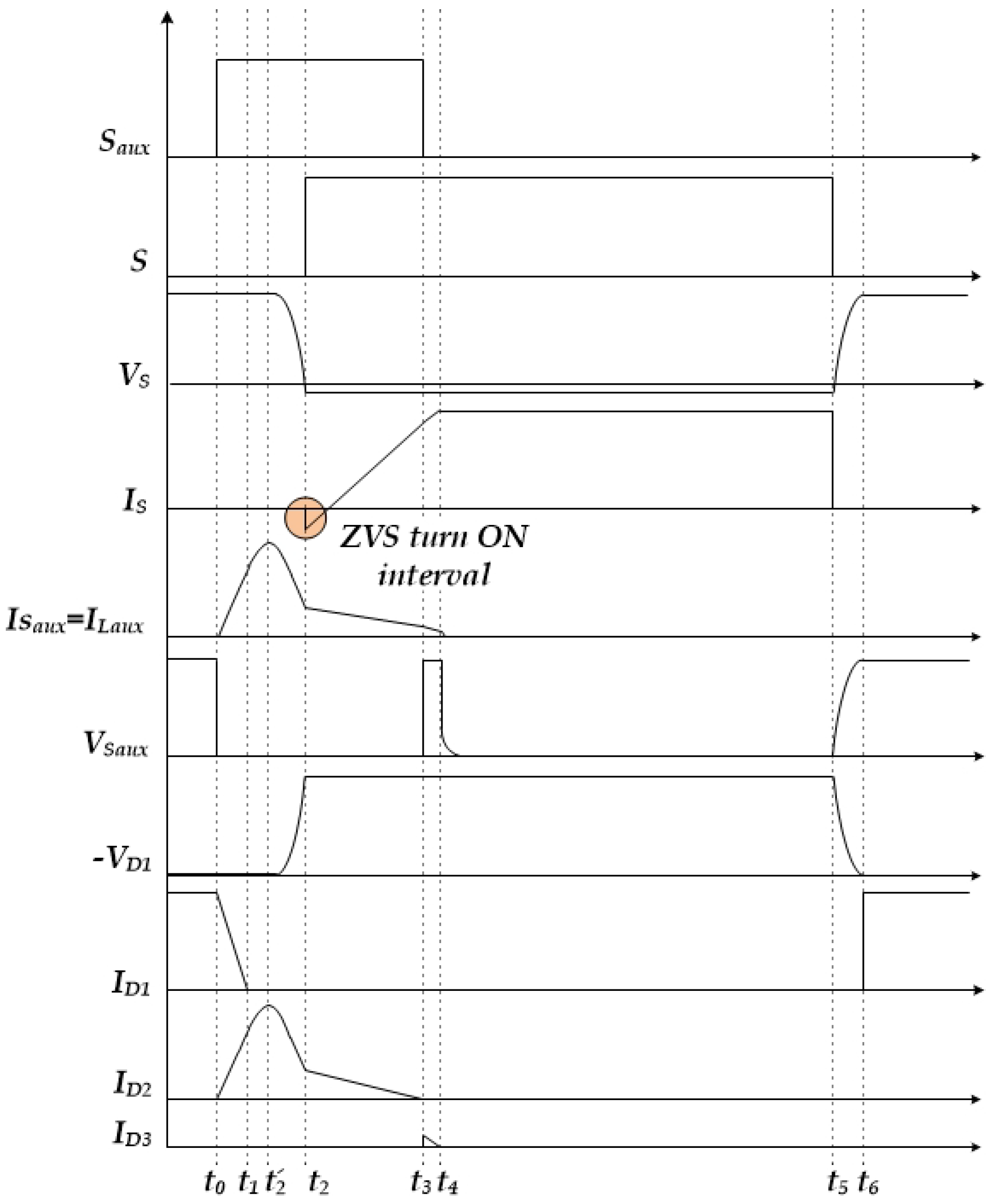
To further facilitate the analysis of the operation, Figure 2 shows the suggested converter topological modes of the converter in Figure 1, which can be divided into seven modes during a switching cycle. The waveform of the equivalent topological circuits for each stage is presented in Figure 3.

Figure 2.
Equivalent topological circuits of the proposed tandem converter. (a) Main topology diagram, (b) Stage 1: , (c) Stage 2: , (d) Stage 3: , (e) Stage 4: , (f) Stage 5: , (g) Stage 6: and (h) Stage 7: .

Figure 3.
Equivalent topological circuit theoretical waveform of the proposed tandem converter.
Stage 1 (Figure 2b, ): Before , both auxiliary switch and main switch S are turned off, and flows through the diode , while inductor is discharged into boost capacitor current . The current in both windings of auxiliary transformer is zero. During this period of time, the output voltage is equal to main switch .
At , the softly turns on at zero current, the auxiliary inductor current gradually starts to increases linearly from zero to becomes equal to at and boost diode current decrease to zero.
The time interval () of this stage can be expressed as:
Stage 2 (Figure 2c, ): This stage is divided into two time intervals and . After time interval , the resonant inductor current becomes equal to boost inductor current , then the converter initiates resonating between and . As long as where N is the transformer turn ratio, auxiliary inductor current continues to increase up to auxiliary switch peak current . The auxiliary capacitor continue to discharge through auxiliary inductor until . During this stage, the equations for the auxiliary capacitor and inductor are equal to:
The auxiliary switch peak current is obtained through the following equation:
(Figure 2d, ): In this stage, the voltage still continues to decrease as . If the auxiliary transformer voltage , then continues to decrease to zero. The boost inductor voltage and auxiliary capacitor voltage are given by:
Solving these equations for the initial and final condition and :
Here, is the impedance of the auxiliary inductor and capacitor.
Stage 3 (Figure 2d, ): The former stage ends at , when the antiparallel diode of main switch S starts conducting. The drain to the source voltage of the main switch is zero at , and it is turned on under the ZVS condition because the auxiliary capacitor voltage is zero due to the resonance condition. It is obvious from Equation (8) that will reach zero if . This resonant time period is mathematically calculated by:
The still decreases under the influence of transformer voltages. At the same time, the secondary side diode current also continues decreasing until the diode current approaches zero. The equation for auxiliary inductor current is:
Solving Equation (10) gives:
Stage 4 (Figure 2e, ): At , the current in the auxiliary inductor reduces to its minimum value. At this point, the axillary switch is turned off under hard-switching with a very small amount of residual current, and the primary side diode conducts. For an ideal transformer, this residual current would be equal to zero; however, for a real transformer, this will acquire a non-zero value and be equal to magnetization inductance current . In practice, the transformer is designed with a very large value of magnetization inductance, at least -times the leakage inductance ; consequently, the built-up leakage inductor would be very small. Here, a separate analysis for this built-up current is given for the sake of completeness. Considering the model of the transformer, it can be noticed that voltage has been applied to the magnetization inductance as long as diode is conducting. This is true till . Considering this fact, the equation for can be written as:
is constant for this interval, and can be given as:
here, is the magnetization inductance of the auxiliary transformer (). For the application developed in this paper, H and V, at s. It can be seen that will be less than 1A, considering .
Stage 5 (Figure 2f, ): This stage operates identically to the conventional PWM boost converter behavior. The current flows to the main switch S and inductor , and the auxiliary circuit is inactive.
Stage 6 (Figure 2g, ): At , the main switch S turns off under ZVS conditions, the boost diode is turned on naturally, resonant capacitor starts to charge up and the voltage across resonant capacitor becomes equal to at time period . At , the boost diode stats conducting.
Stage 7 (Figure 2h, ): At , the conventional boost converter condition is freewheeling and turns on again at . After , the operation stages restart from the initial one.
3. Converter Design Methodology
The design parameters are specified to determine the boost inductor , boost capacitor , auxiliary devices and optimal resonant frequency, and the specification is presented in Table 1. The nominal applied voltage is equal to 220 V, which has 10% tolerance. The model of the proposed boost PFC converter has been built to validate the theoretical results using the values of the design parameters.

Table 1.
Proposed converter components’ parameters.
3.1. Selection of Boost Inductor and Capacitor
The boost inductor and capacitor are the major parts of the PFC converter. The value of the boost inductor has to be as large as possible so that it can operate the converter in the continuous current mode to obtain lower current stress and minimize the current ripple. To lower the cost and size of the converter, the optimized boost inductor was design in [20] as follows:
Next, the boost capacitor is chosen based on controlling the output voltage with ripple . The ripple is selected based on the difference between the input and output powers. The boost capacitor is selected using the given mathematical equation [20]:
Here, .
3.2. Auxiliary Transformer
The turn ratio of the transformer is designed considering that the time of the voltage of the switch becomes zero while for the worst case scenario. Using Equation (9), it can be shown that N should be selected for successful commutation.
3.3. Transformer Secondary Side Diodes
and both turned off in soft mode, and the current in is quite smaller than ; however, the peak inverse voltage across is greater than , while is bigger than .
3.4. Selection of the Auxiliary Switch
After , in Figure 3, the auxiliary inductor current is higher than boost inductor current . In other words, at , the auxiliary switch current peak is higher than the value . During , the auxiliary capacitor voltage reduces to zero. The value of can easily be found by Equation (4), for given values of auxiliary inductor and capacitor .
3.5. Selection of and
For turn on commutation, the selection of these components greatly depends on the switching methods of the auxiliary and main switch. The timing of the auxiliary switch can be driven using two different approaches: the first approach is know as the active monitoring approach, and the second approach is known as the fixed switching instant. In the first approach, the auxiliary switch is initially turned on, and a variable switching instant can be obtained by monitoring the voltage across the main switch. The main switch is turned on when voltages across it approaches zero; while later, auxiliary components are designed in a manner such that a fixed switching instant for the auxiliary and main switches is implemented for ZVS turning on. In this paper, the latter approach is adopted. In this method, the auxiliary switch is turned on first, and the minimum value of ZVS turn on interval in Figure 3 is designed to be greater than interval . To start with, a minimum value for is selected, and Equations (7)–(11) are used to calculate and N such that the maximum of is smaller than the minimum of the ZVS turn on interval. If the condition is satisfied and the maximum value for is in a suitable bound, the main switching on instant is given a fixed value equal to or greater than the maximum value of . Otherwise, a greater value for is selected, and new values for N and are designed iteratively till the design criteria are satisfied.
4. Cost and Efficiency Compression
As compared to conventional boost PFC, the cost of the proposed PFC is slightly higher. The additional cost will be added due to the auxiliary inductor, auxiliary transformer and auxiliary switch. The power rating of the auxiliary switch will be a fraction of the main switch, as current will only flow during the commutation period. The cost of the auxiliary transformer and inductor can be reduced by incorporating the auxiliary inductance in the leakage inductance of the transformer.
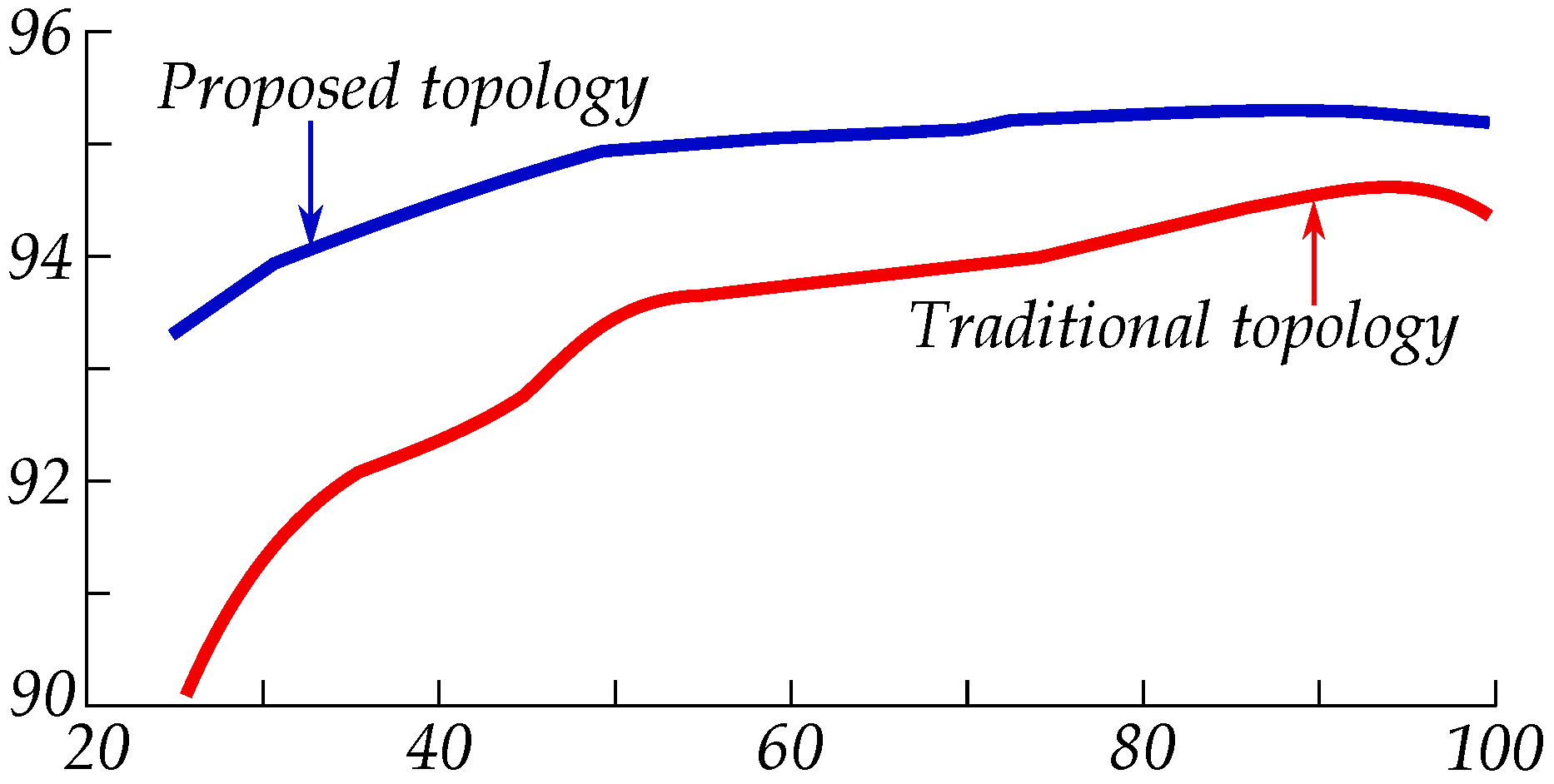
Figure 4 shows that the efficiency of the proposed converter is much higher than that of the traditional boost converter. These efficiency values for the the proposed converter and traditional converter are achieved by the power analyzer under the same conditions. The overall proposed converter efficiency is 97.4% at nominal output power. As a result, it can be clearly seen that the operation principles and predicted theoretical analysis of the proposed converter are simulated and experimentally verified.
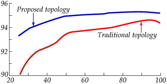
Figure 4.
Efficiency compression of the proposed and traditional PFC converters.
5. Results and Discussion
5.1. Simulation Results
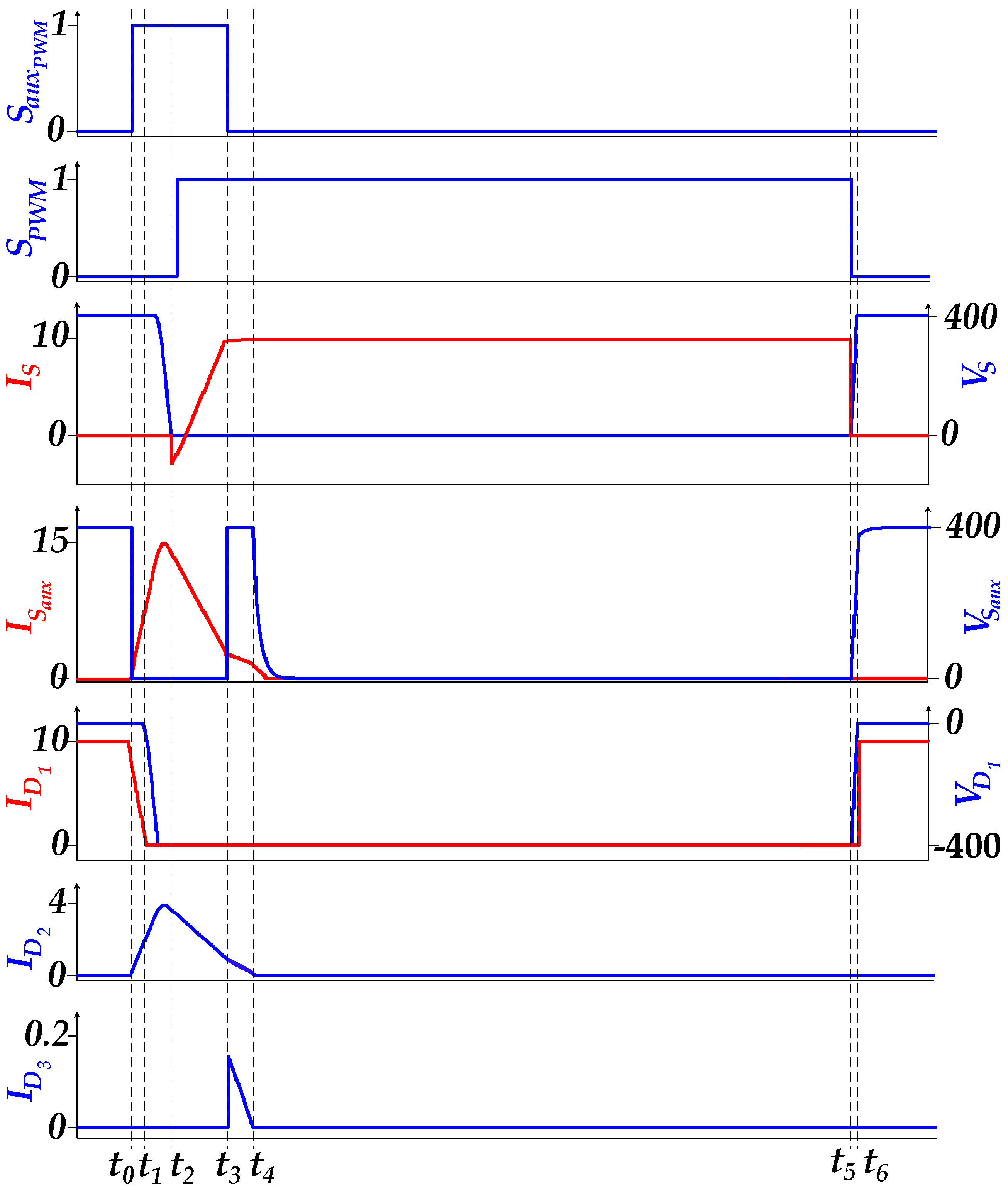
To verify the theoretical analysis of the proposed concept, the simulation model of the proposed converter was simulated in MATLAB and Simulink. The specification of simulation model is listed in Table 1. To mitigate the switching losses and achieve zero voltage switching, the auxiliary resonant circuit was composed of a fast switching device MOSFET and the passive resonant components inductor and capacitor. The simulated waveforms of the tandem converter auxiliary circuit are shown in Figure 5.

Figure 5.
Simulated waveforms of the tandem converter.
Based on the design parameters in Table 1, the designed converter was simulated and compared to a traditional boost PFC converter under three different working conditions to show the improved performance in the reduction of THD of the input current. The parameters of the boost converter were the same as those in the tandem converter, except for the auxiliary resonant circuit. The control system was based on the common average current with a fixed frequency control strategy. The delay process was used to realize the ZVS of main switch S. The simultaneous turning off of the two switches realized the ZCS of .
5.2. Comparison between the Proposed and Classical Boost Converters
5.2.1. Minimum Power and Maximum Output Voltage
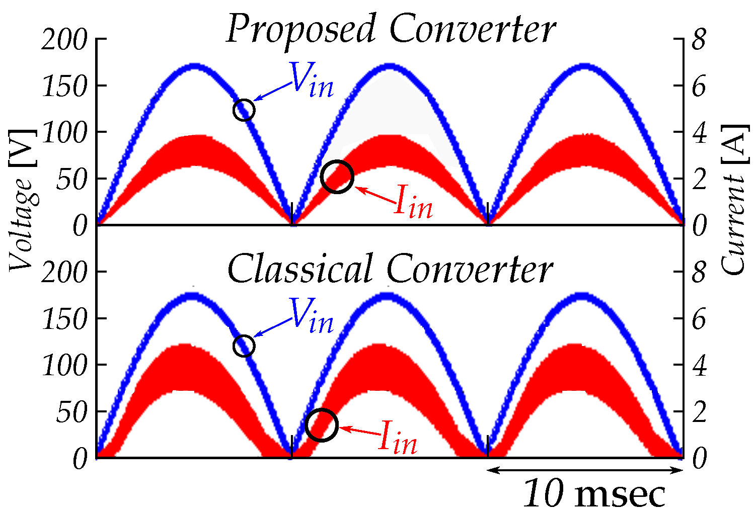
Under the severest working conditions with the minimum power and maximum output voltage, in this example from Table 1, namely V, A and V, the simulated results of the designed tandem converter and the traditional boost converter are shown in Figure 6.

Figure 6.
Comparison under the condition of minimum power and maximum output voltage.
5.2.2. Nominal Power and Nominal Output Voltage
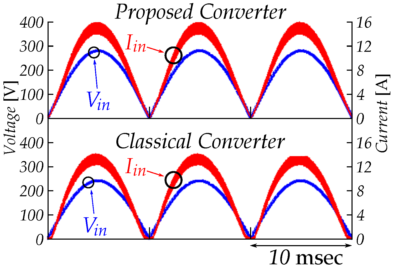
Under nominal power and nominal output voltage, from Table 1, namely V, A and V, the simulated results of the designed tandem converter and the traditional boost converter are shown in Figure 7.

Figure 7.
Comparison under the condition of nominal power and nominal output voltage.
5.2.3. Maximum Power and Minimum Output Voltage
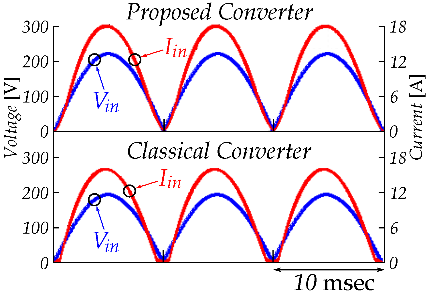
Under maximum power and minimum output voltage, from Table 1, namely V, A and V, the simulated results of the designed tandem converter and the traditional boost converter are shown in Figure 8.

Figure 8.
Comparison under the condition of maximum power and minimum output voltage.
As can be seen Figure 6, Figure 7 and Figure 8, for the boost converter, operation in DCM, which leads to large distortion of input current, occurred when the line voltage became close to zero. However, the input current of the designed tandem converter remained continuous even under minimum power and showed smaller distortion.
5.3. THD Analysis of the Input Current of the Tandem Converter
Under nominal input voltage and nominal output voltage, the THD of the input current was analyzed from minimum to maximum. The comparison between the simulation model designed tandem converter and the boost converter is given in Table 2.
Table 2.
THD analysis of the tandem and boost converters.
The most important point that should be addressed is the low THD of the input current under low input voltage and current. From the THD analysis above, it can be concluded that the THD of the input current of the tandem converter was much lower than that of the boost converter under small input current, thus improving the power quality to a large extent. As the current increased, the portion of discontinuous input current decreased, so the THD difference between the two converters decreased. Unlike the traditional boost PFC converter, when the AC input voltage was small under low load, the input current went into DCM very easily. In this design, the input current would not go to DCM because of the auxiliary resonant circuit keeping the input current continuous. Once the input current was kept continuous, the THD would be much lower. The average current control with constant frequency was applied in both working modes, thus simplifying the control system and improving the control stability.
5.4. Experimental Results
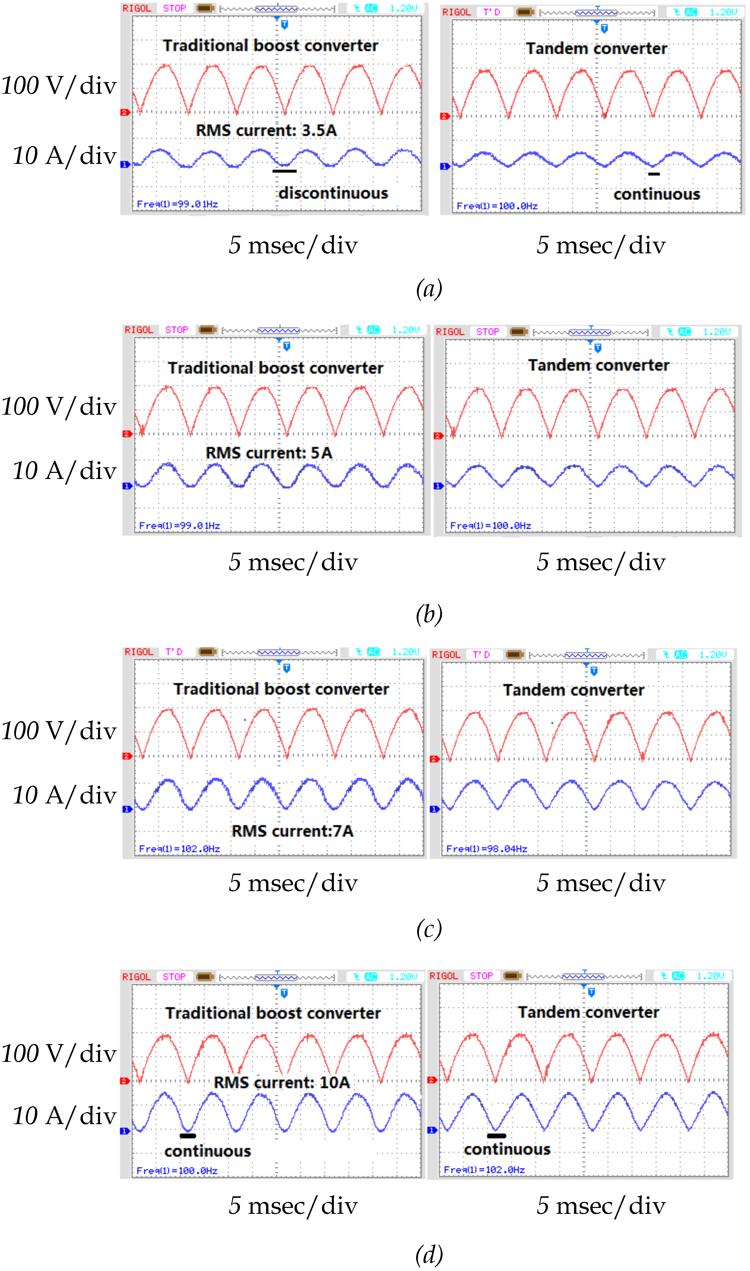
To verify the operation and performance of the proposed tandem converter, a design of a power of 3 kW has been tested in a laboratory prototype. The input RMS voltage was 140 V, while the maximum input RMS current varied from to 10 A. The specifications of the laboratory prototype were nearly the same as the design example in Section 2.
5.4.1. Comparison of the Current
When the input voltage remained the same, and the control reference input RMS current varied from to 10 A, and the input voltage and input current waveforms are shown under different conditions in Figure 9a–d. The red line in the figure represents the input voltage, while the blue line represents the input current. Under nominal input voltage and nominal output voltage, the THD of the input current was analyzed from minimum to maximum. The comparison between the experimentally-designed tandem converter and the boost converter is given in Table 3.

Figure 9.
Input current and voltage waveforms of the two converters under low input reference RMS current of (a) 3.5 A, (b) 5 A, (c) 7 A and (d) 10 A.
Table 3.
THD analysis of the tandem and boost converters.
5.4.2. Experiments of the Resonant Part
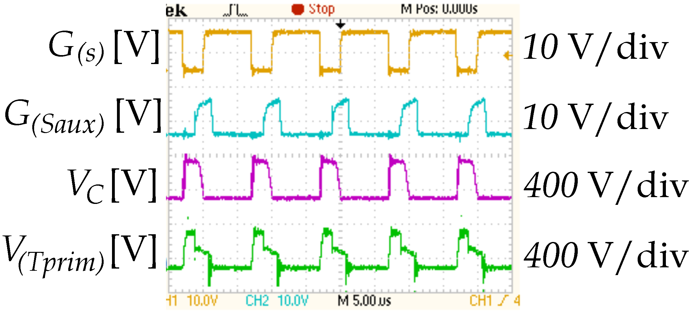
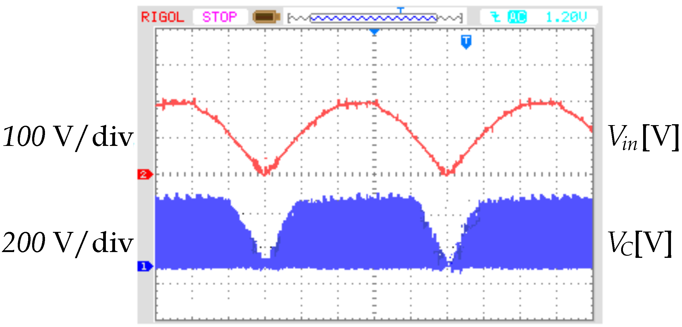
Under the stable state, the output voltage was about 400 V. The waveforms of the gate signals of switch S and and the corresponding voltage waveforms of the resonant capacitor and the primary side of the transformer during switching cycles are presented in Figure 10. The waveform of the resonant capacitor during a half line cycle is presented in Figure 11.
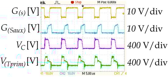
Figure 10.
Waveforms of the resonant part of the tandem converter.
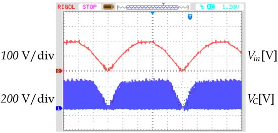
Figure 11.
Voltage waveform of the resonant capacitor during a half line cycle.
As can be seen from the experiment results, compared to the simulation results, the only difference was the turn off time of . Actually, when the resonant current became zero, the auxiliary switch could be turned off. The advantage is that this reduces the excitation loss. From the current waveforms in Figure 9, the THD of the input current was reduced compared to the traditional boost PFC converter under the light load condition. From the voltage waveform of the resonant capacitor in a half line cycle in Figure 11, the equivalent average voltage dropped down, which means the equivalent output voltage of the boost converter dropped down. Therefore, if the same duty cycle were given for the tandem converter and the traditional boost converter, obviously the tandem converter would be more capable of stepping up the output voltage. On the other hand, from Figure 10, the auxiliary resonant part took only a very small fraction of the whole volume, and the two switches realized soft-switching, thus reducing the switching loss.
6. Conclusions
A novel single-stage tandem PFC converter is proposed in this paper. The proposed tandem converter is a very attractive topology for the PFC application. Its features include fixed frequency operation, compact size and high efficiency with soft-switching for the power switches. The THD has been improved by 2% at a lower current rating, and the efficiency has improved by two percent at a higher power range. The most important function of such a converter is the reduction of the THD of the input current by keeping the input current continuous.
The analysis of the operation states of the converter and the design guidelines are given, and simulation and experiment results are presented to show the feasibility of the design.
Author Contributions
M.H. proposed the idea for writing the manuscript. X.J. and Q.B. helped in system parameters and designing to make the simulation and practical test possible and shared the summary of various credible articles to be included in this manuscript.
Funding
This paper is funded by the State Grid Changzhou Power Supply Company and Changzhou Tianman Energy Technology, Changzhou, Jiangsu, China.
Conflicts of Interest
The authors declare no conflict of interest.
References
- Bang, T.; Park, J.W. Development of a ZVT-PWM buck cascaded buck–boost PFC converter of 2 kW with the widest range of input voltage. IEEE Trans. Ind. Electron. 2018, 65, 2090–2099. [Google Scholar] [CrossRef]
- Li, Q.; Yao, K.; Song, J.; Xu, H.; Han, Y. A series diode method of suppressing parasitic oscillation for boost PFC converter operated in discontinuous conduction mode. IEEE Trans. Power Electron. 2018, 33, 407–424. [Google Scholar] [CrossRef]
- Kim, H.S.; Kim, J.K.; Park, K.B.; Seong, H.W.; Moon, G.W.; Youn, M.J. On/off control of boost PFC converters to improve light-load efficiency in paralleled power supply units for servers. IEEE Trans. Ind. Electron. 2014, 61, 1235–1242. [Google Scholar] [CrossRef]
- Badawy, M.O.; Sozer, Y.; De Abreu-Garcia, J.A. A novel control for a cascaded buck–boost PFC converter operating in discontinuous capacitor voltage mode. IEEE Trans. Ind. Electron. 2016, 63, 4198–4210. [Google Scholar] [CrossRef]
- Vahedi, H.; Shojaei, A.A.; Chandra, A.; Al-Haddad, K. Five-level reduced-switch-count boost PFC rectifier with multicarrier PWM. IEEE Trans. Ind. Appl. 2016, 52, 4201–4207. [Google Scholar] [CrossRef]
- Baek, J.I.; Kim, J.K.; Lee, J.B.; Youn, H.S.; Moon, G.W. A Boost PFC Stage Utilized as Half-Bridge Converter for High-Efficiency DC–DC Stage in Power Supply Unit. IEEE Trans. Power Electron. 2017, 32, 7449–7457. [Google Scholar] [CrossRef]
- El Aroudi, A.; Orabi, M. Stabilizing technique for AC–DC boost PFC converter based on time delay feedback. IEEE Trans. Circuits Syst. 2010, 57, 56–60. [Google Scholar] [CrossRef]
- Mallik, A.; Khaligh, A. Control of a three-phase boost PFC converter using a single DC-link voltage sensor. IEEE Trans. Power Electron. 2017, 32, 6481–6492. [Google Scholar] [CrossRef]
- Meral, M. Using active power factor correction (PFC) boost rectifiers for an improved topology of static series compensators with no energy storage. IET Power Electron. 2012, 5, 1438–1445. [Google Scholar] [CrossRef]
- Alam, M.; Eberle, W.; Gautam, D.S.; Botting, C. A soft-switching bridgeless AC–DC power factor correction converter. IEEE Trans. Power Electron. 2017, 32, 7716–7726. [Google Scholar] [CrossRef]
- Moschopoulos, G.; Jain, P.K.; Liu, Y.F.; Joos, G. A zero-voltage-switched PWM boost converter with an energy feedforward auxiliary circuit. IEEE Trans. Power Electron. 1999, 14, 653–662. [Google Scholar] [CrossRef]
- Lu, D.D.C. High voltage stress in single-phase single-stage PFC converters: Analysis and an alternative solution. IEEE Trans. Ind. Electron. 2016, 63, 133–143. [Google Scholar] [CrossRef]
- Mallik, A.; Ding, W.; Shi, C.; Khaligh, A. Input voltage sensorless duty compensation control for a three-phase boost PFC converter. IEEE Trans. Ind. Appl. 2017, 53, 1527–1537. [Google Scholar] [CrossRef]
- Bodur, H.; Yıldırmaz, S. A new ZVT snubber cell for PWM-PFC boost converter. IEEE Trans. Ind. Electron. 2017, 64, 300–309. [Google Scholar] [CrossRef]
- Musavi, F.; Edington, M.; Eberle, W.; Dunford, W.G. Control loop design for a PFC boost converter with ripple steering. IEEE Trans. Ind. Appl. 2013, 49, 118–126. [Google Scholar] [CrossRef]
- Yao, K.; Hu, W.; Li, Q.; Lyu, J. A novel control scheme of DCM boost PFC converter. IEEE Trans. Power Electron. 2015, 30, 5605–5615. [Google Scholar] [CrossRef]
- Cheng, W.; Song, J.; Li, H.; Guo, Y. Time-varying compensation for peak current-controlled PFC boost converter. IEEE Trans. Power Electron. 2015, 30, 3431–3437. [Google Scholar] [CrossRef]
- Huber, L.; Irving, B.T.; Jovanovic, M.M. Open-loop control methods for interleaved DCM/CCM boundary boost PFC converters. IEEE Trans. Power Electron. 2008, 23, 1649–1657. [Google Scholar] [CrossRef]
- Jang, Y.; Jovanovi, M.M.; Dillman, D.L. Soft-switched PFC boost rectifier with integrated ZVS two-switch forward converter. IEEE Trans. Power Electron. 2006, 21, 1600–1606. [Google Scholar] [CrossRef]
- Kim, Y.W.; Kim, J.H.; Choi, K.Y.; Suh, B.S.; Kim, R.Y. A novel soft-switched auxiliary resonant circuit of a PFC ZVT-PWM boost converter for an integrated multichip power module fabrication. IEEE Trans. Ind. Appl. 2013, 49, 2802–2809. [Google Scholar] [CrossRef]
© 2018 by the authors. Licensee MDPI, Basel, Switzerland. This article is an open access article distributed under the terms and conditions of the Creative Commons Attribution (CC BY) license (http://creativecommons.org/licenses/by/4.0/).