Article

RF Characterization and Beam Measurements with Additively Manufactured Fast Faraday Cups

1
Informationstechnik-Elektrotechnik-Mechatronik (IEM), Technische Hochschule Mittelhessen, 61169 Friedberg, Germany
2
Institute for Accelerator Science and Electromagnetic Fields (TEMF), Technische Universität Darmstadt, 64289 Darmstadt, Germany
3
GSI Helmholtzzentrum für Schwerionenforschung, 64291 Darmstadt, Germany
4
Fraunhofer Institut für Werkstoff- und Strahltechnik (IWS), 01277 Dresden, Germany
*
Author to whom correspondence should be addressed.
These authors contributed equally to this work.
Instruments 2025, 9(4), 32; https://doi.org/10.3390/instruments9040032
Submission received: 6 August 2025 / Revised: 11 November 2025 / Accepted: 14 November 2025 / Published: 28 November 2025

Abstract

The early stages of most particle accelerator chains produce sub-ns bunches with velocities in the range of 1% to 20% of the speed of light. Fast Faraday Cups (FFCs) are designed to measure the longitudinal charge distribution of these short bunches of free charges. Coaxial designs have been utilized at the GSI Helmholtz Centre for Heavy Ion Research (GSI)’s linear accelerator UNILAC to characterize ion bunches with bunch lengths ranging from a few hundred ps to a few ns. The typical design goals are to avoid the pre-field of the charges and to suppress secondary electron emission (SEE) while preserving the capability of bunch-by-bunch measurements. This contribution presents a novel FFC design manufactured using additive manufacturing, e.g., laser powder bed fusion (LPBF), and compares it with a traditionally produced FFC. The article highlights the design process, RF characterization, and selected measurements with ion beam carried out at GSI.

1. Introduction

In accelerator instrumentation, Faraday cups represent a class of diagnostic devices specifically designed to directly collect and quantitatively measure the charge deposited by incident particle beams. Faraday cups provide absolute measurements of beam current and are widely known for their robustness, simplicity, and reliability in a variety of accelerator applications.
Faraday cups modified to measure the fast temporal evolution of charges are referred to as Fast Faraday Cups (FFCs). The temporal evolution of the measured bunch charge Q b or longitudinal charge distribution is also referred to as the shape of the bunch. In literature, many different FFC designs have been proposed, such as stripline, microchannel, multi-aperture, planar, and conical geometries [1,2,3,4,5,6,7]. Regardless of the RF signal guiding mechanism or form factors, all FFCs are designed as broadband detectors to achieve the necessary temporal resolution for their specific use case. For bunches at the linear accelerator UNILAC of GSI Helmholtz Centre for Heavy Ion Research (GSI), bunch lengths σ b of a few hundred p s to a n s are observed, and accordingly, a bandwidth of 1  G Hz to 5 G Hz is aimed for. This bandwidth regime can be conveniently covered by coaxial FFC designs. The primary challenge in measuring the charge distribution of particles with beam velocities β < 1 lies in the significant alteration of both the charge distribution and its electromagnetic field distribution caused by Lorentz boost and transformation [8]. This effect becomes especially prominent for slow beams ( β < 0.25 ) with short bunches (< n s ).
A common method for mitigating the influence of the pre-field on the detector signal is to add electrostatic shielding such as fine-mesh grids [2] or small-aperture pinholes [1,7]. The second challenge for FFCs is the effective suppression of secondary electrons (SEs), which are emitted both by the direct impact of impinging ions and by the interaction with high-energy SEs generated within the detector materials. The presence of SEs can significantly alter the measured bunch shape, making robust suppression mechanisms indispensable for retrieving the true, undisturbed bunch shape. The established methods include field-based suppression and geometric mitigation: Field-based suppression involves the application of electric [2] or magnetic fields to confine the SEs within the FFC. Geometric mitigation modifies the geometry of the collector of the FFC, e.g., conically, to redirect the main direction of the emitted SEs toward surfaces where they are rapidly reabsorbed [9].
In this contribution, we aim for high-quality bunch shape measurements with FFCs only, and do not focus on absolute charge measurements, which is another key feature of Faraday cups. Because many FFC designs select only a portion of the beam, it is not possible to directly measure the absolute charge of the entire bunch for such selective designs. The necessary bandwidth for the desired temporal resolution of bunch-by-bunch shape measurements affords rather small geometries, such that cooling of the collector becomes usually unfeasible, which would be necessary for full power or absolute charge measurements. We begin with a systematic analysis of axially and radially coupled coaxial FFCs with respect to their secondary electron suppression performance as simulated in CST Studio Suite™(CST) [10]. Subsequently, an optimized coaxial tapered radially coupled Fast Faraday Cup (TRCFFC) design tailored to our use cases is presented. Detailed RF simulations are shown in comparison to the previous design. We provide insights into the manufacturing processes and construction details. This design demonstrates a significant improvement in secondary electron suppression and signal-to-noise ratio for bunch-by-bunch measurements at the cost of a reduction in bandwidth. Finally, beam measurements carried out at the GSI experimental cave X2 comparing the two radially coupled designs are presented.

1.1. Working Principle of Axially Coupled FFCs

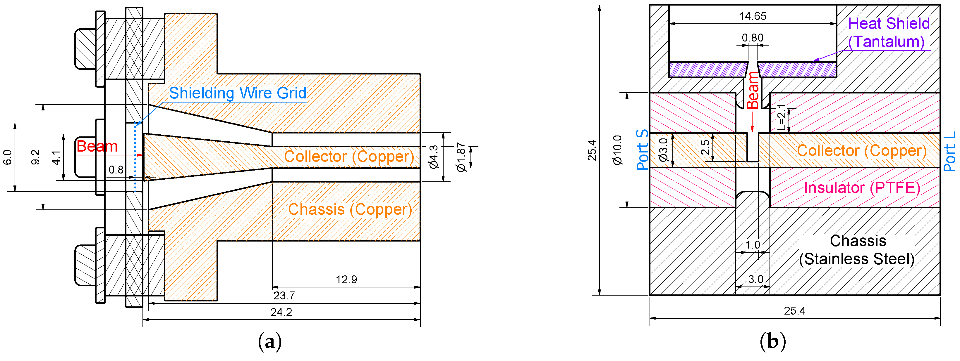
Axially coupled coaxial FFCs were first documented in literature in the 1980s [11,12], employing coaxial geometries where the beam deposits charge on the inner conductor of the tapered end of the coaxial line. A representative commercial design [2] of this type of FFC is shown in Figure 1a, optimized to ensure that the beam interaction occurs exclusively with the collector, being the inner conductor of the FFC. Usually, this is achieved with a collimator in front of the grid to limit the transversal beam width. The collimator is removed in simulations to reduce the complexity of the model, though the transversal beam width can be controlled in the simulation. The grid in front of the collector, with a distance of 0.85   m m , is used to apply an electrical field between the collector and the grid to suppress the secondaries and shield the pre-field of the bunch. A single Gaussian bunch of 34,680 Ar10+ ions is simulated with a bunch length of σ b = 100   p s and a velocity β = 0.15 . The collector is set to a static potential while the grid is kept at ground. In this configuration, the collector attracts the SEs. The effect of the SEs can be studied in the simulations by varying the potential, as shown in Figure 2. This contribution focuses only on simulation results and refers to [13] for measurement results using this type of FFC.
In the simulations, a solely ion-induced secondary electron emission (SEE) originating from the collector is allowed. The secondary electron yield and corresponding energy spectra have been extensively investigated in the literature [14,15,16,17], with recent research focusing on their application in profile grids for transverse ion beam profile measurements [18]. The approximated backscattered secondary electron yield (SEY) per ion can be derived from the Bethe–Bloch formula, which quantifies the stopping power of a charged particle beam interacting with a target. Consequently, the number of SEs N e scales with the square of the incident ion’s charge state Z, the number of incident ions N ion , and the target electron density n e of the FFC material [13]:
N e n e Z 2 · N ion .
To achieve maximum SEY, the energy dependency of the Bethe–Bloch formula is disregarded, although the kinetic energy of the ions exceeds the threshold energy E threshold to emit SEs of copper [19,20]. In this worst-case scenario, a SEY of N e = 50 SEs per ion is estimated for an Ar10+ beam. The value matches with empirical estimates reported in the literature of about 10–15 electrons per 8.0   M e V /u O 5 + ion incident to the normal incident on a copper target [16,19,20]. We use the import emission model of CST in the simulations. Note that in the following a index 0 refers to the primary particle, in our case ions. The SEY curve δ E 0 , Θ 0 is defined by the user for the primary particle energy E 0 and only for the normal incidence angle Θ 0 = 0 . We estimate the normal incident SEY to N e in the simulated energy regime of the ions. According to the documentation of CST 2024 [10], the general angular dependency on an arbitrary incident angle Θ 0 is internally calculated from the user input using the relations given in Equations (2) and (3):
E 0 ( Θ 0 ) = E 0 E threshold 2 π 2 π + Θ 0 2 + E threshold ;
δ ( E 0 ( Θ 0 ) , Θ 0 ) = δ ( E 0 ( Θ 0 ) , 0 ) 1 + Θ 0 2 2 π ,
where δ ( E ( Θ 0 ) , 0 ) is the SEY at normal incidence ( Θ 0 = 0 ) for the altered primary particle energy E 0 ( Θ 0 ) . The energy of the secondary particles follows a gamma distribution f ( E e ) :
f ( E e ) = δ E 0 ( Θ 0 ) , Θ 0 E e T e 2 e E e T e P 1 2 , E 0 T e ,
with the incomplete gamma distribution P, the most common energy T e (also denoted as temperature of the SEs), and the energy of the secondary electron E e . The Surface roughness is neglected by CST in the imported emission model [10], hence a secondary electron emission probability f ( Θ ) = c o s ( Θ ) is used, as it is characteristic for smooth surfaces [21].
Typically, the temperature of SEs is in the range of 5 e V to 10 e V [14,15]. To represent a worst-case scenario regarding the influence of the SEs, the T e was set to 10 e V in the simulations. Consequently, for an electron temperature T e of 10 e V , 96% of the SEs have energies below 50 e V . Depending on the bias voltage, this percentage represents the number of SEs that return to the collector. It should be noted that the secondaries are emitted from the conductor, propagate into free space, and, after being decelerated, subsequently regain velocity toward the collector. The process introduces a temporal delay due to the travel time of the SEs. The extent to which the bias voltage exceeds the energy of the SEs determines how quickly the point of return is reached. To show this effect, we analyze in detail the impact on the output signal of the axially coupled Fast Faraday Cup (ACFFC), which also applies to the bias-suppressed SEs of the radially coupled FFCs.
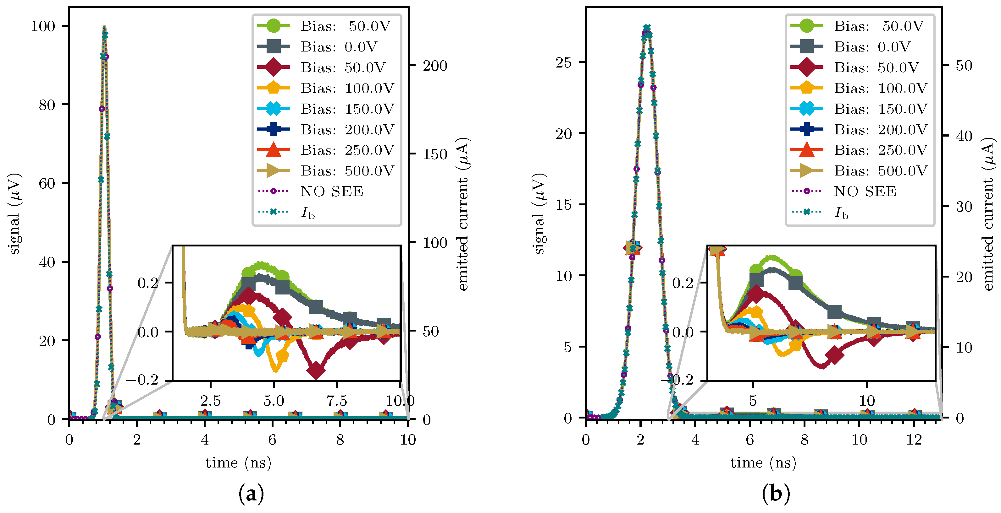
The PIC simulation results of the design depicted in Figure 1a are presented in Figure 2 with bias voltages configured between 50   V and 500 V . The ground truth of the bunch shape is given by the current I b (dashed dark blue line). If there are no SEs activated in the simulation, the current I b overlaps with the unaltered output signal “No SEE” (red dots) almost perfectly. We adjusted the current axis (right axis), such that the peak amplitude of I b and “No SEE” match to visually guide the comparison of both shapes. There is a shielding wire grid 0.8   m m in front of the collector. This grid is always kept at ground potential. It prevents the pre-field of the bunch from coupling into the collector too early and thus inducing a premature signal. The elongation of the measured shape is minimized due to this short distance to a few p s before the actual charges reach the collecting surface. If we also account for SEs, the bunch shape is strongly influenced and applying a bias scheme to suppress the SEs is necessary. A total of three different regimes can be identified within the bias schemes.
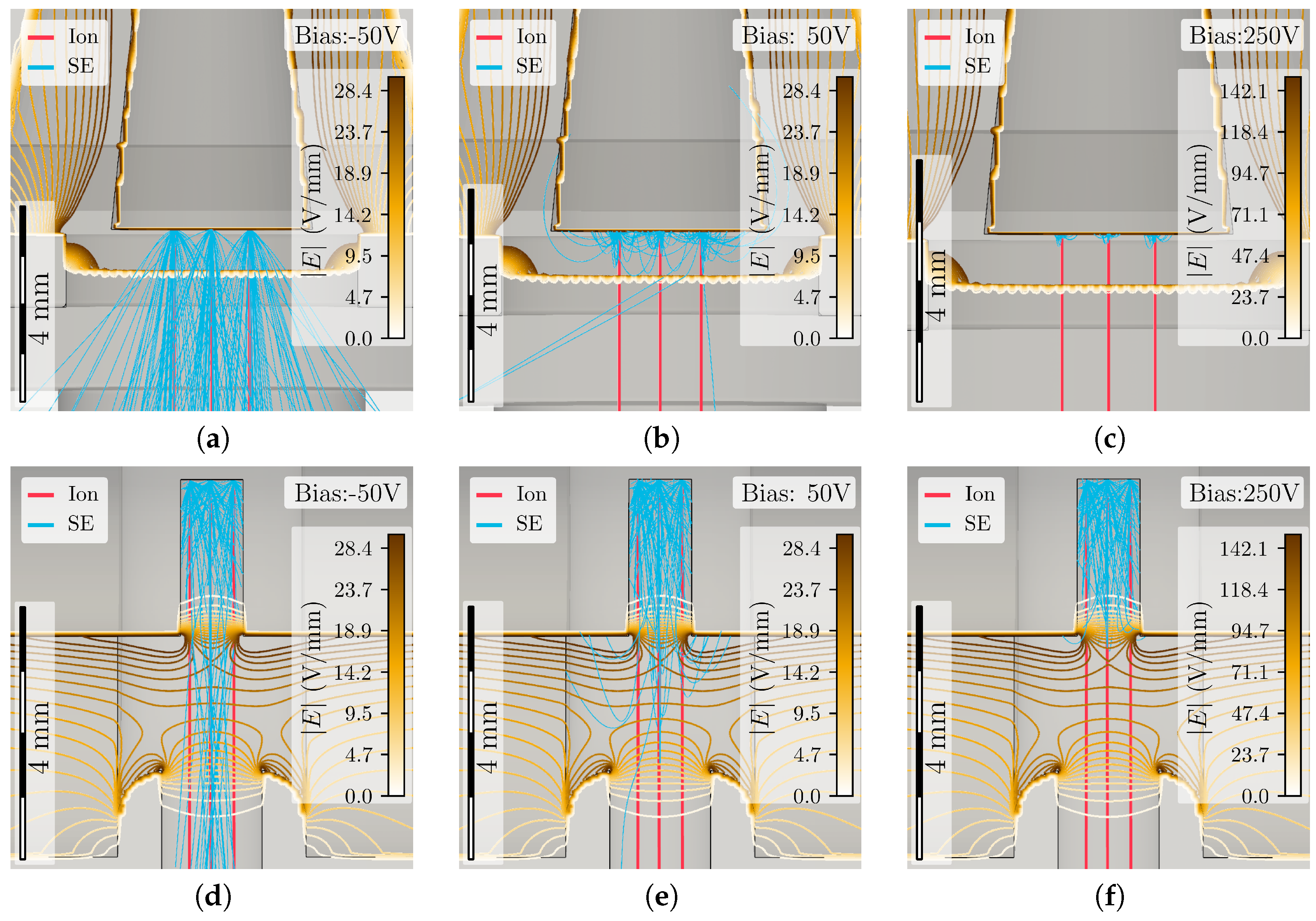
In the first regime, the collector is negatively biased. As a result, the SEs are pushed away from the collector and do not return (see Figure 3a). As the SEs move further from the collecting surface, their electric field coupled to the collector weakens, while an increasing fraction of the field strength is instead terminated on the shielding grid or chassis. The mirror charges, which become progressively less bound to the SEs, are able to move more freely and thereby generate an additional positive signal with minimum delay, ultimately increasing both signal amplitude and signal width. The influence of SEs on the signal depends on their speed, and thus on T e . While negligible at high negative bias, their energy distribution becomes evident under unbiased conditions (0 V ). The clearly visible long tail reflects the energy distribution of the SEs. The fast SEs mainly increase the total signal strength, while the slow SEs primarily extend the tail.
The second regime is characterized by the application of a moderate positive bias. In this regime, the SEs have enough energy to travel a considerable distance from the collecting surface, allowing the mirror charges in the collector to be partially transferred to the output (see Figure 3b). This initially results in an increase in the signal strength. Then, SEs with less energy than the bias voltage return, creating a negative output signal without generating a significant number of tertiary electrons due to their low energy. These returning SEs are partially compensated by the mirror charges of newly generated SEs until the production of the new SEs equals the returning SEs. Any additional SEs beyond the compensated ones contribute to a negative time-delayed signal, ultimately causing the underswing after the main peak.
The third regime refers to high biasing (>200 V , see Figure 3c). In this case, the SEs do not travel far into free space. Consequently, the mirror charges remain stationary and recombine with the SEs, resulting in no change in either signal strength or signal width. Typically, a small portion of high-energy SEs still reach far enough so that a tiny underswing remains. The ACFFC applies only a single method to suppress SEs using a bias voltage, which makes it extremely vulnerable to improper configurations. Only at high bias settings (≥250 V), the analyzed FFC can be used reliably for both bunch shape measurements and charge measurements. A too-low bias will significantly alter shape and amplitude. Additionally note that there is no interaction of the beam with the shielding grid in our simulations, which could also produce additional SEs.

1.2. Working Principle of Radial Coupled FFCs

Effective suppression of SEs based solely on a bias scheme is challenging. In general, it is advisable to combine different methods to suppress SEs, reducing the impact on the output signal as much as possible. An example of combined biasing and geometrical suppression of SEs is provided by the second design shown in Figure 1b, which features a radially coupled FFC. The collector of the RCFFC is fabricated with an outer diameter of 3 mm and contains a radially drilled hole with a diameter of 1 mm and a depth of 2.5 mm. In the simulation, the bottom of the drill hole is modeled as flat, whereas in practice, drills typically have a point angle of 115 ° to 138 ° , resulting in a short, conical end of the hole. A heat shield with a pinhole of 0.8 mm is used to limit the power entering the RCFFC protecting the collector. It also shields the pre-field of the bunch. The small diameter of the drift passage behind the pinhole shields the pre-field as well, such that the pre-field can only propagate in front of the bunch in the gap between chassis and collector. While the general distance between collector and chassis is 3 mm, a reduced diameter section extends the drift passage in the chassis, reducing the critical distance to the collector to 2.1 mm. This also helps to generate higher field strengths so that the SEs will return earlier and match the geometry to 50 Ω. In Figure 4, the bias scheme for the RCFFC for two different bunch lengths is shown.
An RCFFC has two ports instead of one for the ACFFC, splitting the signal equally. Hence, the maximum amplitude of the ion signal of the ACFFC (see Figure 2 case “NO SEE” and Bias 500 V) per port is halved. On the other hand, two ports allow for different noise suppression schemes during the signal processing. For short bunches (Figure 4a), the ions are detected without any deviation from the baseline without SEE matching the exact ion current regardless of the bias used. Only the signal part of the SEs after the ion peak is bias-dependent. The number of detected SEs is reduced by a factor of about 25 compared to the ACFFC, because the majority of the SEs hit the collector inside the drill hole, recombining with their mirror charges as seen in Figure 3 (bottom). However, a small portion of SEs escape the geometrical suppression and travel upwards along the drill hole together with their corresponding mirror charges. At the edge of the collector drill hole, the mirror charges cannot follow the SEs and will be released as soon as the electrical field of the SEs terminates on other surfaces except the collector itself. These remaining SEs can be suppressed further with a bias voltage leading to the same behavior as described for the ACFFC, but delayed by the time the SEs need to travel through the drill hole.
If the bunches become longer (Figure 4b), both the signal of the ions and the SEs overlap. However, the SE peak is significantly delayed after the ion peak. The remaining increase in the ion peak due to the SEs is still negligible in this case. The effect of the SEs can still be suppressed taking the biasing into account. For even longer bunches, the benefit of the separation is lost and only the reduction in the total number of SEs remains. The pinhole in the heat shield strongly reduces the signal amplitude compared to an ACFFC while relying primarily on the bias scheme for suppression. Therefore, the drill hole depth should be adjusted to the expected bunch length. According to the gamma-distributed SEs, the velocity v e of 96 ( < 50   e V ) of SEs is lower than 4.2   m m / n s 1 . The separation time t sep for each velocity v e can be calculated for a given expected bunch length σ b to optimize the drill hole depth of an RCFFC:
t sep = l drill v e 4 σ b .
Figure 5 shows the separation time t sep for different kinetic energies and bunch lengths. The dashed line represents the cumulative portion of SEs with a kinetic energy above E kin . If the separation time is positive, SEs with energy specified or lower are separated from the ion signal. Conversely, if the separation time is negative, all SEs with kinetic energies above this threshold overlap with the ion peak.
The RCFFC shown in Figure 1b has a drill hole depth of 2.5   m m . For a bunch length of σ b = 100   p s , no overlapping SEs are expected, which aligns with the simulation results in Figure 4a. However, for a bunch length of σ b = 400   p s , SEs with an energy above 6.9   e V (85% of all SEs) will leave the drill hole too early, causing the signal of the SEs to overlap, as shown in Figure 4b. Increasing the drill hole depth to 8 mm ensures that the signal of SEs with a kinetic energy below 71.1   e V ( 99.36 % of all SEs) remains separated, with only rare fraction ( 0.64 %) of faster SEs overlapping. Thus, adjusting the drill hole depth depending on the expected bunch lengths helps to reduce the impact of the SEs on the measured signal.

2. Additively Manufactured Tapered Radially Coupled FFC

In this section, details regarding the layout and design choices for the TRCFFC are provided, and the differences between conventionally machined and additively manufactured collectors are discussed. The comparisons are supported by simulations and measurements of the TRCFFC’s RF properties. The final design is compared to a RCFFC measuring an Ar10+ particle beam at the GSI linear accelerator UNILAC measured in the beamline X2.

2.1. Tapered Radially Coupled FFC Design Considerations and Simulations

A new variant of the previously discussed RCFFC has been developed for UNILAC at GSI. The optimization objectives are defined as achieving a higher signal-to-noise ratio and enhancing the geometric suppression of SEs for bunch lengths between 100 ps to 400 ps at velocities ranging from 5% to 15% of the speed of light. The new design is shown in Figure 6. The diameter of the pinhole in the heat shield has been increased from d RCFFC = 0.8   m m to d TRCFFC = 1.8   m m . Comparing different pinhole sizes, a theoretical signal gain of 5.1 is achievable for a uniform distribution. This gain is determined by the ratio of the pinhole areas in the two designs. The projected gain is reduced when considering the Gaussian profile of the transversal bunch shape. If the transversal profile is a strong ellipsoid, we can estimate the gain f gain by
f gain = erf 1 2 2 d TRCFFC σ b , trans erf 1 2 2 d RCFFC σ b , trans
where erf is the Gauss error function and σ b , trans the dominant transversal beam size effectively reducing it to a 1D estimation. This estimation will be met if, e.g., the beam in x-plane is significantly larger than in y-plane. Assuming a dominant transversal beam size of σ b , trans = 2   m m , the actual gain is approximately a factor of 2.19. If the beam is symmetric in both planes, the estimation of f gain should be done by comparing the integrated charge density limited by the radii of the heat shield pin holes using Equation (7). Using the same example values as for the 1D estimation, the gain for a symmetrical beam would be a factor 4.86.
f gain = 1 exp d TRCFFC 2 8 σ b , trans 1 exp d RCFFC 2 8 σ b , trans
The drift passage width of 2.2   m m inside the chassis directly after the heat shield pinhole is larger than the pinhole itself, ensuring that entering particles reach the drill hole in the collector without prematurely hitting the drift passage walls. Consequently, the collector drill hole also needs to have a larger diameter ( 2.3   m m ) than the drift passage width to prevent generation of secondaries at the surface of the collector aside inside the drill hole.
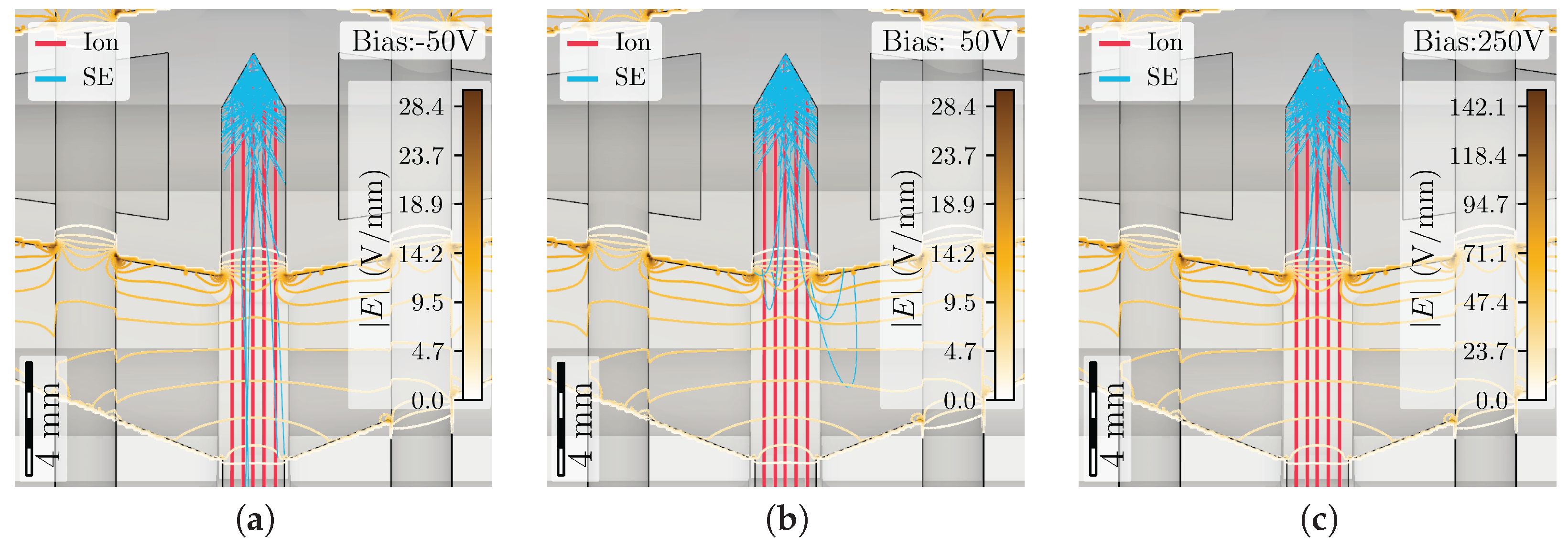
The number of SEs leaving can be controlled by the depth-to-aperture ratio of the drill hole [7]. This ratio is 2.5 for the RCFFC design. A minimum drill hole depth of 5.75   m m is needed to reach at least the same depth-to-aperture ratio for a drill hole diameter of 2.3   m m . However, at these values, 11.75 % of the leaving SEs will not be separated from the ion-induced signal for σ b = 400   p s . Thus, a drill hole depth of 8 mm was chosen, with the last 2 mm featuring a 60 ° cone-shaped end. This cone-shaped termination of the drill hole facilitates the redirection of SEE toward the hole walls, as described by Equations (3) and (4). A study of various Faraday cup geometries has been performed in [9], enabling the assessment of the effect of different drill hole terminations such as flat or wide and narrow cone-shaped on SE suppression. While a flat-ended drill hole results in a main direction of the SEs backward out of the hole, the cone-shaped tips considerably increases SE absorption at the hole walls as can be seen by comparing the results of Figure 3 (bottom) with Figure 7. Despite of the five instead of three ions, the number of SEs escaping the geometrical suppression is even lower for the TRCFFC than the RCFFC, while the quality of the bias field remains similar.
A more detailed analysis with respect to the angle of the cone shape has been performed in [7]. It was found that a flat-tip design allows approximately 20% of the total SEs to escape, whereas a cone-shaped tip with a 56° angle reduces this to a minimum of 3.3%. Applied to the present design featuring a 60° cone, it is expected that approximately 2.4% of all the emitted primary SEs will escape the drilled hole. Of these, 96% are anticipated to be temporally separated from the ion peak due to their travel time through the drill hole.
The penetration depth s pen of the ions has been estimated using SRIM [22] for typical energies at the GSI linear accelerator UNILAC ranging from 1.4 MeV/u to 11.4 MeV/u [23] for a wide variety of ion species from H 2 to 238U in copper. The results indicate that for uranium, the penetration depth is 43.11  μm and for hydrogen 45.9  μm. Accordingly, it is expected that any ion species will be stopped within 100 μm. The total thickness of the collector sums up to 10 mm. The collector length is kept to a reasonable size of 50 mm to ensure that it fits into the diagnostic ports of the GSI linear accelerator UNILAC while keeping a safe distance to other diagnostics. An SMA connector with a pin diameter of 1.27   mm was employed to extract the signal from the FFC. The entire length of 25 mm was utilized for tapering to the smaller diameter to achieve improved impedance matching.
The central diameter of the tapered collector is thicker than the outer diameter of the SMA connector, making it impossible to insert the collector through the openings for the SMA connectors in the chassis of the TRCFFC. In the simulations, the surface currents are observed to flow directly from the center toward the connectors. The split-block technique [24,25] is utilized, in which the chassis is divided into two halves along a plane perpendicular to the SMA ports and passing through the drift passage. SMA connectors with loose inner pins are employed, allowing the chassis and the connector’s insulator to be soldered to the collector prior to final assembly. Since the SMA pins are loose and not fixed inside the connector, they can rotate, which may cause misalignment between the collector’s drill hole and the pinhole of the heat shield. This would compromise the geometrical SE suppression. While the collector is radially limited in its movement by the SMA pins, glass pins are added (see Figure 6) to lock the rotation and ensure a well-defined longitudinal position of the collector inside the chassis. Quartz glass was selected for the pins for its high heat resistance, low thermal expansion coefficients, mechanical stability, and the low permittivity ϵ r 3.75 . It has been ensured that the 50 Ω geometry is present at any point inside the TRCFFC from center of the collector down the full taper till the SMA connectors. Only at the positions of the glass pins, the 50 Ω geometry is lowered to about 46 Ω. The position of the glass pins has been optimized to minimize the disturbance of the signal. The effect of the glass pins on the S-parameter is discussed later in Section 2.3. A second critical point in terms of impedance matching is the change in vacuum to the PTFE insulator at the crossing of the SMA connector and the TRCFFC. The outer diameter of the chassis is wider by 0.06 mm and the diameter of the collector is bigger by 0.52 mm, creating a small geometrical step, which can cause minor reflections. Since we did not observe reflections at this geometrical step in the PIC simulations above the noise level, we evaluated the performance of the impedance matching solely based on the S-parameters.
The effect on SE suppression using the optimized TRCFFC design is shown in Figure 8. The same beam parameters are used as in the simulations for Figure 2 and Figure 4. Only SEs through impinging ions on the collector are allowed. No significant signal strength gain is observed despite the larger pinhole in the heat shield, because all the emitted ions hit the collector in all the simulations, never touching any other surface before. Hence, the same number of ions is collected in each case. In the new design, the geometrical SE suppression reduces the amplitude of the SE signal from 12 μV (unbiased RCFFC) down to 0.22 μV. Additionally, the increased separation time minimizes the overlap between the ion and the SE signal down to 300 ps. The amplitude error due to the overlapping SEs drops below 1 μV. The total impact of the SEs on the ion signal is sufficiently low, making it likely that low-charge-state ion beams ( Z 10 + ) will not require an additional bias scheme to suppress SE-induced signals to the noise level.

2.2. Construction of a Additively Manufactured Tapered Radially Coupled FFC

The key feature of the TRCFFC is its deep drilled hole in the inner collector, which ensures high geometrical suppression of SEs, as demonstrated in the simulations (see Section 2.1). As a consequence of this deep drill hole, the collector needs to be tapered down to the diameter of the inner pin of the connector used. Accordingly, the most critical construction constraints are the taper angle of the collector, the cone in the chassis matching the 50 Ω geometry, and the through-holes for the glass pins for alignment. To evaluate the potential of additive manufacturing for beam diagnostics in heavy ion beam research, such as at GSI, several collectors in slightly varying geometries were fabricated using additive manufacturing techniques. These were compared to conventionally machined collectors with respect to their RF properties. The collectors were additively manufactured (AM) at Fraunhofer-Institut für Werkstoff- und Strahltechnik IWS using electrolytic tough pitch copper (Cu-ETP) with a purity of 99.97 % in a TruPrint1000 Green Edition, which operates with a green laser of 515 nm and a maximal power of 500 W. The collectors were additively manufractured vertically from port to port. There was no need for support structures because the taper angle is sufficiently small.
Figure 9a shows the first batch produced still attached on the build plate. This batch was additively manufractured without any waiting times, resulting in a strong coloration on the bottom side indicating overheating due to insufficient heat extraction through the build plate. The third batch (see Figure 9b) was additively manufractured with waiting times after each layer resulting in a three-time-higher build time. The decoloring was strongly reduced with only a small part closely below the collector hole being still decolored.
The collector hole and the holes for the glass pins were directly taken into account during the printing process. Since no support structures were used inside the drill holes, they became slightly oval. It was necessary to post-process the through-holes for the alignment glass pins and the holes for the SMA pins. The AM copper material is relatively soft, allowing manual drilling. A few fractals at the edges of the holes needed to be removed as well. The surface had not been polished. The cleaned collectors may be seen in Figure 10. One of the very first designs was meant to utilize a flat tap connection SMA pin. This would have been advantageous in preventing the rotating of the collector even without glass pins. However, the slit was too thin to be AM. Moreover, soldering the flat tab to the collector needs a different assembly approach than the split-block technique. Therefore, the round post SMA connector was selected, with the disturbance introduced by the glass pins to the 50 Ω geometry being accepted. There were three different versions of the collector additively manufactured in each batch: one without holes, one with 2 mm, and one with 3 mm holes for glass pins. The different versions were used to study the influence of the glass on the RF properties (see Section 2.3).
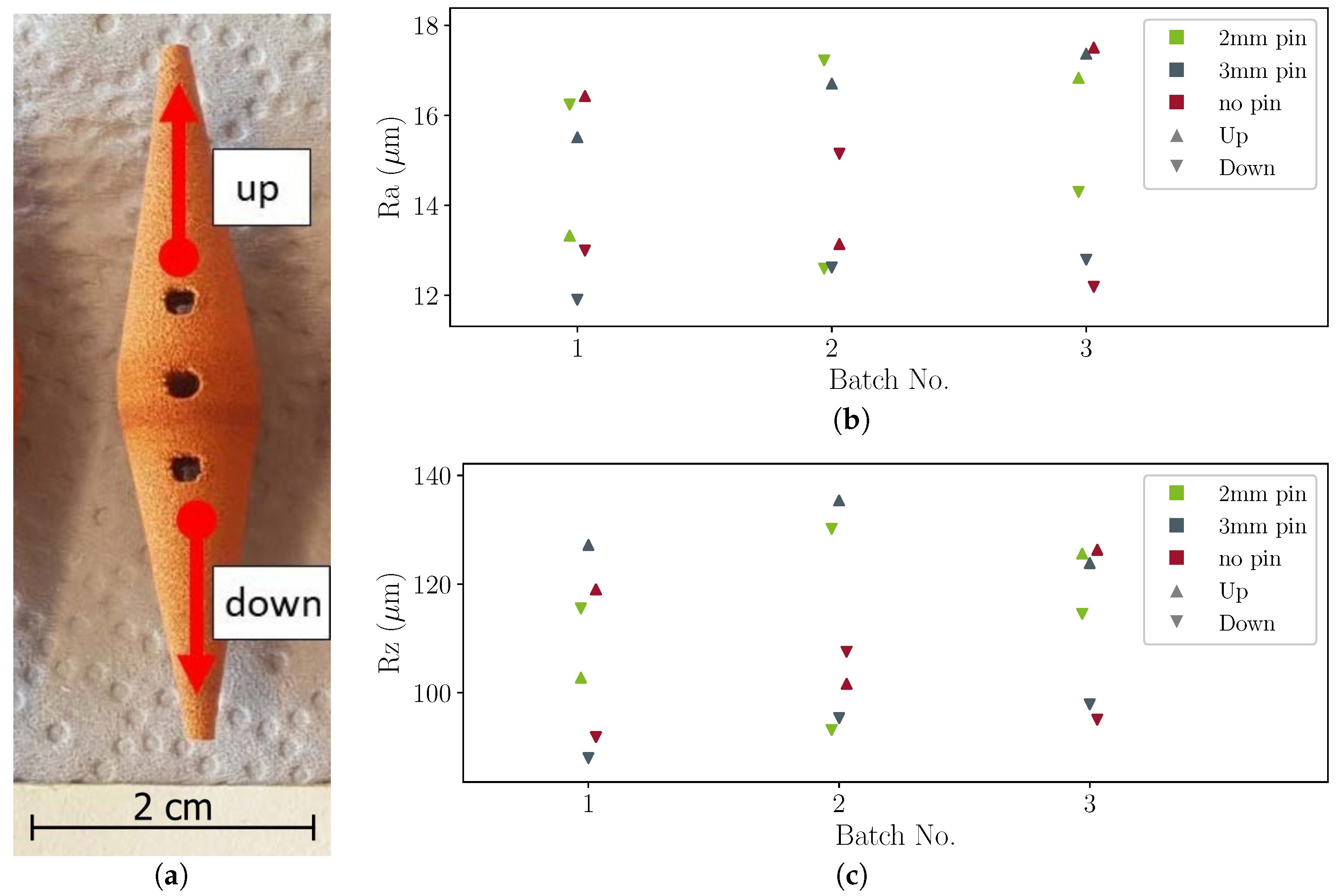
The surface roughness was measured using a Surfcom Touch 50 [26]. The probe diameter was 5 μm and the measurement was performed once for the upper cone and once for the lower cone of the collector for a distance of 8 mm, as shown in Figure 11a. The average profile height deviations from the mean line h ref , R a (see Equation (8)) [27], are shown in Figure 11a.
R a = 1 l 0 l h ( x ) h ref d x
The roughness ranges from 12 μm to 18 μm, with the topside being rougher than the lower part according to R a . Also, the maximum peak height to valley height R z (see Equation (9), Figure 11c) [27] indicates higher roughness on the upper side. Overall, the roughness of the 50 Ω geometry varies by ± 0.18 %, which is negligible.
R z = i = 1 n r p , i + r v , i n r p , i = max h ( x ) h ref , i x probe segment i r v , i = max h ref , i h ( x ) x probe segment i
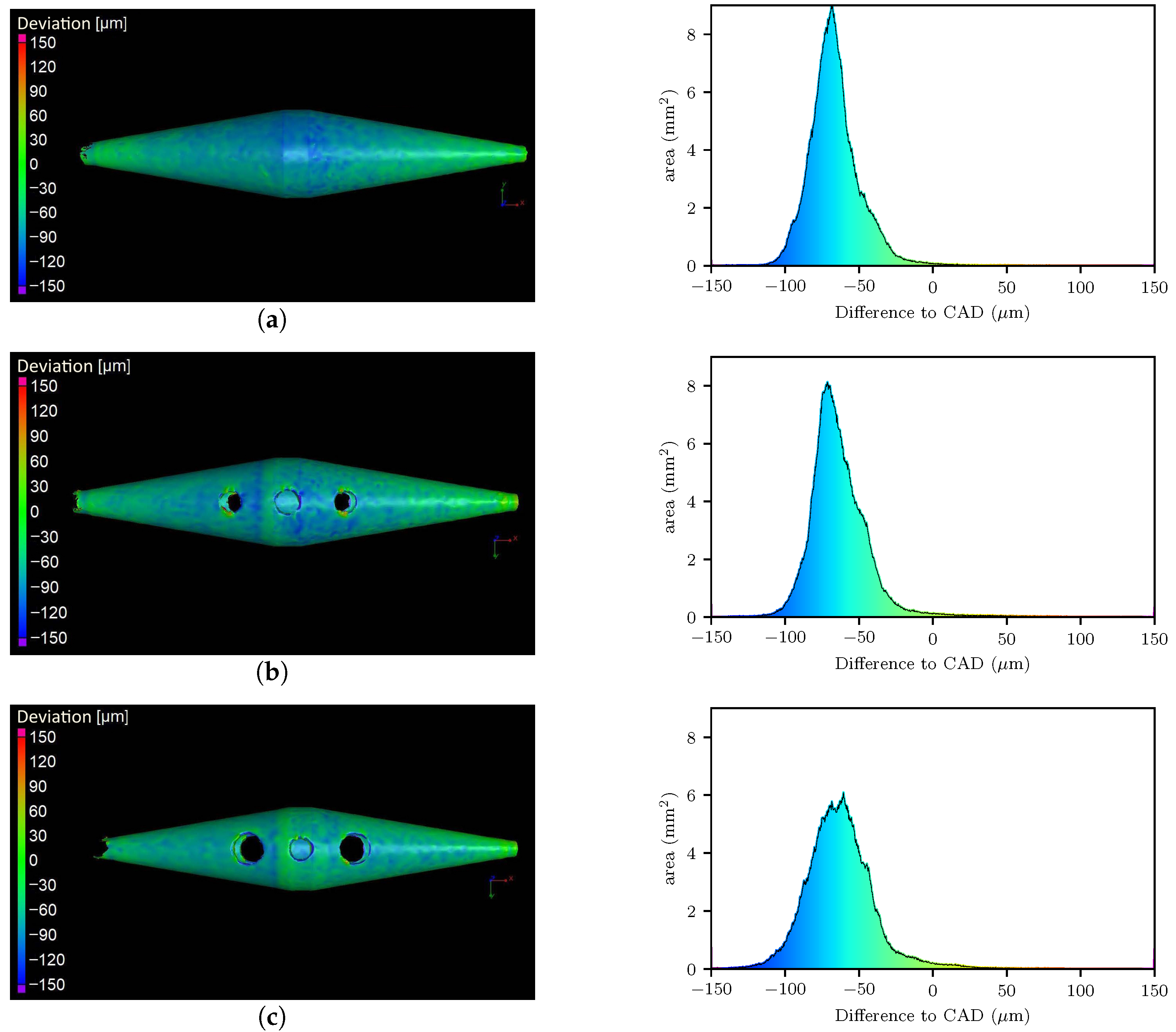
The deviation from the CAD model was measured using a GOM ATOS Core 135 and is shown in Figure 12. One challenge of additive manufacturing is the shrinkage of the body, which depends on the geometry and is difficult to predict. In our case, the shrinkage was about −20 μm to −100 μm, with the most common difference of 70  μm. This led to an error of 0.24% to 1.2% and most common 0.84 %. In future iterations, the collector geometries are planned to be additively manufractured with radii increased by approximately 50 μm to compensate for shrinkage, thereby reducing dimensional deviations and minimizing the impact on the 50 Ω geometry.
Another aspect of the surface roughness R a is its significant influence on the SEY. For random surfaces, the SEY first increases for R a < 0.3   μ m and decreases afterwards steadily with higher R a , as can be observed in Figure 10 of [28] for R a 1.6   μ m . Another study demonstrated that sputtering the surfaces with gold decreases the SEY, as shown in Figure 7 of [29] for a surface roughness R a of 0.25 μm to 1.5 μm. Since our surface roughness is higher by an order of magnitude, it remains unclear whether these results are directly applicable. The model of the reduction in the SEY described in [28,29] implies that produced SEs are recaptured in the valleys of the rough surfaces and thus do not contribute to the globally measured SEY. Hence, deeper valleys might be beneficial. Future work should also clarify whether these results transfer to very rough random surfaces. If so, additively manufacturing the chassis of the TRCFFC should reduce tertiary electrons, which are produced by electrons escaping the applied bias and finally hitting the chassis.

2.3. RF Characterization of the Radially Coupled FFC Designs

During the melting process in laser powder bed fusion (LPBF), small defects can occur, leading to porosity formation. The conductivity σ of the AM material is affected by this porosity, which adds up to other factors such as surface roughness and material impurity [30,31]. Additionally, the skin effect δ (Equation (10)) is affected, which plays a significant role in high frequency signal losses within conductors.
δ = 1 π f μ 0 μ r σ ,
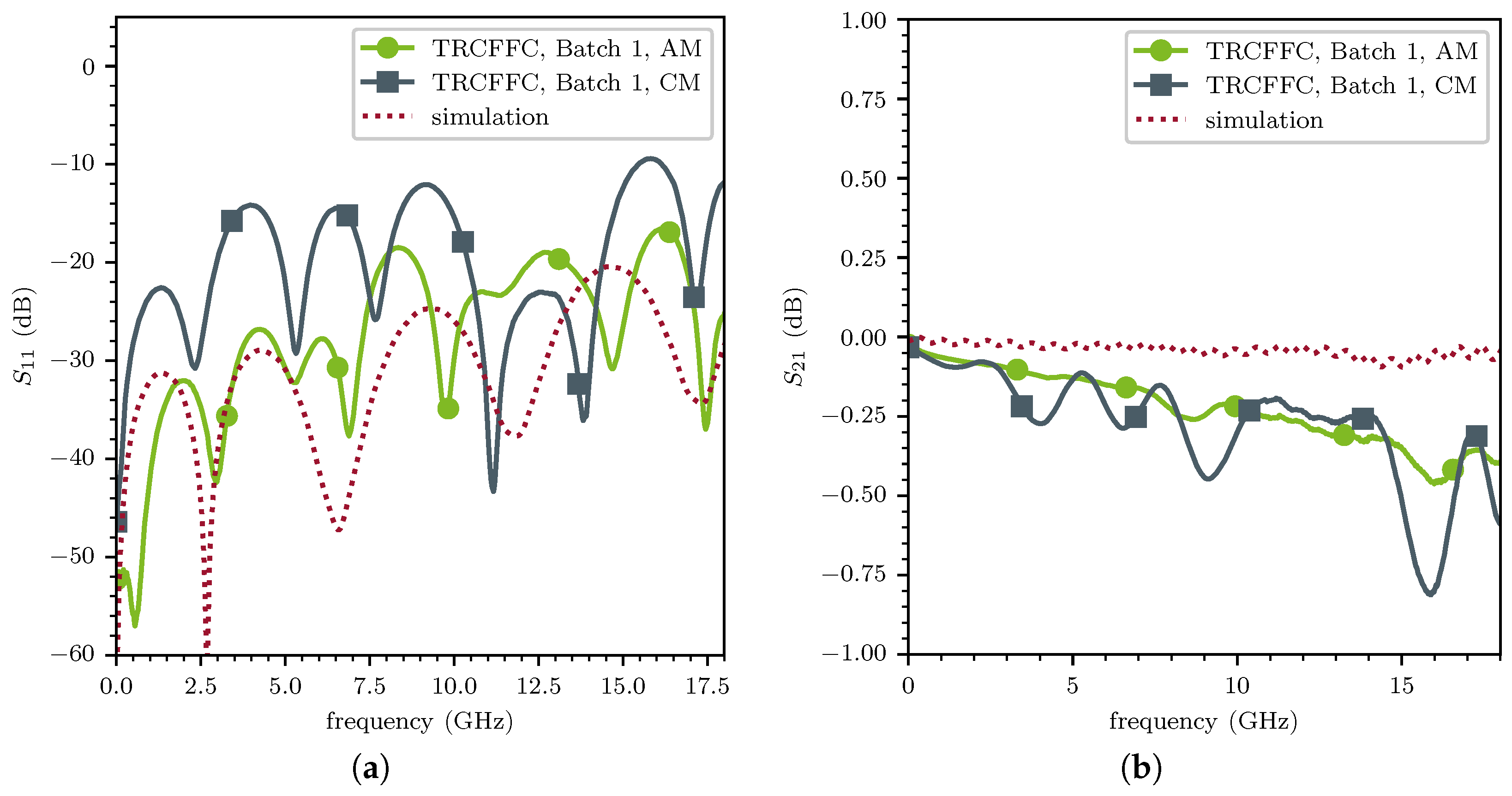
with the frequency f, the free space permeability μ 0 , the relative permeability μ r , and the electrical conductivity σ . For low-power lasers (e.g., 370 W), the conductivity of fused copper has been measured at approximately 58% to 73% of the international annealed copper standard (IACS) [30]. When high-power lasers (>500 W) are employed, conductivities of up to 94% [31] have been achieved. With a green laser, even an electrical conductivity of 100 IACS in the as-built condition is achievable [32]. Therefore, the RF properties of the TRCFFC are analyzed using both a conventionally machined (CM) and an AM collector. The primary figure of merit for the RF characterization are the S-parameters and the analysis of the temporal resolution, which was also compared to those obtained for the RCFFC. In Figure 13, the measured S-parameters for a CM and an AM collector are shown in comparison with the CST simulation results. These collectors have no holes for glass pins to study the differences in roughness and precision of the geometry apart from geometrically induced resonances. A FieldFox N9917A [33] with 0.5   m phase-stable SMA SUCOFLEX 126E cables [34] was used. The calibration was performed with a Keysight Ecal Module N7554A [35]. It is observed that the reflections (Figure 13a) are lower across nearly the entire 18 G Hz range, with the AM collector performing better, on average, by about 7.5 dB. Additionally, for the transmission (Figure 13b), there was improved performance across the entire measurement range, with an average of 0.05 dB. The deviation from the CAD model was measured using a VR-6000 [36] for both the traditionally machined and additively manufactured version seen in Figure 14. The measured profile were arranged to minimize the mean difference from the CAD model, resulting in smaller deviations compared to the previous full 3D scan in Figure 12. The mean difference for the AM version is 13 μ m and 37 μ m for the conventionally machined one. The surface roughness R a of 2.4   μ m of the CM collector is significantly smoother, but still, the geometrical differences are stronger than the differences in the roughness. Hence, the performance difference with respect to the S-parameter is dominated by the geometrical differences rather than the surface roughness.
In our case, the additively manufactured collectors exhibited geometrical deviations smaller than the conventionally machined ones, which was also reflected by the RF performance measurements. Therefore, we focused on these additively manufactured collectors to study the influence of the glass pins. Three different kinds of collectors were constructed, as shown in Figure 9: one without, one with 2 mm, and one with 3 mm holes for glass pins. The measurement results were compared with CST simulations across the full 18 G Hz bandwidth of the SMA connectors (see Figure 15). The best results were obtained without any glass nor holes for glass pins, as seen in Figure 15a. Adding 2 mm diameter holes to the collector did not affect the S-parameters up to 7.4   G Hz as seen in Figure 15b. However, the transmission was reduced above 7.4   G Hz to a minimum of 0.64 dB at 11.2   G Hz and the reflections increased up to 17 dB. Frequencies above 7.4   G Hz are, therefore, considered to be outside the bandwidth of the TRCFFC. After inserting 2 mm glass pins into the alignment hole, the S-parameters remained close to the previous results up to 7.4   G Hz (see Figure 15c). The transmission decreased for higher frequencies. The usage of the glass led to two absorption peaks at 14 G Hz and 16.8   G Hz . Increasing the diameter of the glass pins to 3 mm (see Figure 15d) leveled the reflection to 30 dB till 6 G Hz and quickly increased to 12 dB afterwards. The absorption caused by the thicker glass pins drastically broadened the absorption peak at 15.8   G Hz with a transmission of only 7 dB. Therefore, the use of glass should be minimized to lower the disturbance of the 50 Ω geometry still stabilizing the collector position in the tapered coaxial design. From the perspective of the S-parameters, this TRCFFC design with 2 mm glass pins could be used for bunches with a σ b 135   p s .
Concerning the coaxial design, the TRCFFC can be operated easily up to 7 G Hz , but the distance between the collector surface and the inner surface of the chassis also limits the usable bandwidth. The pre-field of the bunch advances ahead of the actual charges, prematurely reaching the collector and inducing a signal. This effect can be included into the calculation of the theoretical measurable bunch length σ c estimated by Equation (11) under the assumption that the diameter of the drill hole inside the collector and the drift tube after the heat shield is small compared to the distance L between the collector and the inner chassis surface [7]:
σ c 2 = σ b 2 + σ gap 2 .
where σ gap is the extension of the actual bunch length σ b and can be calculated from
σ gap = κ · L β · c 0 ,
with a geometrical constant κ = 0.30 [37] and the velocity β c 0 of the bunch. To evaluate this effect, a series of simulations with very short bunches at different velocities was performed. The resulting simulated signal of these very short bunches was equivalent to the impulse response of the FFCs. In Table 1, the resulting bunch length σ s of simulations for different bunch velocities β are shown next to the actual emitted bunch length σ b and the calculation of σ c . Thereby, we used the relation of the full width at half maximum FWHM = 2.3548 σ s to derive the bunch length from the output signal of the TRCFFC. Table 2 shows the results for the same simulation settings for the RCFFC. The temporal resolution σ TR is calculated from the emitted bunch length σ b and output signal σ s by σ TR = σ s 2 σ b 2 . The generation of SEs on the collector was activated to observe the effects of insufficient suppression, which led to longer measured bunches. The bias voltage was set to 0 V. In both tables, it is evident that the time of flight of the particles through the gap between the chassis and the collector is the dominant parameter for very short pulses (10 p s ). The higher β , the lower is the impact of σ gap , and hence, the precision of the FFC rises. In comparison to the RCFFC, the temporal resolution of the TRCFFC should be lower by a factor of 2.95 with respect to the theoretical model σ c . Examining the simulation results, the factor between the temporal resolution of both designs is estimated to a factor of 2.54. Increasing the diameter of the collector for the TRCFFC to improve the SE suppression results in a trade-off, as it comes at the cost of a lower bandwidth. However, as the bunch length increases, the deviation in the TRCFFC simulations for estimating the bunch length σ s at β = 15 % becomes less than 10% for bunch widths σ b exceeding σ b = 100   p s . For 400 ps, the deviation remains below 1% even without bias potential. The higher bandwidth of the RCFFC geometry results in a higher temporal resolution also for shorter bunches resulting in a lower deviation, e.g., 1.7 % for σ b = 100   p s at β = 15 % . Without an appropriate bias scheme, bunch shapes of σ b 400   p s are elongated. The lower temporal separation t sep of the RCFFC leads to an overlapping of the electron and ion signal resulting in a deviation of 17.5 % from the actual simulated bunch length. The finite temporal resolution at speed of light is 3.4   p s for the RCFFC and 5.3   p s for the TRCFFC.
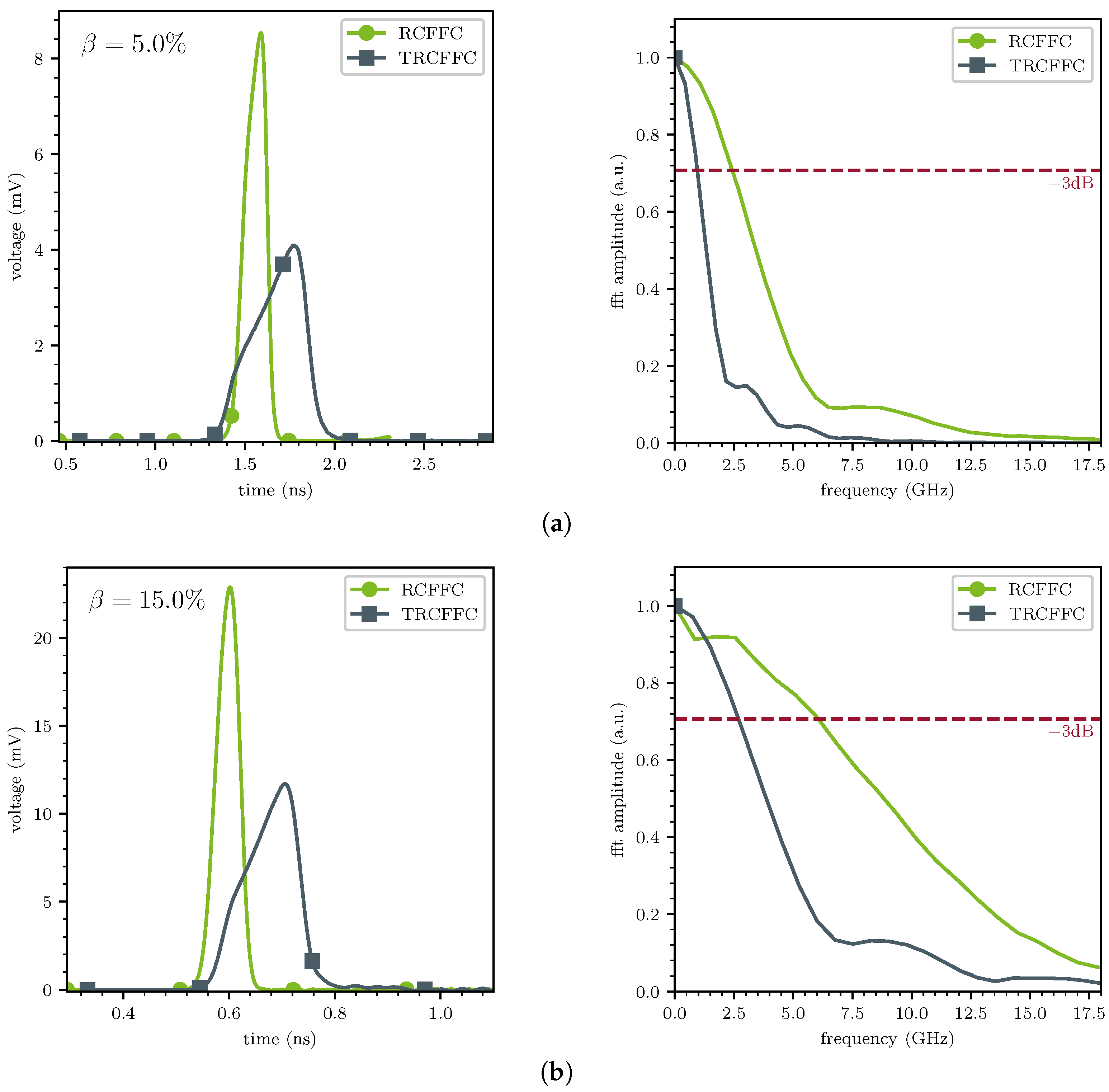
A second way to assess the temporal resolution is to estimate the 3 dB bandwidth of the FFCs. To do this, we simulated a very short pulse below the temporal resolution of the FFCs as shown in Figure 16 (left). For the desired design goal velocities, the lower bound was 5% and the upper one was 15%, which allowed us to obtain the impulse response of the systems. Then, we calculated the FFT of these signals (see Figure 16 right). The intersections of this amplitude signal with the level 0.707 is equivalent to 3 dB degradation in signal power. The bandwidth of the RCFFC at β = 5 % (see Figure 16a) is 2.432   G Hz (TRCFFC 0.953   G Hz ), and in the case of β = 15 % , the bandwidth is 6.064   G Hz (TRCFFC 2.685   G Hz ), which corresponds to a factor of 2.5 to 2.25 between the bandwidths of both devices. This is in line with the evaluation of the FWHM width estimation precision for very short bunches of 2.45 to 2.56 for the same velocity range, as discussed earlier in this section. Both methods for examining the temporal resolution capabilities show that radially coupled FFCs are beam velocity-dependent. Hence, they must be tailored to their use case in both expected velocities and bunch lengths.

2.4. Measurements

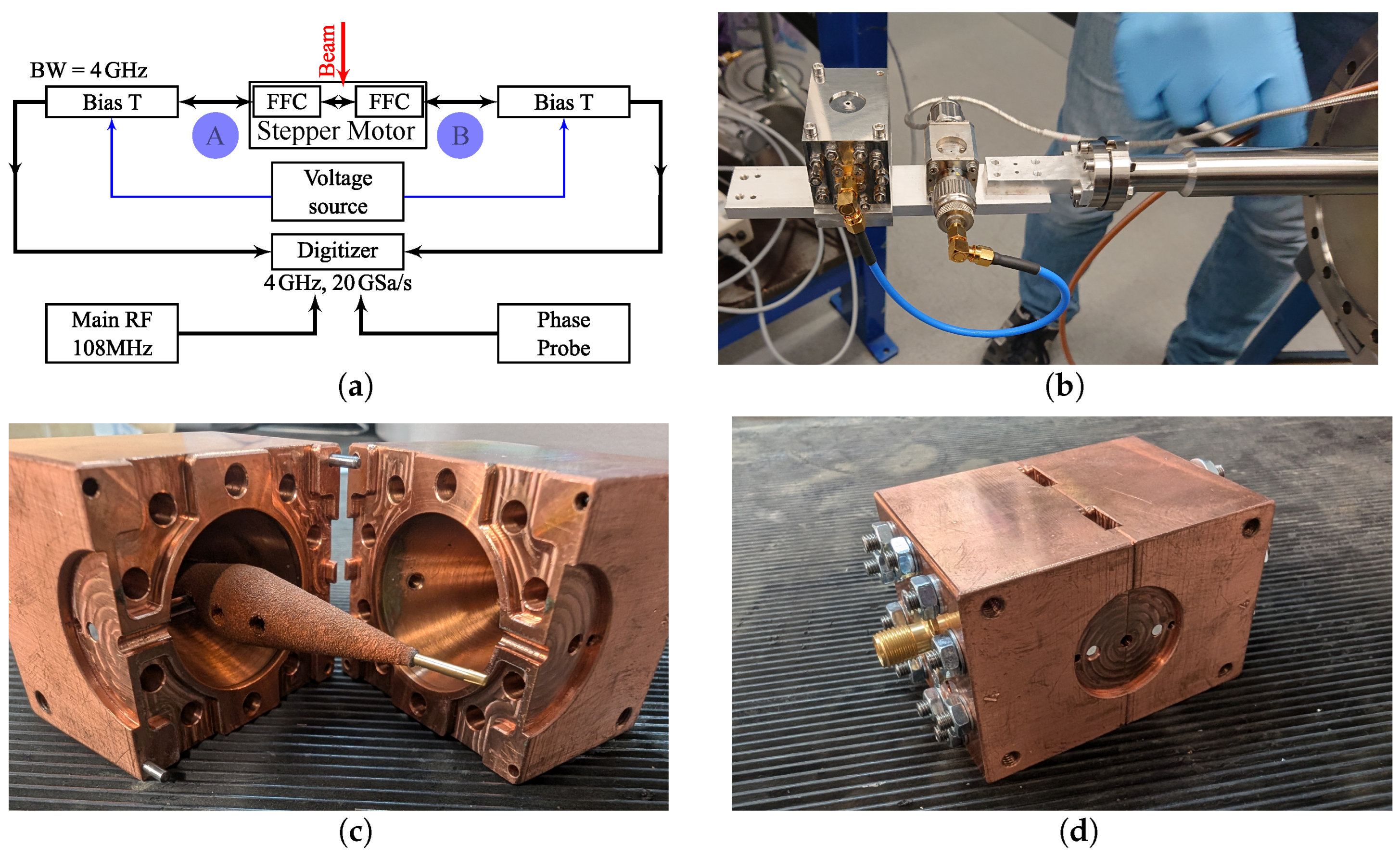
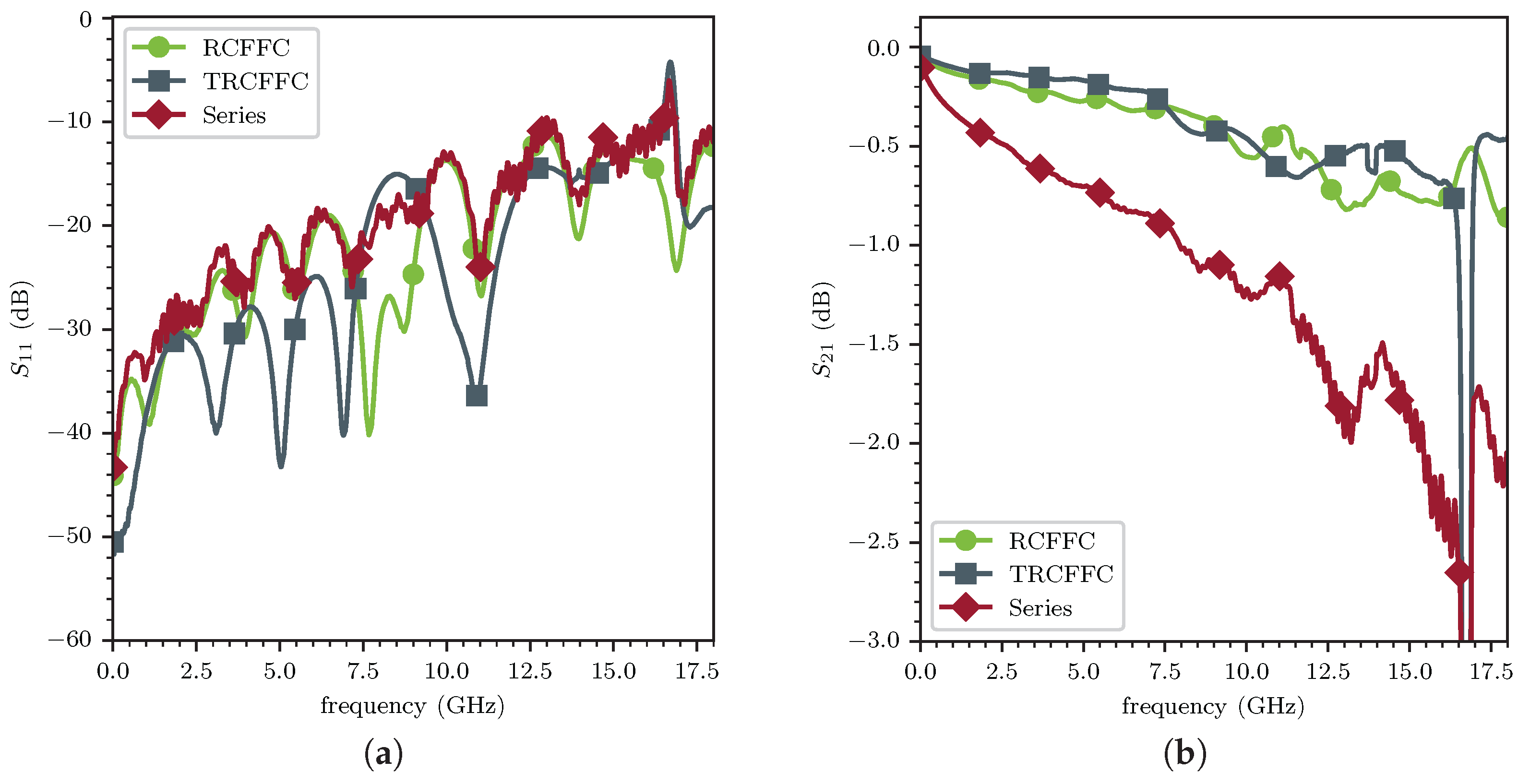
A measurement campaign was performed to compare the two radially coupled FFCs discussed above at the X2 measurement station at GSI. The measurements were performed with an Ar10+ beam at 11.4   M e V /u. Since there were only two vacuum feedthroughs available, RCFFC and TRCFFC were connected in series onto a stepper motor (see Figure 17b). Prior to the beam measurements, the RF properties were examined in terms of reflection and transmission of each single device and connected in a series as shown in Figure 18. The used RCFFC and TRCFFC performed similarly so that the combined reflection properties remained below 20 dB till 7 G Hz . The transmission was dominated by the additional 25 cm long SUCOFLEX 126E cable between them down to 0.8 dB till 7 G Hz . Using a shorter cable would further improve the transmission. So in each case, the other FFC behaved like a coaxial cable and did not affect the measurements.
The position of the FFCs was alterable in the horizontal plane by the stepper motor. The beam irradiated only one of the two FFCs at a given time. A measurement scheme with all the components is given in Figure 17a. The bias voltage was applied through Mini-Circuits ZX85-12G-S+ bias Tees [38] from both ports, ensuring that no DC current through the FFCs was induced. The signal was amplified with a broadband (low-noise) amplifier Mini-Circuits ZX60-14LN-S+ [39] and measured with a four-channel Lecroy WaveRunner 9404 [40] oscilloscope with 4 G Hz bandwidth and 20 GSa/s. In addition, the master RF signal of the UNILAC cavities was recorded to evaluate the bunch movements with respect to RF. The signal from the phase probe (PP) installed ≈0.9 m in front of the FFCs was also available for time of arrival triggering. An open, all-copper version of the TRCFFC can be seen in Figure 17c. The collector is arranged with a glass pin inside the chassis. The sealing RF surfaces are shown.
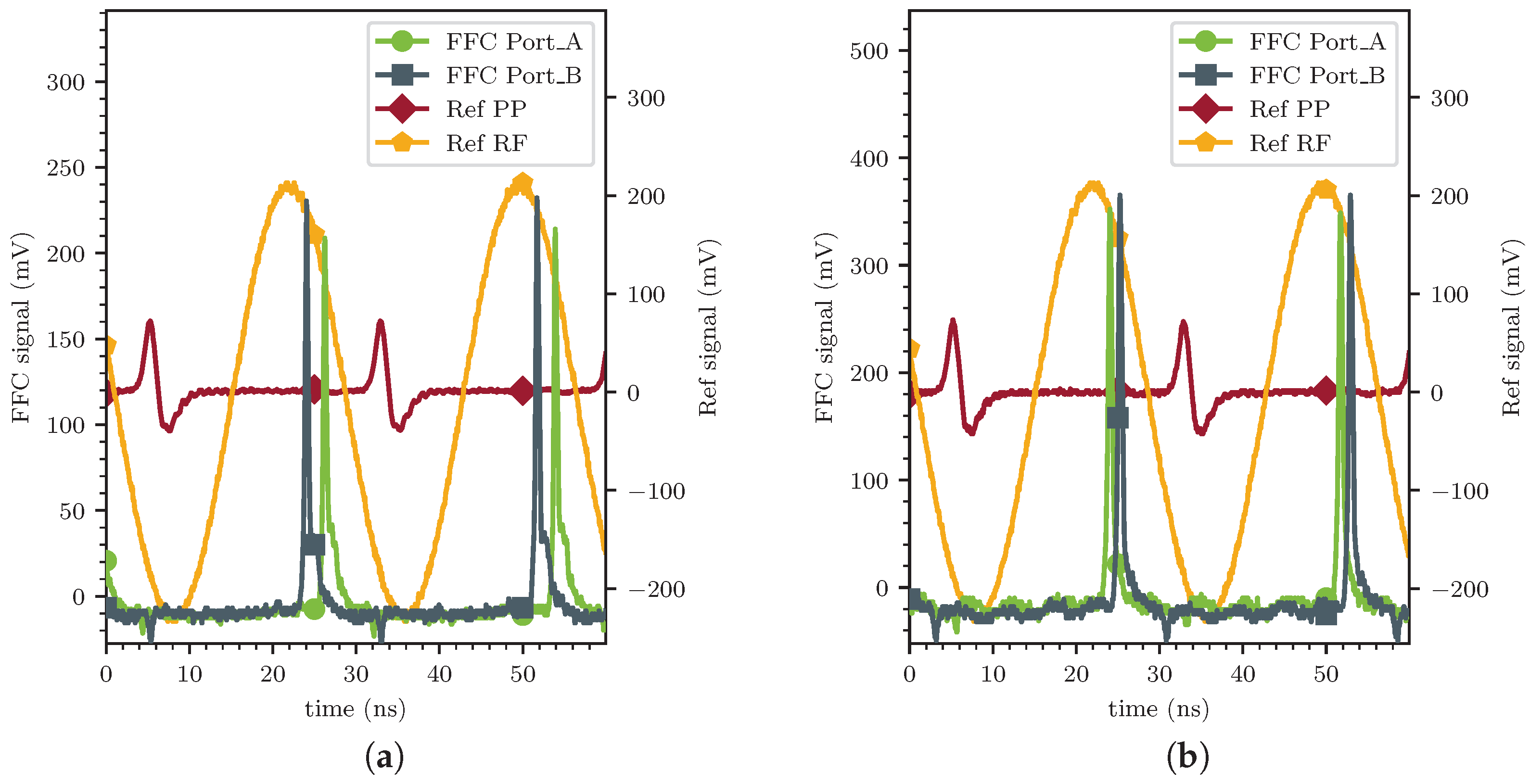
In Figure 19a,b, examples of two consecutive bunches within a macropulse measured with the RCFFC (left) and the TRCFFC (right) at the same position with respect to the beam axis without biasing are shown. The phase probe signal and reference RF are also marked. The time difference between the FFCs A and B ports is a result of different signal path lengths. The difference in the amplitude of the signals arises mainly due to the different damping from the additional cable between the FFCs and a small additional reflection of the second FFC. In line with the expectations, the amplitude of the ion peak of the TRCFFC is higher by a factor of 1.6 compared to the RCFFC. Furthermore, the tail of the SEs is lower and shorter in the TRCFFC due to the stronger geometrical SE suppression.
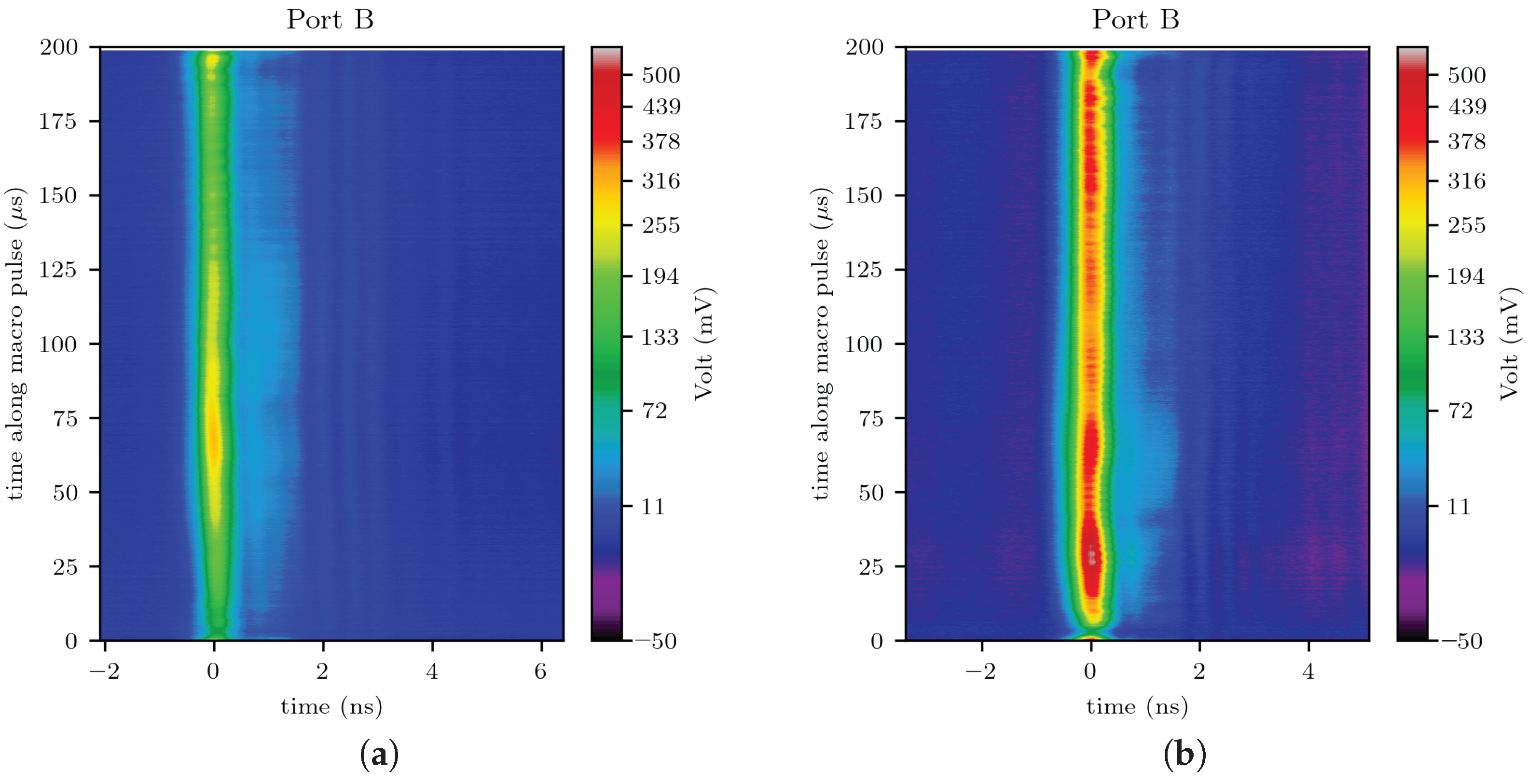
A full macropulse of about 7200 single bunches is shown in the waterfall diagram in Figure 20, aligned by the RF signal. While the amplitude of the ion peak changes significantly along the macropulse, no strong temporal jitter is observable. No bias voltage was applied to further suppress the SEs. Hence, a light blue tail is visible after the ion peak. This tail is 2 ns long for the RCFFC and 1 ns for the TRCFFC. The amplitude of the SE tail is slightly lower for the TRCFFC and, relative to the signal strength of the ion signal, lower by a factor of 2.
Due to the pinhole in the heat shield, the FFC selects only a 1.8 mm section in the case of the TRCFFC for typical beams with a transversal extension of about 10 mm in diameter. The most obvious effect is the change in the measured amplitude depending on whether the core of the beam or the outer regions are observed. The actual shape may alter with respect to the transverse–longitudinal position of the FFC due to position-dependent effects like dispersion. In Figure 21b, there is a second peak at 6.9   n s at an insertion depth of 16.25   c m , which was not observed at an insertion depth of 15.85   c m as shown in Figure 19 and Figure 20. A transversal sweep was performed with both FFCs through the beam. A plot of the average bunch shape of the full macropulse against the insertion depth position is shown in Figure 21. A bias of 25 V was applied during both measurements. With both FFCs, a preceding peak for insertion depths of 20.9 cm to 21.6 cm and 16.2 cm to 16.8 cm is observed. The X2 measurement station is connected to the exit of the UNILAC accelerating structure via a series of strong dipoles providing more than a 90 degree bend. Therefore, a large dispersion is expected to be present at the FFC location, although no beamline optics simulations are available. This large dispersion allows the radially coupled FFCs to sample the energy axis via its horizontal motion, and therefore, dispersion-assisted longitudinal emittance can be estimated as discussed in [41].
A horizontal sweep of the FFC was carried out in small steps to measure the bunch lengths. The resolution of this measurement depends on the hole size in the heat shield. Therefore, the finer pinhole of the RCFFC results in a finer measurement compared to the TRCFFC. In this measurement, the measured f gain between both types of FFCs can also be evaluated. The maximum intensity of the average bunch shape observed with the RCFFC is 68.07   m V , while the TRCFFC signal maximum is 145.25   m V . The measured f gain between both FFCs is 2.13, which roughly matches a beam width σ b , trans of 2.8   m m according to Equation (6). In Figure 21b, we see a reflection at 5.8   n s . This reflection is also visible in Figure 22a at 9 ns. A single mismatch likely occurred at a position approximately 0.6   m from the TRCFFC and 0.95   m from the RCFFC. Through the series configuration of the devices, this reflection appears in both measurements. Backtracking these distances to a common origin indicates the vacuum feedthrough of the beamline or the nearby attached bias tee outside the beamline as the most probable source of the reflection.
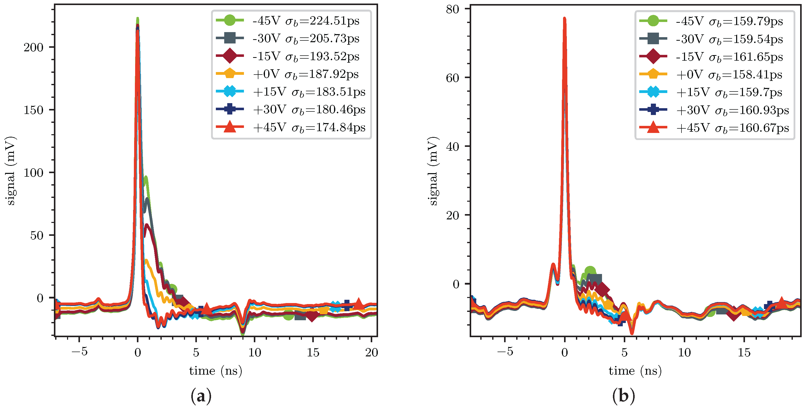
Finally, a bias voltage study was performed for both FFCs. The biasing scheme was applied at an insertion depth of 16.25   c m for the TRCFFC, while it was applied at an insertion depth of 20.65   c m for the RCFFC, where the second peak was not visible in the scan as shown in Figure 21a. To emphasize the difference in the geometrical SE suppression of both designs, the bunch shape along the macropulse in Figure 22 was averaged for different bias voltages ranging from −45 V to 45 V. The bunch width σ b was estimated using the FWHM divided by 2.3548. If the bias voltage is sufficiently high, the bunch length estimation stabilizes at a certain value, even if the bias voltage is increased further. The estimated bunch length changed from 224.5 p s to 174.8 p s depending on the used bias for the RCFFC. The temporal separation and the geometrical suppression were not strong enough to suppress the SEs without a bias. A higher bias would be necessary for an accurate estimation. In contrast, the bunch width estimated with the TRCFFC ranged from 159.8 p s to 160.9 p s at the insertion position of 16.25   c m . Even a high negative bias had no severe impact on the estimated σ b . Hence, the bunch length estimation can be considered to be accurate with an average bunch length over all bias measurements of 160.1 ± 0.4   p s .

3. Summary

This study presented the design, simulation, and experimental validation of Fast Faraday Cups with an emphasis on a newly developed tapered radially coupled FFC. The primary objective was to improve the suppression of SEs and to enhance the signal-to-noise ratio for bunch-by-bunch measurements.
The comparative simulations and RF characterizations of axially and radially coupled FFCs revealed that radial coupling, when combined with a deep, conical drill hole geometry in the collector, provides superior SE suppression. This geometrical approach allowed effective decoupling of the SE signals from the primary ion-induced signal, which reduced temporal overlap. The TRCFFC design exhibited a geometrical reduction in SEs down to 2.4 % of all the emitted SEs and can temporally separate 99% of the SE signal from a bunch with a width of σ b = 400   p s even without biasing. In general, a bias should be applied and is especially foreseen for high charge state ions.
Additive manufacturing has proven to be highly suitable for fabricating FFC collectors, enabling their successful application in this diagnostic application. Despite slight dimensional deviations and moderate surface roughness, AM copper collectors achieved excellent RF performance. The simulations and S-parameter measurements further confirmed that, even after adding alignment glass pins, the operational bandwidth remained sufficient (up to 7 G Hz ) for the TRCFFC. Though the geometry of the TRCFFC is relatively simple, complex substructures such as cooling channels for high-current FFC can significantly enhance their capabilities [42]. Furthermore, it is important to study how the surface properties of AM parts influence the generation of SEY, especially for rough random surfaces.
The experimental measurements at the GSI UNILAC further validated the performance. The TRCFFC provided higher signal amplitudes by a factor ≈ 2.13 compared to the RCFFC and showed shorter SE tails. In case of an Ar10+ at 11.4   M e V /u, the measured bunch length remained stable at 160 p s for various bias settings, while the RCFFC showed a significant dependency on the bias voltage, which indicates an insufficient SE suppression under these circumstances. The use case for the RCFFC are high-bandwidth-driven measurements above 3 G Hz bandwidth and measurements of slower bunches ( 10 %   c 0 ) because of the β dependency of the temporal resolution of radially coupled FFCs. Additionally, horizontal scans through the beam showed that the radially coupled FFCs could detect spatial variations in the bunch structure, which can be caused by, e.g., dispersion. The ability to perform dispersion-assisted longitudinal emittance measurements with radially coupled FFCs could be a useful and fast longitudinal emittance measurement technique. Using the FFCs, further secondary electron emission spectra and yield could also be studied.

Author Contributions

S.K. and R.S. contributed to the conception, simulations, measurements, and writing of the manuscript. S.G. additively manufractured the TRCFFC collectors and performed the roughness measurements. L.S., A.P. and H.D.G. reviewed the manuscript. All authors have read and agreed to the published version of the manuscript.

Funding

This work is supported by the German Federal Ministry of Research, Technology and Space (BMFTR) under contract no. 05P21RORB2. Joint Project 05P2021—R&D Accelerator (DIAGNOSE).

Institutional Review Board Statement

Not applicable.

Data Availability Statement

The data presented in this study are available upon request from the corresponding author.

Acknowledgments

We acknowledge the help from GSI colleague Michael Mueller for his help in construction and assembly of the TRCFFCs and GSI mechanical workshop for manufacturing the FFC body and roughness measurements.

Conflicts of Interest

The funders had no role in the design of the study; in the collection, analyses, or interpretation of data; in the writing of the manuscript; or in the decision to publish the results.

References

  1. Carneiro, J.-P.; Hanna, B.; Podzeyev, E.; Prost, L.; Saini, A.; Shemyakin, A. Longitudinal Beam Dynamics Studies at the PIP-II Injector Test Facility. Int. J. Mod. Phys. A 2019, 34, 1942013. [Google Scholar] [CrossRef]
  2. Rawnsley, W.R.; Laxdal, R.E.; Root, L.; Mackenzie, G.H. Bunch Shape Measurements Using Fast Faraday Cups and an Oscilloscope Operated by LabVIEW over Ethernet. AIP Conf. Proc. 2000, 546, 547–554. [Google Scholar] [CrossRef]
  3. Bogaty, J.M.; Clifft, B.E.; Pardo, R.C. A Very Wide Bandwidth Faraday Cup Suitable for Measuring Gigahertz Structure on Ion Beams with Velocities Down to <0.01. In Proceedings of the Linear Accelerator Conference (LINAC’90), Albuquerque, NM, USA, 10–14 September 1990; JACoW Publishing: Geneva, Switzerland, 1990; pp. 465–467. Available online: https://jacow.org/l90/papers/TU457.pdf (accessed on 30 July 2025).
  4. Strehl, P. Beam Instrumentation and Diagnostics; Particle Acceleration and Detection Series; Springer: Berlin/Heidelberg, Germany, 2006; ISBN 3-540-26401-9. [Google Scholar] [CrossRef]
  5. Ferianis, M.; Bassanese, S.; D’Auria, G. Characterisation of Fast Faraday Cups at the ELETTRA Linac. In Proceedings of the 6th European Workshop on Beam Diagnostics and Instrumentation for Particle Accelerators (DIPAC 2003), Mainz, Germany, 5–7 May 2003; p. 113. Available online: https://cds.cern.ch/record/923942 (accessed on 30 July 2025).
  6. Mathew, J.V.; Bajaj, A. An Improved Strip-Line Fast Faraday Cup for Beam Bunch Measurements. Rev. Sci. Instrum. 2020, 91, 113305. [Google Scholar] [CrossRef] [PubMed]
  7. Mal, K.; Kumar, S.; Rodrigues, G.; Singh, R. Study and Improvements of a Radially Coupled Coaxial Fast Faraday Cup Design Toward Lower Intensity Beams. AIP Adv. 2022, 12, 125223. [Google Scholar] [CrossRef]
  8. Jackson, J.D. Classical Electrodynamics, 3rd ed.; Wiley: New York, NY, USA, 1999; ISBN 0-471-30932-X. [Google Scholar]
  9. Masoumzadeh, A.; Habibi, M.; Afsharmanesh, M. Design, construction and test of an optimized Faraday cup for beam current determination of a helicon ion source. Vacuum 2019, 159, 99–104. [Google Scholar] [CrossRef]
  10. Dassault Systèmes. CST Studio Suite. Available online: https://www.3ds.com/products/simulia/cst-studio-suite (accessed on 30 July 2025).
  11. Fujimoto, T.; Iida, T.; Sumita, K.; Taniguchi, R. Fast response Faraday cup for low-energy, nanosecond-pulse ion beams. Rev. Sci. Instrum. 1982, 53, 168–170. [Google Scholar] [CrossRef]
  12. Chuaqui, H.; Favre, M.; Wyndham, E.S.; Arroyo, L.; Choi, P. Simple Faraday cup with subnanosecond response. Rev. Sci. Instrum. 1989, 60, 141–142. [Google Scholar] [CrossRef]
  13. Singh, R.; Klaproth, S.; Forck, P.; Reichert, T.; Reiter, A. Simulation and Measurements of the Fast Faraday Cups at GSI UNILAC. In Proceedings of the 11th International Beam Instrumentation Conference (IBIC 2022), Kraków, Poland, 5–9 September 2022; pp. 286–290. [Google Scholar] [CrossRef]
  14. Sternglass, E.J. Theory of Secondary Electron Emission by High-Speed Ions. Phys. Rev. 1957, 108, 1–12. [Google Scholar] [CrossRef]
  15. Rothard, H.; Kroneberger, K.; Clouvas, A.; Veje, E.; Lorenzen, P.; Keller, N.; Kemmler, J.; Meckbach, W.; Groeneveld, K.O. Secondary-Electron Yields from Thin Foils: A Possible Probe for the Electronic Stopping Power of Heavy Ions. Phys. Rev. A 1990, 41, 2521–2535. [Google Scholar] [CrossRef] [PubMed]
  16. Koyama, A.; Shikata, T.; Sakairi, H. Secondary Electron Emission from Al, Cu, Ag and Au Metal Targets under Proton Bombardment. Jpn. J. Appl. Phys. 1981, 20, 65–70. [Google Scholar] [CrossRef]
  17. Hasselkamp, D.; Lang, K.G.; Scharmann, A.; Stiller, N. Ion Induced Electron Emission from Metal Surfaces. Nucl. Instrum. Methods 1981, 180, 349–356. [Google Scholar] [CrossRef]
  18. Reiter, A.; Witthaus, M.; Löchner, S.; Frühauf, J. Investigation of Cross Talk in Secondary Electron Emission Grids; Technical Note LOBI-TN-SEM-2012-001; GSI: Darmstadt, Germany, 2012. [Google Scholar]
  19. Benka, O.; Schinner, A.; Fink, T.; Pfaffenlehner, M. Electron-emission yield of Al, Cu, and Au for the impact of swift bare light ions. Phys. Rev. A 1995, 52, 3959–3965. [Google Scholar] [CrossRef] [PubMed]
  20. Haque, A.K.F.; Haque, M.M.; Sultana, S.; Patoary, M.A.R.; Hossain, M.S.; Maaza, M.; Uddin, M.A. Proton-Induced Secondary Electron Emission from Elemental Solids over the Energy Domain 1 keV–1000 MeV. Results Phys. 2019, 15, 102519. [Google Scholar] [CrossRef]
  21. Hasselkamp, D.; Rothard, H.; Groeneveld, K.O.; Kemmler, J.; Varga, P.; Winter, H. Particle Induced Electron Emission 2; Springer: Berlin/Heidelberg, Germany, 1992; Volume 4, p. 25. [Google Scholar]
  22. Ziegler, J.F.; Ziegler, M.D.; Biersack, J.P. SRIM—The Stopping and Range of Ions in Matter (2013 Version). Available online: http://www.srim.org/SRIM/SRIMLEGL.htm (accessed on 30 July 2025).
  23. Barth, W.; Scheeler, U.; Vormann, H.; Miski-Oglu, M.; Vossberg, M.; Yaramyshev, S. High brilliance beam investigations at the universal linear accelerator. Phys. Rev. Accel. Beams 2022, 25, 040101. [Google Scholar] [CrossRef]
  24. Skaritka, J.; Antipov, S.; Jing, C.; Neveu, N. Beam Instrumentation and Diagnostic Devices and Methods. U.S. Patent US20220039246A1, 3 February 2022. Available online: https://patents.google.com/patent/US20220039246A1/en (accessed on 30 July 2025).
  25. Ruggiero, A.G.; Rochlitz, S.S. Split-Structure Particle Accelerators. Patent 10932354, 23 February 2021. Available online: https://trea.com/information/split-structure-particle-accelerators/patentgrant/8349f7d8-42eb-4f53-b84f-a6c1673b2255 (accessed on 30 July 2025).
  26. ACCRETECH. SURFCOM TOUCH 50—Roughness Measuring System. Available online: https://www.accretech.eu/en/surface-measuring-systems/roughness-measuring-systems/surfcom-touch-50/ (accessed on 30 July 2025).
  27. DIN 4768; Determination of Surface Roughness Parameters Ra, Rz, Rmax Using Electrical Contact (Stylus) Instruments. German Institute for Standardization (DIN): Berlin, Germany, 1990.
  28. Cao, M.; Zhang, N.; Hu, T.; Wang, F.; Cui, W.-Z. Secondary electron emission from rough metal surfaces: A multi-generation model. J. Phys. D Appl. Phys. 2015, 48, 055501. [Google Scholar] [CrossRef]
  29. Peng, M.; Lin, S.; Zhang, C.; Liang, H.; Liu, C.; Cao, M.; Hu, W.; Zhai, Y.; Li, Y. Effect of the Surface Morphology of Porous Coatings on Secondary Electron Yield of Metal Surface. Materials 2022, 15, 4322. [Google Scholar] [CrossRef] [PubMed]
  30. Robinson, J.; Munagala, S.P.; Arjunan, A.; Simpson, N.; Jones, R.; Baroutaji, A.; Govindaraman, L.T.; Lyall, I. Electrical Conductivity of Additively Manufactured Copper and Silver for Electrical Winding Applications. Materials 2022, 15, 7563. [Google Scholar] [CrossRef] [PubMed]
  31. Jadhav, S.D.; Goossens, L.R.; Kinds, Y.; Vanmeensel, K.; Kruth, J.-P.; Van Hooreweder, B. Laser-Based Powder Bed Fusion Additive Manufacturing of Pure Copper. Addit. Manuf. 2021, 42, 101990. [Google Scholar] [CrossRef]
  32. Gruber, S.; Stepien, L.; López, E.; Brueckner, F.; Leyens, C. Physical and Geometrical Properties of Additively Manufactured Pure Copper Samples Using a Green Laser Source. Materials 2021, 14, 3642. [Google Scholar] [CrossRef] [PubMed]
  33. Keysight. FieldFox A-Series Handheld Analyzers, Model N9917A Datasheet; Keysight Technologies: Santa Rosa, CA, USA, 2024; Available online: https://www.keysight.com/de/de/assets/7018-03314/data-sheets/5990-9783.pdf (accessed on 30 July 2025).
  34. Huber+Suhner. SF126 Coaxial Cable Datasheet. Available online: https://www.mouser.de/datasheet/2/829/Huber_Suhner_10242018_SF126-1489558.pdf (accessed on 30 July 2025).
  35. Keysight. N7554A Electronic Calibration Module (ECal), DC to 18 GHz, 2-Port; Keysight Technologies: Santa Rosa, CA, USA, 2024; Available online: https://www.keysight.com/us/en/product/N7554A/electronic-calibration-module-ecal-dc-18-ghz-2-port.html (accessed on 30 July 2025).
  36. Keyence. VR-6000 Series Wide-Area 3D Measurement System; Keyence Corporation: Osaka, Japan, 2024; Available online: https://www.keyence.de/products/3d-measure/roughness-measure/vr-6000/ (accessed on 30 July 2025).
  37. Fermilab. Estimation of Dilution of a Fast Faraday Cup Response Due to the Finite Particles Speed. In FERMILAB-TM-2641-AD: Beam Diagnostics and Instrumentation; Fermilab: Batavia, IL, USA, 2016. Available online: https://lss.fnal.gov/archive/test-tm/2000/fermilab-tm-2641-ad.pdf (accessed on 30 July 2025).
  38. Mini-Circuits. ZX85-12G-S+ Datasheet; Mini-Circuits: Brooklyn, NY, USA, 2024; Available online: https://www.minicircuits.com/pdfs/ZX85-12G-S+.pdf (accessed on 30 July 2025).
  39. Mini-Circuits. ZX60-14LN-S+ Datasheet; Mini-Circuits: Brooklyn, NY, USA, 2024; Available online: https://www.minicircuits.com/pdfs/ZX60-14LN-S+.pdf (accessed on 30 July 2025).
  40. Teledyne LeCroy. WaveRunner 9000 Series Oscilloscopes Datasheet; Teledyne LeCroy: Chestnut Ridge, NY, USA, 2024; Available online: https://cdn.teledynelecroy.com/files/pdf/waverunner9000-datasheet.pdf (accessed on 30 July 2025).
  41. Singh, R. Longitudinal beam diagnostics R&D at GSI-UNILAC. In Proceedings of the HIAT 2022, Darmstadt, Germany, 27 June–1 July 2022. [Google Scholar] [CrossRef]
  42. Romano, T.; Arnold, N.; Kasemir, K.; Andresen, T.; Garion, C. Metal additive manufacturing for particle accelerator applications. Phys. Rev. Accel. Beams 2024, 27, 054801. [Google Scholar] [CrossRef]
Figure 1. Cross section view of an (a) axially coupled FFC [2] and (b) a radially coupled FFC [1]. All geometrical dimensions are given in m m .
Instruments 09 00032 g001
Figure 2. CST PIC simulation of the ACFFC (Figure 1a) with σ b = 100   p s and different bias settings with activated SEE.
Instruments 09 00032 g002
Figure 3. CST PT simulations of the ACFFC (top) and radially coupled Fast Faraday Cup (RCFFC) (bottom) for the bias settings 50 V (a,d), 50 V (b,e) and 250 V (c,f). The incoming ions are shown in red and the emitted SEs are blue. The equipotential lines of the bias field are overlayed to the actual geometry of the FFCs close to the collector surfaces.
Instruments 09 00032 g003
Figure 4. CST PIC simulations of the RCFFC (Figure 1b) with different bias settings and bunch lengths (a) σ b = 100   p s and (b) σ b = 400   p s with activated SEE.
Instruments 09 00032 g004
Figure 5. Temporal separation of the SE peak from the ion peak for different long drill holes and bunch lengths. In addition, the fraction of SEs of the gamma distribution for T e = 10   e V above the respective kinetic energy E kin is shown as a dashed line.
Instruments 09 00032 g005
Figure 6. Cross section of a TRCFFC with optimized geometrical SE suppression highlighting the copper collector (red dashed line), the quartz glass pins (blue cross-hatched), and the tantalum heat shield (purple dashed line). Angles are given in °, and all other geometrical dimensions in m m .
Instruments 09 00032 g006
Figure 7. CST PT simulations of the TRCFFC for the bias settings 50 V (a), 50 V (b), and 250 V (c). The incoming ions are shown red and the emitted SEs are blue. The equipotential lines of the bias field are overlayed to the actual geometry of the FFC close to the collector surfaces.
Instruments 09 00032 g007
Figure 8. CST PIC simulations of the TRCFFC (see Figure 6) with different bias settings and bunch lengths (a) σ b = 100   p s and (b) σ b = 100   p s with activated SEE.
Instruments 09 00032 g008
Figure 9. AM collectors on the printing bed first batch (a) and third batch (b).
Instruments 09 00032 g009
Figure 10. Collectors after cleaning from the powder, first batch (a), and third batch (b). The arrow marks the printing direction.
Instruments 09 00032 g010
Figure 11. (a) Measurement of the surface roughness starting from two points with a probe diameter of 5 μm on a length of 8 mm upwards and downwards, (b) shows the measured average profile height deviations from the mean line R a , and (c) the maximum peak height to valley height R z .
Instruments 09 00032 g011
Figure 12. Three-dimensional scan of the AM collectors of batch 3 with color-coded difference to the CAD model for the geometries (a) no glass pins, (b) 2 m m glass pins, and (c) 3 m m glass pins. On the right-hand side, the corresponding histograms display the distribution of these differences in terms of surface area using the same color coding as the 3D scans.
Instruments 09 00032 g012
Figure 13. S-parameter (a) S 11 and (b) S 21 measured using a TRCFFC chassis with 2 m m holes for glass pins and collectors without alignment holes. One collector was additively manufactured (AM) and the other conventionally machined (CM).
Instruments 09 00032 g013
Figure 14. Three-dimensional scan of the difference to the CAD model for the AM (a) and the CM (b) version of the collector. On the right-hand side, the corresponding histograms display the distribution of these differences in terms of count of measurements, using the same color coding as the 3D scans.
Instruments 09 00032 g014
Figure 15. S-parameters of different designs: (a) TRCFFC with collector without holes for glass pins, (b) TRCFFC with collector with 2 m m holes for glass pins, (c) TRCFFC with collector with inserted 2 m m thick glass pins, (d) TRCFFC with collector with inserted 3 m m thick glass pins.
Instruments 09 00032 g015
Figure 16. CST HFTD simulation of a σ b = 10   p s bunch for velocities β (a) 5% and (b) 15%, for the RCFFC and TRCFFC geometries (left). The corresponding FFT of the simulated signals (right) shows the 3 dB bandwidth, marked by the dashed line.
Instruments 09 00032 g016
Figure 17. Experimental setup in the GSI experimental cave X2: (a) scheme of the signal paths and (b) installation of the RCFFC and the TRCFFC on a stepper motor. Assembly of a full copper version of the TRCFFC with open chassis (c) demonstrating the positioning of the collector using a glass pin and the closed chassis (d).
Instruments 09 00032 g017
Figure 18. Measured S 11 (a) and S 21 (b) of a RCFFC and a TRCFFC seperately and installed in a series circuit.
Instruments 09 00032 g018
Figure 19. Two example measurements showing the phase probe and RF reference signal together with the measured signals of port A and B using (a) RCFFC and (b) TRCFFC as measurement devices with an Ar10+ beam at 11.4 M e V /u.
Instruments 09 00032 g019
Figure 20. Waterfall diagram of a full macropulse (about 7200 single bunches) of an Ar10+ beam at 11.4 MeV/u in the experimental cave X2 of GSI measured with (a) RCFFC (position 20.65 c m ) and (b) TRCFFC (position 15.85 c m ) without biasing.
Instruments 09 00032 g020
Figure 21. Waterfall diagram of the average signal of the macro pulse at different insertion positions measured with an Ar10+ beam at 11.4 M e V /u in the experimental cave X2 of GSI using (a) RCFFC and (b) TRCFFC suppression the SEs with a bias voltage of 25 V .
Instruments 09 00032 g021
Figure 22. Average signal of the macro pulse applying different bias voltages measured with an Ar10+ beam at 11.4 M e V /u in the experimental cave X2 of GSI using (a) RCFFC (position 20.65 m m ) and (b) TRCFFC (position 16.25 m m ). In addition, the bunch length σ b is stated as calculated from the FWHM.
Instruments 09 00032 g022
Table 1. Timings of TRCFFC.
Beam Velocity β (%) σ b   p s σ c p s σ s p s Temporal Resolution σ TR   p s
110650.53746.39746.32
510130.47146.85146.51
151044.5050.8349.84
15100109.00110.8647.85
15400402.34402.9949.03
251027.8732.7831.22
Table 2. Timings of RCFFC.
Beam Velocity β (%) σ b   p s σ c p s σ s p s Temporal Resolution σ TR   p s
110210.38300.75300.58
51043.2060.9060.07
151017.2121.8319.40
15100100.98101.7518.79
15400400.25470.87248.43
251013.0615.0311.22
Disclaimer/Publisher’s Note: The statements, opinions and data contained in all publications are solely those of the individual author(s) and contributor(s) and not of MDPI and/or the editor(s). MDPI and/or the editor(s) disclaim responsibility for any injury to people or property resulting from any ideas, methods, instructions or products referred to in the content.