
Fabrication and First Full Characterisation of Timing Properties of 3D Diamond Detectors

 , , ,
, , ,  and
and 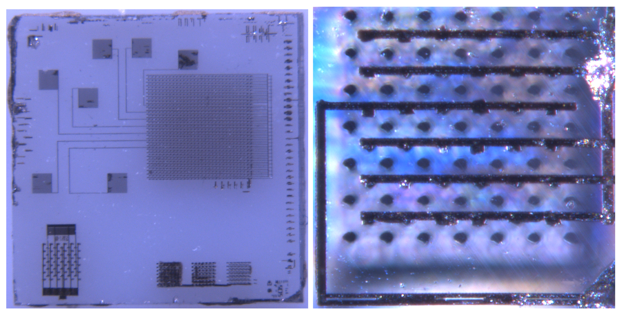
Abstract
1. Introduction
2. Sensor Fabrication
2.1. Fabrication of First Prototype Sensor
2.2. Fabrication of New Sensors
3. Sensor Test Results
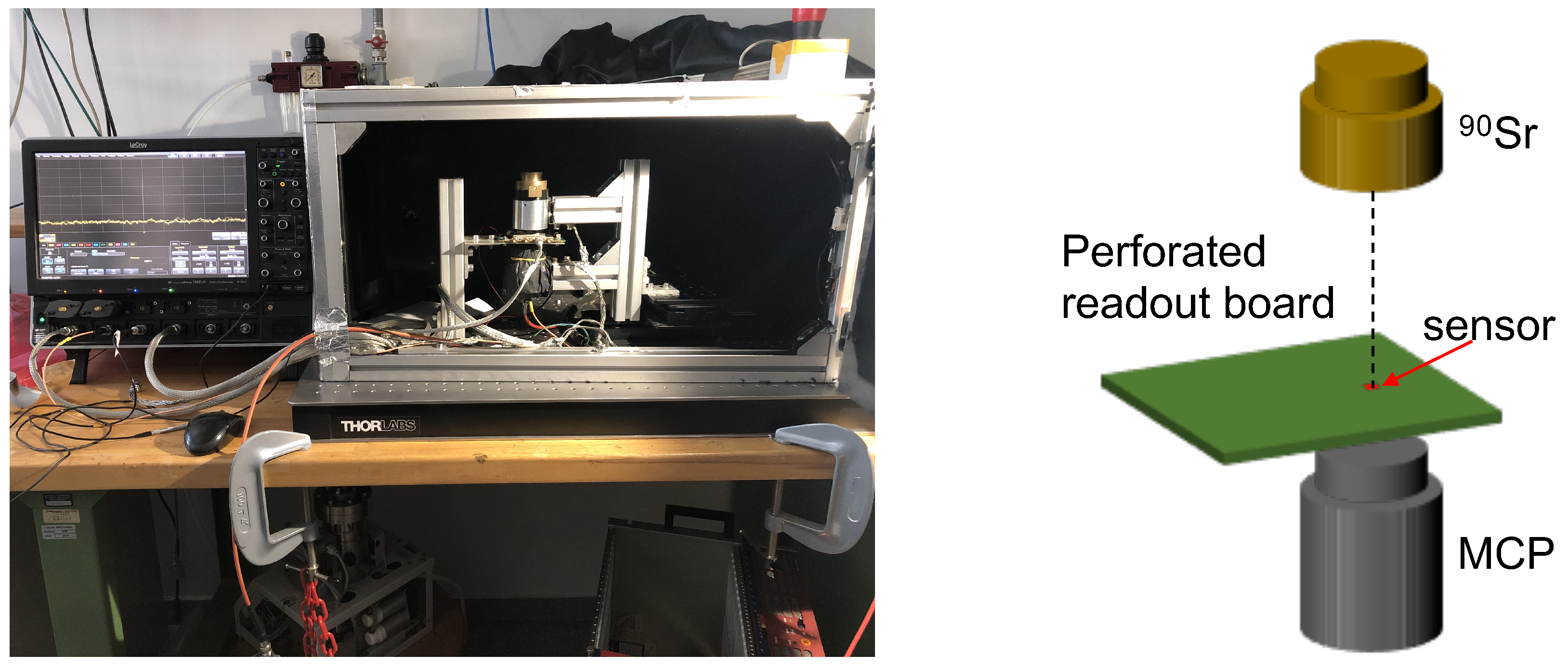
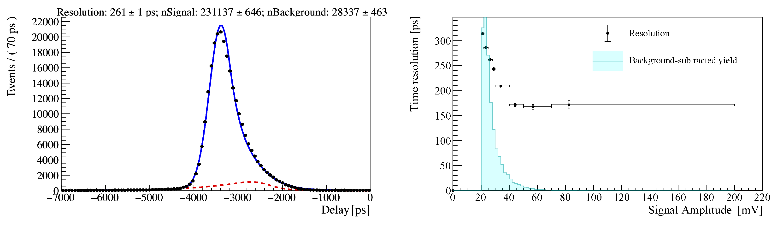
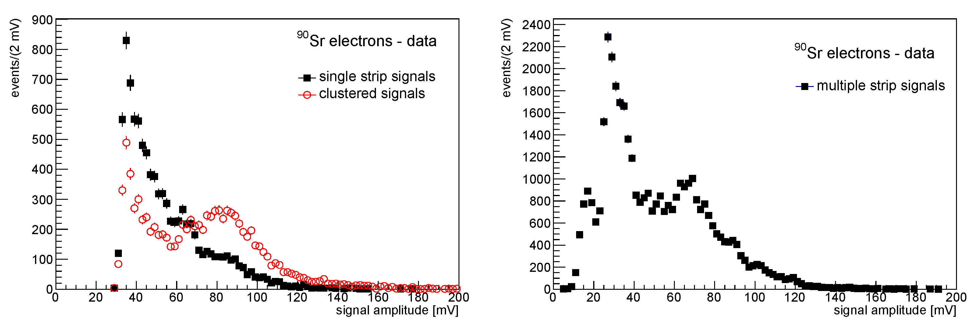
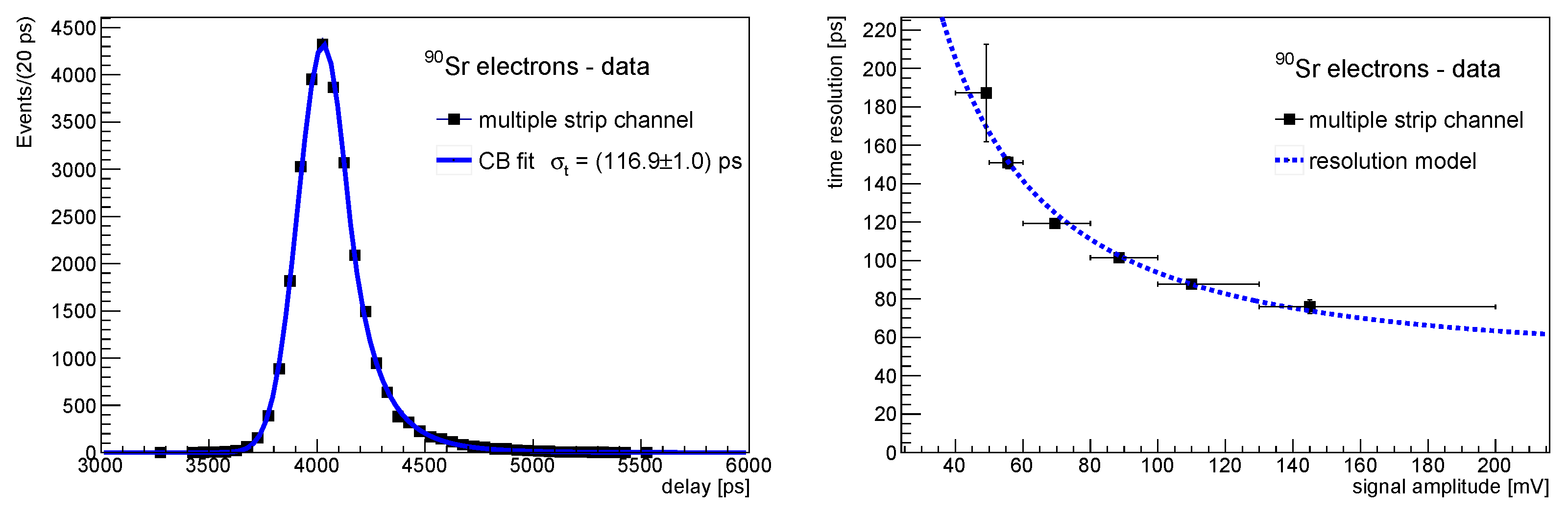
3.1. Test of First Prototype with Source
3.2. Test of First Prototype with High Energy Pions
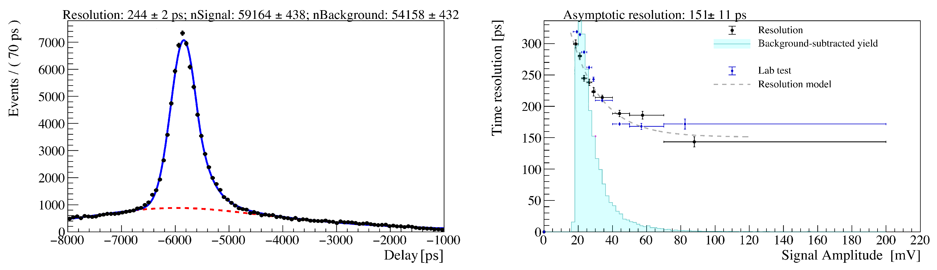
3.3. Preliminary Results on New Sensors with Source
4. Sensor Simulation Results
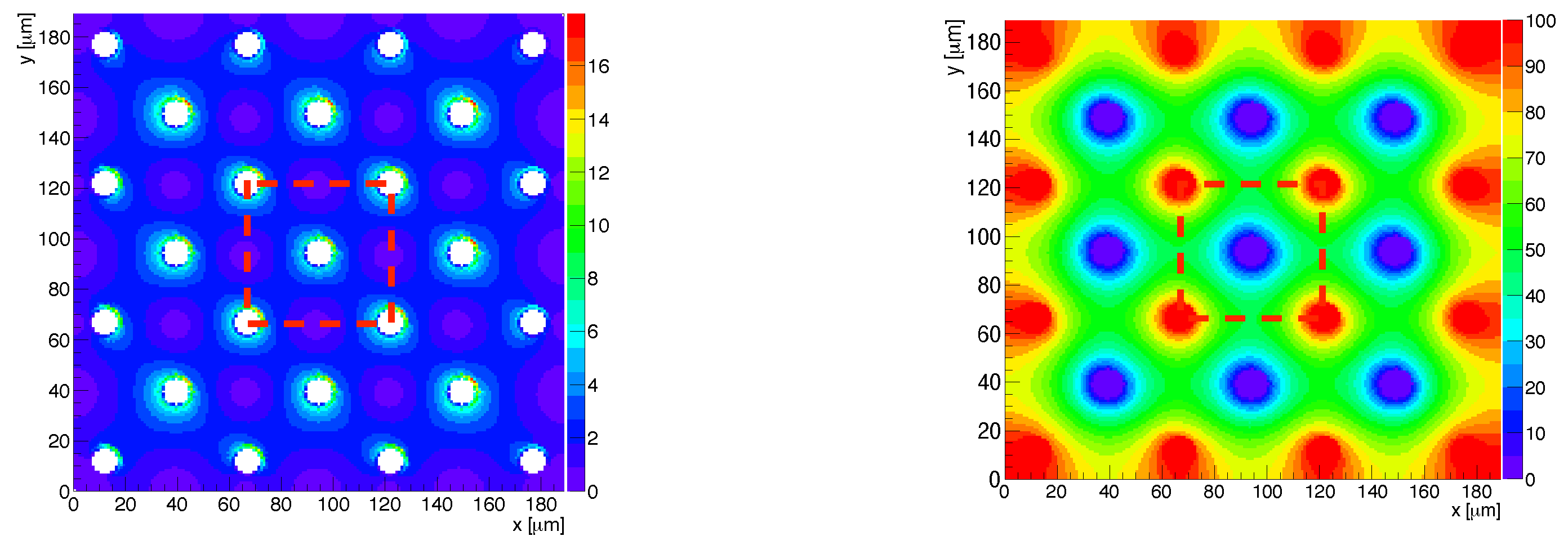
4.1. Simulation Flow
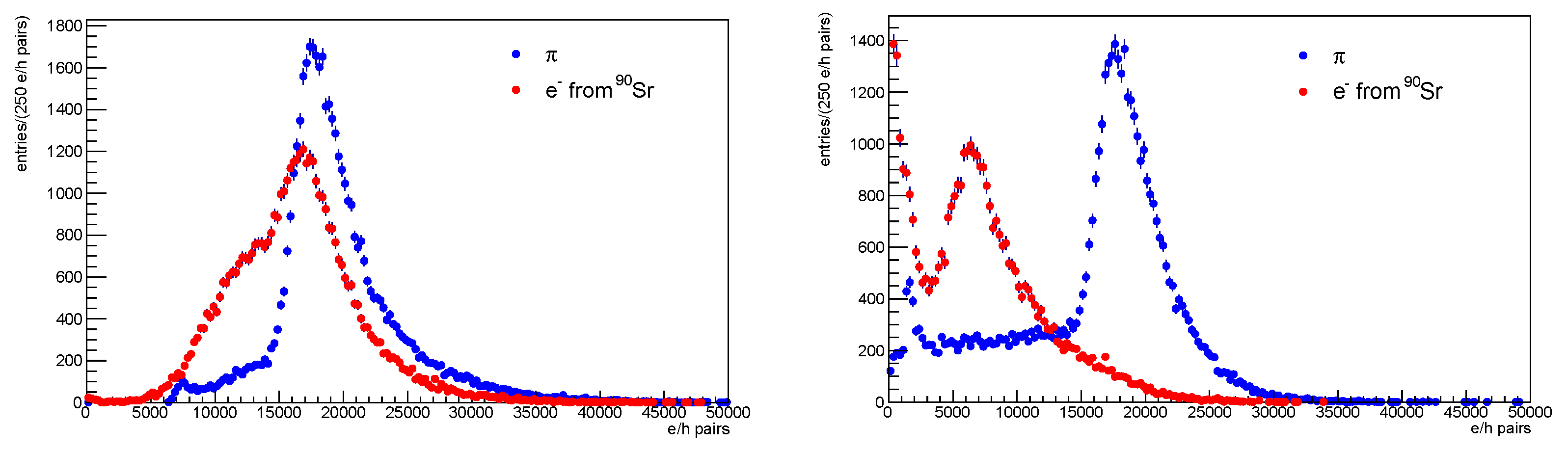
4.2. Simulation Results
5. Conclusions
Author Contributions
Funding
Institutional Review Board Statement
Informed Consent Statement
Data Availability Statement
Acknowledgments
Conflicts of Interest
References
- Abada, A.; Abbrescia, M.; AbdusSalam, S.S.; Abdyukhanov, I.; Abelleira Fernandez, J.; Abramov, A.; Aburaia, M.; Acar, A.O.; Adzic, P.R.; Agrawal, P.; et al. FCC-hh: The Hadron Collider. Eur. Phys. J. Spec. Top. 2019, 228, 755–1107. [Google Scholar] [CrossRef]
- Parker, S.; Kenney, C.; Segal, J. 3D—A proposed new architecture for solid-state radiation detectors. Nucl. Instrum. Methods Phys. Res. Sect. A Accel. Spectrometers Detect. Assoc. Equip. 1997, 395, 328–343. [Google Scholar] [CrossRef]
- Anderlini, L.; Aresti, M.; Bizzeti, A.; Boscardin, M.; Cardini, A.; Dalla Betta, G.F.; Ferrero, M.; Forcolin, G.; Garau, M.; Lai, A.; et al. Intrinsic time resolution of 3D-trench silicon pixels for charged particle detection. JINST 2020, 15, P09029. [Google Scholar] [CrossRef]
- Sadrozinski, H.F.W.; Seiden, A.; Cartiglia, N. 4D tracking with ultra-fast silicon detectors. Rep. Prog. Phys. 2017, 81, 026101. [Google Scholar] [CrossRef] [PubMed]
- Kononenko, T.; Komlenok, M.; Pashinin, V.; Pimenov, S.; Konov, V.; Neff, M.; Romano, V.; Läthy, W. Femtosecond laser microstructuring in the bulk of diamond. Diam. Relat. Mater. 2009, 18, 196–199. [Google Scholar] [CrossRef]
- Oh, A.; Caylar, B.; Pomorski, M.; Wengler, T. A novel detector with graphitic electrodes in CVD diamond. Diam. Relat. Mater. 2013, 38, 9–13. [Google Scholar] [CrossRef]
- Caylar, B.; Pomorski, M.; Bergonzo, P. Laser-processed three dimensional graphitic electrodes for diamond radiation detectors. Appl. Phys. Lett. 2013, 103, 043504. [Google Scholar] [CrossRef]
- Sun, B.; Salter, P.S.; Booth, M.J. High conductivity micro-wires in diamond following arbitrary paths. Appl. Phys. Lett. 2014, 105, 231105. [Google Scholar] [CrossRef]
- Lagomarsino, S.; Bellini, M.; Corsi, C.; Gorelli, F.; Parrini, G.; Santoro, M.; Sciortino, S. Three-dimensional diamond detectors: Charge collection efficiency of graphitic electrodes. Appl. Phys. Lett. 2013, 103, 233507. [Google Scholar] [CrossRef]
- Lagomarsino, S.; Bellini, M.; Corsi, C.; Cindro, V.; Kanxheri, K.; Morozzi, A.; Passeri, D.; Servoli, L.; Schmidt, C.J.; Sciortino, S. Radiation hardness of three-dimensional polycrystalline diamond detectors. Appl. Phys. Lett. 2015, 106, 193509. [Google Scholar] [CrossRef]
- Anderlini, L.; Bellini, M.; Bizzeti, A.; Cardini, A.; Ciaranfi, R.; Corsi, C.; Garau, M.; Lai, A.; Lagomarsino, S.; Lampis, A.; et al. Fabrication and Characterisation of 3D Diamond Pixel Detectors With Timing Capabilities. Front. Phys. 2020, 8, 589844. [Google Scholar] [CrossRef]
- Bossini, E.; Minafra, N. Diamond Detectors for Timing Measurements in High Energy Physics. Front. Phys. 2020, 8, 248. [Google Scholar] [CrossRef]
- Gracio, J.J.; Fan, Q.H.; Madaleno, J.C. Diamond growth by chemical vapour deposition. J. Phys. D Appl. Phys. 2010, 43, 374017. [Google Scholar] [CrossRef]
- Schwander, M.; Partes, K. A review of diamond synthesis by CVD processes. Diam. Relat. Mater. 2011, 20, 1287–1301. [Google Scholar] [CrossRef]
- Salter, P.S.; Baum, M.; Alexeev, I.; Schmidt, M.; Booth, M.J. Exploring the depth range for three-dimensional laser machining with aberration correction. Opt. Express 2014, 22, 17644–17656. [Google Scholar] [CrossRef] [PubMed]
- Salter, P.S.; Booth, M.J.; Courvoisier, A.; Moran, D.A.J.; MacLaren, D.A. High resolution structural characterisation of laser-induced defect clusters inside diamond. Appl. Phys. Lett. 2017, 111, 081103. [Google Scholar] [CrossRef]
- Ashikkalieva, K.; Kononenko, T.; Obraztsova, E.; Zavedeev, E.; Khomich, A.; Ashkinazi, E.; Konov, V. Direct observation of graphenic nanostructures inside femtosecond-laser modified diamond. Carbon 2016, 102, 383–389. [Google Scholar] [CrossRef]
- Piccolo, L.; Rivetti, A.; Cadeddu, S.; Casu, L.; Lai, A.; Barbaro, M.; Napoli, C.; Sonedda, S.; Frontini, L.; Liberali, V.; et al. The first ASIC prototype of a 28 nm time-space front-end electronics for real-time tracking. PoS 2020, TWEPP2019, 022. [Google Scholar] [CrossRef][Green Version]
- Minafra, N.; Al Ghoul, H.; Arcidiacono, R.; Cartiglia, N.; Forthomme, L.; Mulargia, R.; Obertino, M.; Royon, C. Test of Ultra Fast Silicon Detectors for picosecond time measurements with a new multipurpose read-out board. Nucl. Instrum. Methods Phys. Res. Sect. A Accel. Spectrometers Detect. Assoc. Equip. 2017, 867, 88–92. [Google Scholar] [CrossRef][Green Version]
- Pivk, M.; Le Diberder, F. sPlot: A statistical tool to unfold data distributions. Nucl. Instrum. Methods Phys. Res. Sect. A Accel. Spectrometers Detect. Assoc. Equip. 2005, 555, 356–369. [Google Scholar] [CrossRef]
- Skwarnicki, T. A Study of the Radiative Cascade Transitions between the Upsilon-Prime and Upsilon Resonances. Ph.D. Thesis, Institute of Nuclear Physics, Krakow, Poland, 1986. [Google Scholar]
- Morozzi, A.; Passeri, D.; Kanxheri, K.; Servoli, L.; Lagomarsino, S.; Sciortino, S. Polycrystalline CVD diamond device level modeling for particle detection applications. J. Instrum. 2016, 11, C12043. [Google Scholar] [CrossRef]
- Morozzi, A.; Sciortino, S.; Anderlini, L.; Servoli, L.; Kanxheri, K.; Lagomarsino, S.; Passeri, D. 3D Diamond Tracking Detectors: Numerical analysis for Timing applications with TCAD tools. J. Instrum. 2020, 15, C01048. [Google Scholar] [CrossRef]
- Brun, R.; Rademakers, F. ROOT: An object oriented data analysis framework. Nucl. Instrum. Meth. A 1997, 389, 81–86. [Google Scholar] [CrossRef]
- Kramberger, G. KDetSim—A Simple Way to Simulate Detectors. 2016. Available online: https://github.com/IJSF9Software/KDetSim (accessed on 12 December 2021).
- Agostinelli, S.; Allison, J.; Amako, K.A.; Apostolakis, J.; Araujo, H.; Arce, P.; Asai, M.; Axen, D.; Banerjee, S.; Barr, G.J.N.I.; et al. Geant4: A simulation toolkit. Nucl. Instrum. Meth. 2003, A506, 250. [Google Scholar] [CrossRef]
- Allison, J.; Amako, K.; Apostolakis, J.; Araujo, H.; Dubois, P.; Asai, M.; Barrand, G.; Capra, R.; Chauvie, S.; Chytracek, R.; et al. Geant4 developments and applications. IEEE Trans. Nucl. Sci. 2006, 53, 270. [Google Scholar] [CrossRef]
- Riegler, W.; Windischhofer, P. Signals induced on electrodes by moving charges, a general theorem for Maxwell’s equations based on Lorentz-reciprocity. Nucl. Instr. Meth. A 2020, 980, 164471. [Google Scholar] [CrossRef]


Publisher’s Note: MDPI stays neutral with regard to jurisdictional claims in published maps and institutional affiliations. |
© 2021 by the authors. Licensee MDPI, Basel, Switzerland. This article is an open access article distributed under the terms and conditions of the Creative Commons Attribution (CC BY) license (https://creativecommons.org/licenses/by/4.0/).
Share and Cite
Anderlini, L.; Bellini, M.; Corsi, C.; Lagomarsino, S.; Lucarelli, C.; Passaleva, G.; Sciortino, S.; Veltri, M. Fabrication and First Full Characterisation of Timing Properties of 3D Diamond Detectors. Instruments 2021, 5, 39. https://doi.org/10.3390/instruments5040039
Anderlini L, Bellini M, Corsi C, Lagomarsino S, Lucarelli C, Passaleva G, Sciortino S, Veltri M. Fabrication and First Full Characterisation of Timing Properties of 3D Diamond Detectors. Instruments. 2021; 5(4):39. https://doi.org/10.3390/instruments5040039
Chicago/Turabian StyleAnderlini, Lucio, Marco Bellini, Chiara Corsi, Stefano Lagomarsino, Chiara Lucarelli, Giovanni Passaleva, Silvio Sciortino, and Michele Veltri. 2021. "Fabrication and First Full Characterisation of Timing Properties of 3D Diamond Detectors" Instruments 5, no. 4: 39. https://doi.org/10.3390/instruments5040039
APA StyleAnderlini, L., Bellini, M., Corsi, C., Lagomarsino, S., Lucarelli, C., Passaleva, G., Sciortino, S., & Veltri, M. (2021). Fabrication and First Full Characterisation of Timing Properties of 3D Diamond Detectors. Instruments, 5(4), 39. https://doi.org/10.3390/instruments5040039