Article

Transformer Coupling and Its Modelling for the Flux-Ramp Modulation of rf-SQUIDs

1
Dipartimento di Fisica G. Occhialini, Università degli Studi di Milano Bicocca, Piazza della Scienza 3, 20126 Milano, Italy
2
INFN sez. di Milano Bicocca, Piazza della Scienza 3, 20126 Milano, Italy
*
Author to whom correspondence should be addressed.
Instruments 2019, 3(1), 3; https://doi.org/10.3390/instruments3010003
Submission received: 5 November 2018 / Revised: 13 December 2018 / Accepted: 24 December 2018 / Published: 29 December 2018

Abstract

:
Microwave SQUID (Superconducting QUantum Interference Device) multiplexing is a suitable technique for reading a large number of detector channels, using only a few connecting lines. In the HOLMESexperiment, this is based on inductively coupled rf-SQUIDs fed by TES (Transition Edge Sensors). Operation of the whole rf-SQUID chain is achieved with a single transmission line, by means of the recently introduced flux-ramp modulation technique—a sawtooth signal which allows signal reconstruction while operating the rf-SQUIDs in an open loop condition. Due to the crucial role of the sawtooth signal, it is very important that it does not suffer from ground-loop disturbances and electromagnetic interference (EMI). Introducing a transformer between the sawtooth source and the SQUID is very effective in suppressing disturbances. The sawtooth signal has both slow and fast components, and the frequency can vary between a few kHz up to a MHz, depending on the TES signal and SQUID characteristics. A transformer able to handle such a broad range of conditions must have very stringent characteristics and needs to be custom designed. Our solution exploits standard commercial and inexpensive transformers for LAN networks, stacked in a user-selectable number, to better fit the bandwidth requirements. A model that allows handling of the low- and high-frequency operating range has been developed.

1. Introduction

The use of SQUIDs (Superconducting QUantum Interference Devices) in cryogenic particle detectors allows implementation of the readout of large arrays using different configurations. A promising approach for reading out a large number of detectors with a SQUID array using a common transmission line is microwave rf-SQUID multiplexing. This technique can be leveraged to read the signals from many detectors with high energy resolution and a large signal bandwidth. A multiplexed microwave readout will be used in the HOLMES detectors [1], an array of 1000 micro-calorimeters based on TES (Transition Edge Sensors) [2], each coupled to a rf-SQUID. The HOLMES detectors are Mo/Cu bilayer TESs with gold absorbers, in which 163 Ho ions will be implanted [3]. HOLMES aims to push the sensitivity on the neutrino mass below 1 eV, by performing a calorimetric measurement of the energy released in the electron capture decay of 163 Ho.
The rf-SQUID is a superconducting ring interrupted by a thin insulating layer, the Josephson tunnel junction, through which Josephson tunnelling is possible. In a very simplified picture, by coupling the SQUID to a magnetic field, the flux through the ring is quantized and the resulting current in the loop is [4,5,6,7]:
i = I 0 sin 2 π Φ t o t Φ 0 , Φ 0 = h 2 e ,
where I 0 is a current dependent on SQUID composition, Φ t o t is the total induced flux, and Φ 0 is the flux quantum. Figure 1 shows a typical single channel rf-SQUID readout. The rf-SQUID is the circle with a cross, which represents the Josephson tunnel junction. The rf-SQUID is inductively coupled to the TES, with the RF bias Φ b i a s , and the feedback that sets the working point (see the plot at the bottom of the figure). The feedback forces the flux Φ f e e d in the rf-SQUID opposite to the input flux Φ s i g in order to maintain the total flux constant, generating an unbalance in the amplifier output voltage proportional to Φ s i g (The scheme of Figure 1 is over-simplified, since the RF bias is removed from the signal by means of an additional circuit block at the amplifier output, not shown). The flux generated from the signal is much slower than that of the RF bias, and is easily de-convolved at the amplifier output.
The classical set-up of Figure 1 is not convenient when one wants to minimize the number of connecting lines to the array, since every channel needs its own feedback link. To overcome this limitation, flux-ramp modulation was recently successfully implemented. A simplified scheme is displayed in Figure 2. We give here a very short description of its principles of operation. Details can be found in [8,9,10], where this technique was introduced for the first time. Now, the rf-SQUID is operated open-loop and it is fed by the sawtooth signal generator (ST). Provided that the period of the sawtooth is an integer multiple of the ratio of the flux quanta over its flux slope, d Φ / d t , the rf-SQUID current, as depicted at the bottom of the figure, is then given by:
i = I 0 sin 2 π S r t Φ 0 + 2 π Φ s i g Φ 0 , S r = d Φ d t .
If the frequency of the sawtooth is much higher than the highest frequency component of the input signal, then the signal can be considered as a pure phase term. By evaluating the phase shift as a function of time, the signals due to particle interactions are properly reconstructed. This is depicted in Figure 2, where feedback is not needed anymore, and the ST signal can be common to all of the rf-SQUIDs in the array. Now that we are able to feed all the rf-SQUIDs with a single line, we need to do the same with the reading of the rf-SQUID outputs. To tag every channel, a stub of different length is connected in series to every rf-SQUID output inductor, in such a way that every stub resonates at the frequency for which the stub is a quarter wavelength: The S u m _ o f _ s i n e s generator will therefore provide a superimposition of sinusoidal tones applied to this common line, read out by a cryogenic High Mobility Transistor (HEMT) amplifier. In this way, the signal from every rf-SQUID will modulate its own tone. So far, only two transmission lines are needed to operate the rf-SQUID array: One to read out the output signals, and the other to provide the ramp signal.
As stated above, the sawtooth frequency must be larger than the highest frequency components of the input signal. At the same time, it is limited by the sampling frequency of the ADC. For the final configuration of HOLMES, the detector signal-rise time is expected to be close to 10 μ s, and the ramp frequency will be set to 500 kHz. In the current R&D studies, however, it is required to work down to small frequencies, as several TES optimized for different ranges are foreseen. Since the flux-ramp modulation has a crucial role in the reconstruction of the signal, any disturbance, such as ground-loop and EMI, must be suppressed. In this paper, we describe our solution based on the use of a coupling transformer between the signal generator ST and the rf-SQUID coil of Figure 2. Two main requirements need to be satisfied: The rise of the sawtooth must be a straight line so that the oscillation pattern of the rf-SQUID is preserved over time, and the fall time of the sawtooth must be fast enough to guarantee phase alignment. This is obtained if the transformer presents a flat frequency response from the sawtooth fundamental, up to a frequency about ten times larger. Since the frequency of the sawtooth is expected to be in the range from a few kHz to 500 kHz, the transformer should provide a flat response between a few kHz to a few MHz. We developed a simple circuit, based on the use of commercial and inexpensive transformers for LAN networks, avoiding the design and construction of an ad hoc device. The circuit allows selection of a suitable number of transformers to be connected in series, in order to increase their low-frequency input impedance, matching, and to preserve the sawtooth shape. In addition, the selection of value of an impedance, to be connected in parallel to the input coil of the transformer, gives additional flexibility. To confirm the validity of the developed system, we characterize and model the transformers.

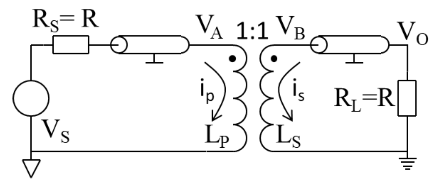
2. Principles of Operation and Modeling

The ideal principle of operation is in Figure 3: The source of the signal drives the primary coil of the transformer through a coaxial line, terminated at its input with R S . The secondary coil of the transformer drives the load impedance R L at the end of the coaxial line. The primary and secondary coils are equal, and the ratio of the input to the output coil voltage is one. To preserve the shape of the fast component of the sawtooth signal, reflection across the transmission lines must be avoided, and the terminating resistors R S and R L must be equal to the characteristic line impedance (50 Ω in our case). In this arrangement, the input and output grounds are isolated and ground-loops and EMI disturbances are strongly suppressed.
The dropout voltage V A across the input coil equals the sum of the voltage across the input inductance, L p , and the voltage due to the mutual inductance, M. A similar consideration applies to V B and the output coil, L s . In the complex frequency domain ( s = i ω ) the network is ruled by
V A = s M i s + s L p i p ,
V B = s M i p + s L s i s .
The system of equations that solve the network of Figure 3 is then
V s V A R = V A s M i s s L p s M i p + s L s i s + R i s = 0 .
If we consider M = L p L s and L p L s , the solution is
V o = i s R = s L p 2 s L p + R V s .
From (6), the absolute value of the transfer function is zero at DC, increases up to the cutoff frequency, and is flat from the cutoff frequency upwards. This ideal model does not fully describe the real behavior of the circuit, and we identified two major effects that led us to formulate a more accurate model, described below.
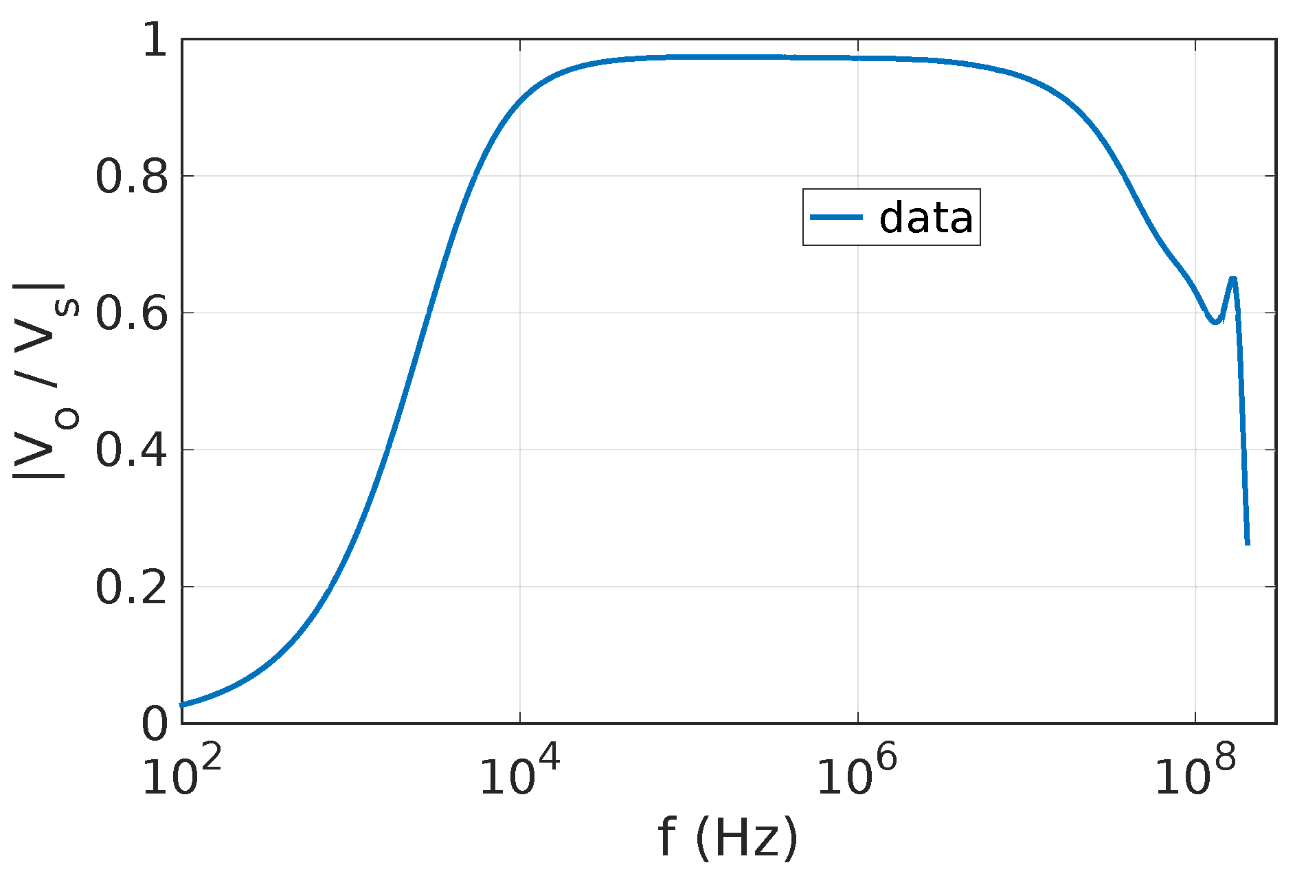
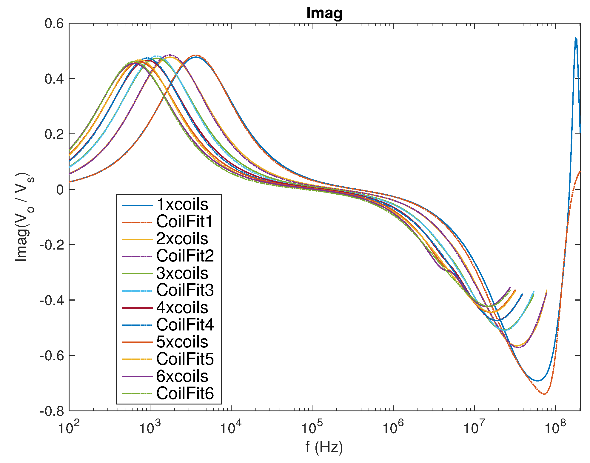
  • The first deviation from the ideal model can be appreciated from the measured transfer function obtained with the selected transformer (Würth Elektronik 749012011), shown in Figure 4: A high-frequency roll-off, not predicted by (6), is present. We have verified that this high-frequency limitation deteriorates if the value of the load impedance R L is decreased. This can be modeled with the presence of a small parasitic inductance L P A R in series to the output of the transformer, forming a low pass filter with termination resistance R L .
  • The roll-off gets a 20 dB/dec slope, due to the pole R L / L P A R , only at high frequency, but shows a smaller slope near its 3 db frequency. This second effect can be accounted for by the presence of some distributed parasitic capacitance between and within the coils.
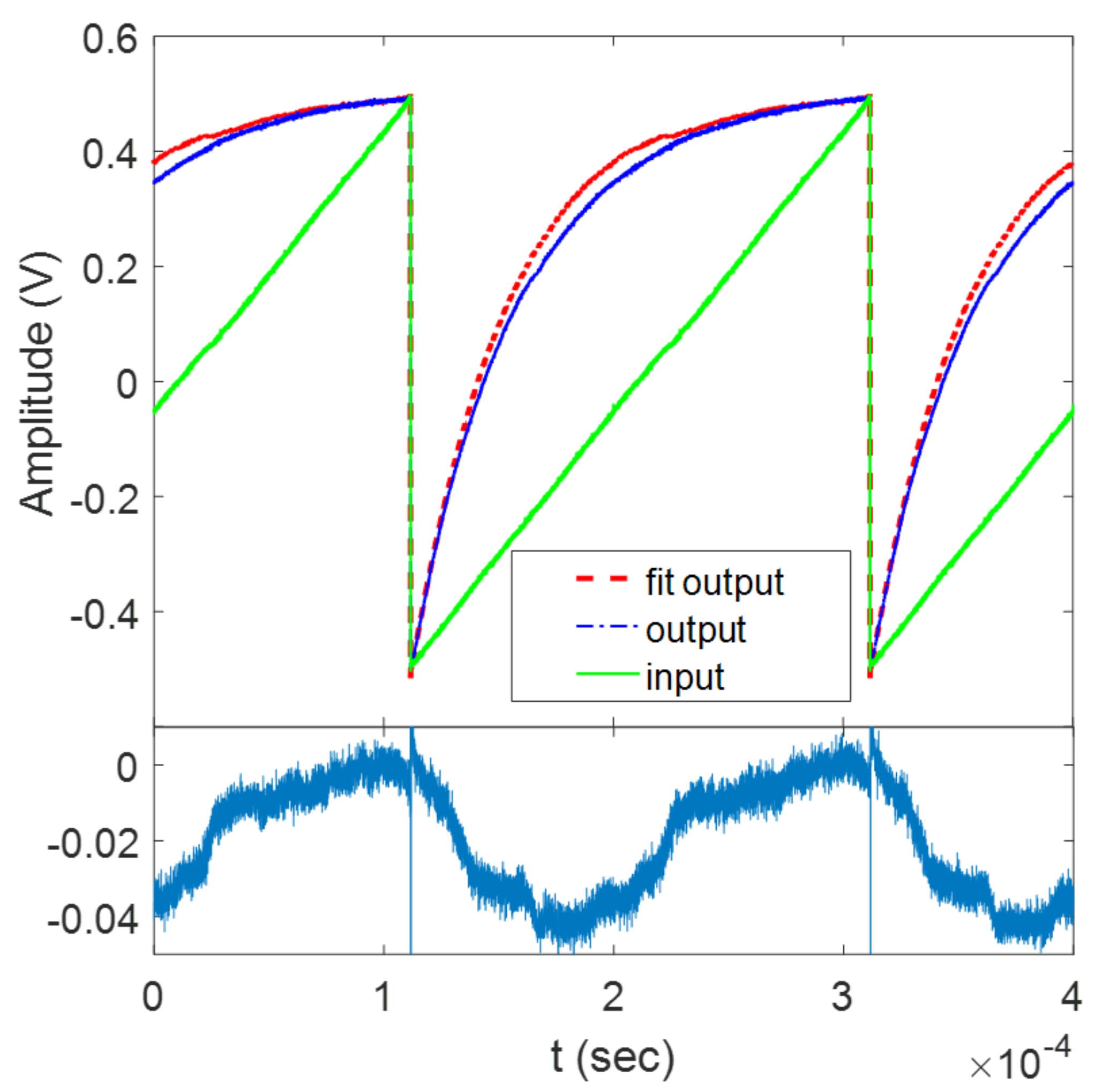
To pursue our final aim of implementing a system capable of replicating undistorted sawtooth signals, we developed an essential model which summarizes several previous circuit solutions [11,12,13,14,15,16,17,18,19], all based on passive networks. We know from circuit theory that the transfer function of a passive network in the frequency domain is the ratio of two polynomials. The degree of the denominator, having roots with negative real part, is greater than or equal to that of the numerator, which can have negative or positive roots to shape the phase properly. So, rather than trying to find a passive network that gives the desired response, we left it implicit and we described its behavior with the ratio of two same-degree polynomials, a ( ω ) , as the final frequency roll-off is left accounted for by the pole at R L / L P A R . The term a ( ω ) is used to bind the input and output windings of the transformer:
L s = a ( ω ) 2 L p = ( 1 + s z A ) ( 1 + s z B ) ( 1 + s p A ) ( 1 + s p B ) 2 L p .
The squaring of a ( ω ) is convenient as the final transfer function is linearly dependent on a ( ω ) , while the two poles and zeros are the minimum number of parameters we found adequate to fit the data. The final model is shown in Figure 5 with the transformer inside the dashed rectangle. The transformer is seen as an ideal transformer (namely, a voltage generator) having as input impedance the primary coil L P in parallel to Z L = ( K a ( ω ) ) 2 ( s L P A R + R L ) s L P A R + R L . The coefficient K 1 accounts for tolerance in the component values, and R, R S E R , and R L are additional components mounted on the board. The network now has independent input and output loops, and is easily solved:
V A = s L p R I N ( R L + s L P A R ) s L p | | R I N | | ( R L + s L P A R ) + R + R S E R V S V o = K a ( ω ) R L s L P A R + R L V A .
In order to obtain the ratio V o / V s , we used the MATLAB Symbolic Math toolbox and its least-squares solver. Figure 6 shows the imaginary and real components of the transfer functions of the selected transformer (Würth Elektronik 749012011) fitted with the new model. The model fits the measured data fairly well, except for a small deviation at high frequency.
Now, we have to analyse the behaviour of the transformer response to a sawtooth input signal. Figure 7 shows this for a 5 kHz frequency, which highlights the limitation: The linear rising part is largely bent. The reason for this is understood, looking at the first relation of (8): V A is AC-coupled to V S , with a zero at the origin. The proportionality becomes flat only above the frequencies at which s L P approaches R L R I N . To lower this frequency, we can follow two methods:
  • Lower the value of R L R I N : In this case, the signal V A will be attenuated and V S will need to be increased to maintain the appropriate output value (there is a lower limit in frequency beyond which the transformer core saturates); and/or
  • Increase the value of the inductance L p of the primary coil.
The latter approach is often pursued by designing an ad hoc transformer with an optimal number of turns. With a large number of turns, the impact of parasitic capacitance and a possible increase in L P A R should be considered. Since we need to face a broad range of sawtooth signals, from a few kHz up to a MHz, we chose to implement a set-up that we call a trimmable-transformer, consisting of several transformers (as the one characterized) connected in series, in order to match the low/high frequency needs. In the final set-up, both approaches described above can then be followed, depending on the signal characteristics.

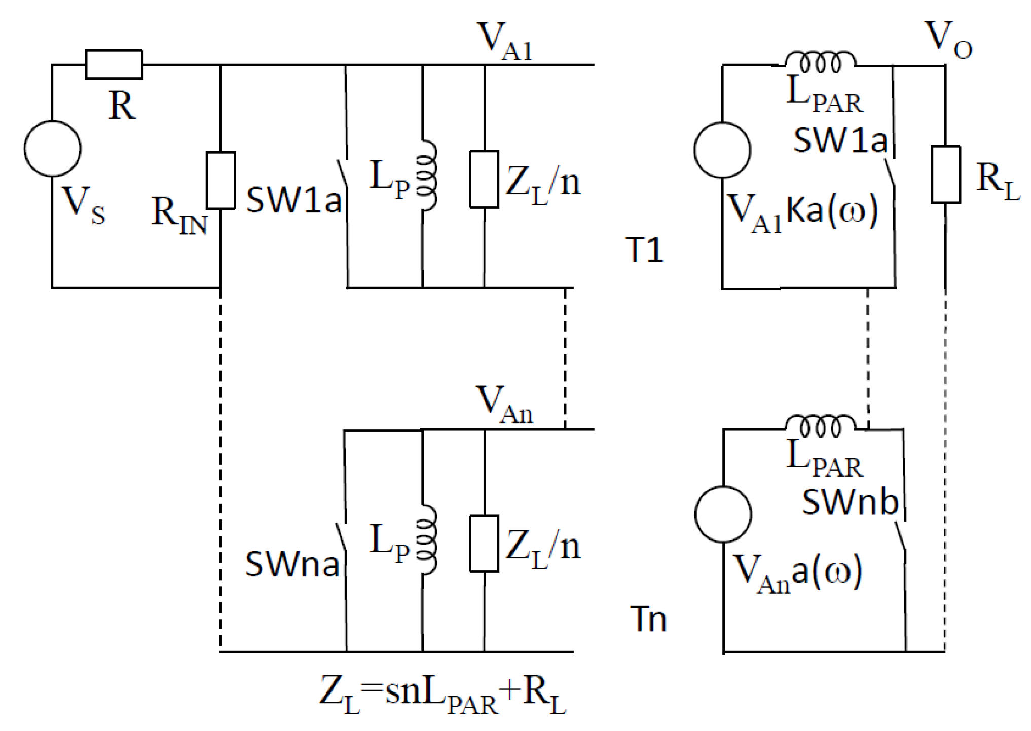
3. The Trimmable-Transformer Set-Up and Results

3.1. Circuit Description

The circuit arrangement of our trimmable-transformer is shown in Figure 8. All transformers and resistors show a tolerance with respect to the nominal values, but we are interested in the overall output, so we summarize all non-idealities in only one global parameter K.
A number n of transformers can be connected in series, thanks to the presence of a set of switch pairs S W x a and S W x b with 1 x n , which enable (open position) or disable (short position) the corresponding transformer. Each transformer is modeled with the circuit of Figure 5. When the switches are all in open state, the primary has, at its input, the load impedance Z L divided by n. If γ is the number of switches left open, then the equivalent circuit looks as in Figure 9 and:
V A = s γ L p R I N ( R L + s γ L P A R ) s γ L p R I N ( R L + s γ L P A R ) + R + R S E R V S V o = K a ( ω ) R L s γ L P A R + R L V A .
As evidenced by the first equation of (9), the primary coil has an impedance γ times larger and, since R I N and R L remain the same, the low frequency coupling is shifted to a lower frequency. At the same time, from the second equation of (9), the parasitic impedance at the secondary coil is increased to s γ L P A R and the high frequency roll-off is lowered, too. By increasing the number of transformers, both the low frequency coupling and the high frequency roll-off are lowered. A trade-off can be found: The lower the sawtooth frequency, the less is required from the speed of its fast transition, and vice versa for a high frequency sawtooth. The Würth Elektronik 749012011 has a pair of transformers. We used 3 of these devices for a total of 6 coupled transformers, each one with a pair of configurable switches. Figure 10 depicts our layout.

3.2. Measurement Results

Measurements were taken in both time and frequency domains. We first characterized the transfer functions with an Agilent 4395A spectrum/network analyzer and extracted the parameters of our model (8) with the various available configurations of Figure 8. Results and simulated transfer functions of the series of one to six transformers are shown in Figure 11 and Figure 12 for the real and imaginary parts. Inductance L P was about 1090 μ H, which grows linearly, up to about 6200 μ H when 6 transformers were put in series. The parasitic inductor L P A R was also found to be linearly dependent on the number of transformers, with a value that was close to 500 nH for one transformer, up to 1700 nH for six transformers. A pedestal of about 200 nH resulted in this latter case, probably due to the board layout. The sensitivity to z A , z B , p A and p B lowered with the number of transformers, due to the decreasing value of the cut-off frequency R L / L P . With one transformer it resulted in −72 MHz and 138 MHz, for z A and z B , respectively; and around −150 MHz for p A and p B . A summary of the fit parameters is in Table 1.
Time domain studies were done, applying the sawtooth signals and downloading the responses from an oscilloscope. The simulated behaviors were determined from the parameters, measured with the network analyzer. Figure 13 shows the response, superimposed to a 5 kHz sawtooth input signal when six transformers are connected in series, R I N = 4.7 Ω and R S E R = 47 Ω . R S E R is at the receiving end of the coaxial cable. It is used to set the input impedance of the circuit, given by the sum of R S E R itself and the impedance at the transformer input, at 50 Ω . We can see now that the response matches the input, compared to the response of Figure 7. The response to a faster sawtooth at 1 MHz frequency is shown in Figure 14, where only one transformer is used with R I N = and R S E R = 0 . In this way, the fast transition is satisfied, as well. Another example is reported in Figure 15 where the signal is 10 kHz, R I N = 11 Ω ( R S E R = 39 Ω ) and γ = 4: The output signal is almost indistinguishable from the input signal. The accuracy of the injected signal and scope data is at about 1% level, and this limits our evaluation of the residuals. Simulated curves are very close to the superimposed measured signals in Figure 13, Figure 14 and Figure 15, proving the validity of our model. In Figure 16, we emulated the sinusoidal shape of the quantized current in (2) at 25 kHz when the sawtooth is at 5 kHz, for the case R I N = 4.7 Ω and R S E R = 47 Ω . This sawtooth frequency is the lowest that ensures a good transmission with a negligible error, with respect to the sinusoid generated from the input signal.

4. Conclusions

The necessity to provide a sawtooth signal to multiplexed rf-SQUIDs which does not suffer from ground-loop disturbances and EMI has triggered the development and modeling of the trimmable-transformer; a circuit set-up which enables implementation of a 1:1 transformer ratio with different values in the primary and secondary coil inductances. This trimmable-transformer is composed of commercial SMD standard transformers, and can be configured to match the required AC-coupling frequency with adequate bandwidth. Changing the number of transformers from one to six and/or the input resistance results in a pass-band shift by a factor ≈14. This allows the coverage of sawtooth signals over the frequency range of our application, from 5 kHz up to 1 MHz.

Author Contributions

Conceptualization, E.F. and G.P.; investigation, P.C., L.C., M.F., E.F., A.G., C.G., M.M, A.N., G.P. and A.P.; resources, A.N. and G.P.; writing—original draft preparation, E.F. and G.P.; writing—review and editing, E.F, C.G. and G.P.; supervision, A.N. and G.P.; project administration, A.N.; funding acquisition, A.N.

Funding

This research was funded by European Research Council (FP7/2007-2013) grant HOLMES, number 340321.

Conflicts of Interest

The authors declare no conflict of interest.

References

  1. Alpert, B.; Balata, M.; Bennett, D.; Biasotti, M.; Boragno, C.; Brofferio, C.; Ceriale, V.; Corsini, D.; Day, P.K.; de Gerone, M.; et al. HOLMES. EPJ C 2015, 75, 112. [Google Scholar] [CrossRef] [PubMed] [Green Version]
  2. Hays-Wehle, J.P.; Schmidt, D.R.; Ullom, J.N.; Swetz, D.S. Thermal Conductance Engineering for High-Speed TES Microcalorimeters. J. Low Temp. Phys. 2016, 184, 492. [Google Scholar] [CrossRef]
  3. Orlando, A.; Ceriale, V.; Ceruti, G.; de Gerone, M.; Faverzani, M.; Ferri, E.; Gallucci, G.; Giachero, A.; Nucciotti, A.; Puiu, D.; et al. Microfabrication of Transition-Edge Sensor Arrays of Microcalorimeters with 163 Ho for Direct Neutrino Mass Measurements with HOLMES. J. Low Temp. Phys. 2018, 193, 771–776. [Google Scholar] [CrossRef]
  4. Barone, A.; Paternò, G. Physics and Applications of the Josephson Effect; John Wiley & Sons Inc.: Hoboken, NJ, USA, 1982. [Google Scholar]
  5. Clarke, J.; Braginski, A.I. The SQUID Handbook, Vol. I Fundamentals and Technology of SQUIDs and SQUID Systems; WILEY-VCH Verlag GmbH & Co. KGaA: Weinheim, Germany, 2004. [Google Scholar]
  6. Fagaly, R.L. Superconducting quantum interference device instruments and applications. Rev. Sci. Instrum. 2006, 77, 101101. [Google Scholar] [CrossRef]
  7. Giffard, R.P.; Webb, R.A.; Wheatley, J.C. Principles and Methods of Low-Frequency Electric and Magnetic Measurements Using an rf-Biased Point-Contact Superconducting Device. J. Low Temp. Phys. 1972, 6, 533–610. [Google Scholar] [CrossRef]
  8. Mates, J.A.B.; Irwin, K.D.; Vale, L.R.; Hilton, G.C.; Gao, J.; Lehnert, K.W. Flux-Ramp Modulation for SQUID Multiplexing. J. Low Temp. Phys. 2012, 167, 707. [Google Scholar] [CrossRef]
  9. Noroozian, O.; Mates, J.A.B.; Bennett, D.A.; Brevik, J.A.; Fowler, J.W.; Gao, J.; Hilton, G.C.; Horansky, R.D.; Irwin, K.D.; Kang, Z.; et al. Hig-resolution gamma-ray spectroscopy with a microwave-multiplexed transition-edge sensor array. Appl. Phys. Lett. 2013, 103, 202602. [Google Scholar] [CrossRef]
  10. Mates, J.A.B.; Hilton, G.C.; Irwin, K.D.; Lehnert, K.W.; Vale, L.R. Demonstration of a multiplexer of dissipationless superconducting quantum interference devices. Appl. Phys. Lett. 2008, 92, 023514. [Google Scholar] [CrossRef]
  11. Martinez, J.A.; Mork, B.A. Transformer Modeling for Low- and Mid-Frequency Transients—A Review. IEEE Trans. Power Deliv. 2005, 20, 1625–1632. [Google Scholar] [CrossRef]
  12. Lu, H.Y.; Zhu, J.G.; Hui, S.Y.R. Experimental Determination of Stray Capacitances in High Frequency Transformers. IEEE Trans. Power Electron. 2003, 18, 1105–1112. [Google Scholar]
  13. Abeywickrama, N.; Serdyuk, Y.V.; Gubanski, S.M. High-Frequency Modeling of Power Transformers for Use in Frequency Response Analysis (FRA). IEEE Trans. Power Deliv. 2008, 23, 2042–2049. [Google Scholar] [CrossRef]
  14. Zhang, Z.; Lu, F.; Liang, G. A High-Frequency Circuit Model of a Potential Transformer for the Very Fast Transient Simulation in GIS. IEEE Trans. Power Deliv. 2008, 23, 1995–1999. [Google Scholar]
  15. Morched, A.; Mad, L.; Ottevangers, J. A High Frequency Transformer Model for the EMTP. IEEE Trans. Power Deliv. 1993, 8, 1615–1626. [Google Scholar] [CrossRef]
  16. Tziouvaras, D.A.; McLaren, P.; Alexander, G.; Dawson, D.; Esztergalyos, J.; Fromen, C.; Glinkowski, M.; Hasenwinkle, I.; Kezunovic, M.; Kojovic, L.; et al. Mathematical Models for Current, Voltage, and Coupling Capacitor Voltage Transformers. IEEE Trans. Power Deliv. 2000, 15, 62–71. [Google Scholar] [CrossRef]
  17. Vaessen, P.T.M.; Kema, N.V. Transformer Model For High Frequencies. IEEE Trans. Power Deliv. 1998, 3, 1761–1768. [Google Scholar] [CrossRef]
  18. Islam, S.M.; Coates, K.M.; Ledwich, G. Identification of High Frequency Transformer Equivalent Circuit Using Matlab from Frequency Domain Data. In Proceedings of the IEEE Industry Applications Society Annual Meeting, New Orleans, LA, USA, 5–9 October 1997; pp. 357–364. [Google Scholar]
  19. Dessaint, L.A.; Al-Haddad, K.; Le-Huy, H.; Sybille, G.; Brunelle, P. A Power System Simulation Tool Based on Simulink. IEEE Trans. Ind. Electron. 1999, 46, 1252–1254. [Google Scholar] [CrossRef]
Figure 1. Simplified diagram of a rf-SQUID linked to a TES sensor and read out in closed-loop configuration. The rf-SQUID is the circle with a cross that represents the Josephson tunnelling junction, coupled to 3 inductors: The rf-bias and reading node, the feedback, and the signal inductors. The diagram represents (1). Φ f e e d = Φ s i g , and the output voltage is proportional to Φ s i g .
Instruments 03 00003 g001
Figure 2. Simplified diagram of a rf-SQUID configured in open-loop with sawtooth flux-ramp modulation. One generator, ST, is connected in series to all the rf-SQUIDs, and one line collects all the outputs, through stubs of quarter wavelength, which each determine a tagging frequency. If the sawtooth is faster than the TES signal, the signal is seen as a phase shift of the current in the SQUID; see the diagram below, which represents Equation (2).
Instruments 03 00003 g002
Figure 3. Configuration of an ideal transformer terminated at its input and output.
Instruments 03 00003 g003
Figure 4. Transfer function (the ratio between the output and the input in frequency domain) of the selected transformer, Würth Elektronik 749012011.
Instruments 03 00003 g004
Figure 5. Circuit implementation of the model of Equation (7). The transformer is inside the dashed rectangle, and the termination resistors are outside.
Instruments 03 00003 g005
Figure 6. Measured real and imaginary parts of the transfer function of the transformer, fitted with the model of Figure 5 and Equation (7). The continuous lines are measured data, while the dash-dot lines are the fitting curves.
Instruments 03 00003 g006
Figure 7. Transformer response to a 5 kHz sawtooth signal. The continuous, green line is the input signal, and the red dash-dot and blue lines are the fit and the data, respectively. The agreement between data and the model is at the level of 4%, as can be appreciated from the lower plot, which is the difference between the output measured and fitted signals. Signals are normalized in amplitude.
Instruments 03 00003 g007
Figure 8. Series connection of n transformers. The value indicated for the impedance Z L is for the case where all n of the switches are open, and the transformers are all operating.
Instruments 03 00003 g008
Figure 9. Equivalent circuit to the setup of Figure 8, when γ transformers are activated: The transformer input/output parameters are shown for this case.
Instruments 03 00003 g009
Figure 10. Picture of the circuit of Figure 8 mounted on a PCB (9.4 cm by 4.2 cm). The six transformers are contained in the three SMD circuits in the center of the board. The six pairs of yellow switches are SW1, …, SW12.
Instruments 03 00003 g010
Figure 11. Fits (dash-dot lines) and data (continuous lines) of the real part of the transfer function of the circuit configuration of Figure 8 and Equation (9) when the number of transformers connected in series varies from one to six.
Instruments 03 00003 g011
Figure 12. Fits (dash-dot lines) and measured data (continuous lines) of the imaginary part of the transfer function of the circuit configuration of Figure 8 and Equation (9) when the number of transformers connected in series varies from one to six.
Instruments 03 00003 g012
Figure 13. Measured and fitted sawtooth response with six transformers connected in series, γ = 6 and R I N = 4.7 Ω in Figure 8 and Equation (9), superimposed onto a 5 kHz input signal. Fitted and measured signals are indistinguishable. Signals are normalized in amplitude.
Instruments 03 00003 g013
Figure 14. Measured and fitted sawtooth response with only one transformer, γ = 1 and R I N = in Figure 8 and Equation (9), superimposed onto a 1 MHz input signal. Fitted and measured signals are indistinguishable. Signals are normalized in amplitude.
Instruments 03 00003 g014
Figure 15. Measured and fitted sawtooth response with four transformers, γ = 4 and R I N = 11 Ω in Figure 8 and Equation (9), superimposed onto a 10 kHz input signal. Fitted and measured signals are indistinguishable. Signals are normalized in amplitude.
Instruments 03 00003 g015
Figure 16. Emulated sinusoid of (2) when the sawtooth is 5 kHz, R I N = 4.7 Ω in Figure 8 and Equation (9), the generated sinusoid is at 25 kHz and γ = 6. This is the minimum frequency and number of transformers needed to obtain a signal similar to that obtained from the input sawtooth.
Instruments 03 00003 g016
Table 1. Summary of the parameters extracted from the measured data, using the model of Equation (9).
L p [ μ H] L PAR [nH]K z A [MHz] z B [MHz] p A [MHz] p B [MHz]
Pedestal02000.97
Slope1030300−0.008
Valid for n = 1 −72138−150−150

