1. Introduction
Automated electrical measurement systems play a critical role in both scientific research and industrial environments, where rapid, repeatable, and scalable acquisition of electrical parameters is often required. In particular, the ability to route signals dynamically among multiple contact points, without manual rewiring, is essential in applications such as sensor array characterization [
1,
2], material characteristics studies [
3,
4], reliability testing of electronic components, and large-scale laboratory automation [
5]. In practice, this type of measurement requires a relay-based switching architecture (or switching matrices) [
6], allowing a flexible reconfiguration of measurement pathways while preserving electrical isolation, low contact resistance, and long-term stability. Even in the presence of commercially available switching platforms [
7], the research environments often require customized, open, and highly flexible systems that can be integrated into bespoke setups, support low-noise measurements, or be expanded to accommodate complex multi-node experiments [
8].
In this work, we developed and tested a scalable
contact relay switching platform optimized for automated DC resistance measurements. In particular, the here-presented solution was developed considering, as the main application of the board, the characterization of the electrical transport properties of conducting or superconducting samples. In such cases, it becomes necessary to employ measurement systems capable of resolving very low values of electrical resistance (ideally as low as possible, typically in the
range) while using low bias currents, typically of the order of
A to avoid to reaching high current densities in the sample strip/film under investigation. When direct current (DC) measurements are required, the standard approach consists of using precision current sources in combination with nanovoltmeters. In these conditions, it is essential not only to design a low-noise measurement system but also to maintain careful control over the main sources of systematic errors. These include the contact resistance, thermoelectric electromotive forces (thermal EMFs), and leakage current. For concerns regarding contact resistance, this is relevant in two-wire resistance measurements, whereas in the application of interest, four-wire methods are mandatory: long cryogenic lines easily introduce resistance of ∼
, and the electrical contact on the sample, generally made with silver paint, is always >
. Thus, the typical contact resistance of electromechanical relays ∼
is negligible with respect to other resistances on the measurement line; hence, no effect on the resistance measure is added considering the insertion of switches on the line and the effect of their contact resistance, whereas thermoelectric electromotive forces (thermal EMFs) introduce more challenging systematic effects in this applicative scenario. When performing low-resistance and low-voltage measurements, particular attention must be paid to the presence of parasitic thermal EMFs, which can arise at junctions of dissimilar metals and along temperature gradients [
9]. This issue becomes especially relevant in systems employing electromechanical relays, where additional metal-to-metal interfaces and localized temperature differences may be introduced. Thermal EMFs can generate spurious voltage offsets that are comparable to or larger than the intrinsic signal associated with micro-ohm-level resistances, potentially degrading measurement accuracy. Their presence must be carefully considered at the system-design level. Improved performance can be achieved by performing electrical contacts only between the same materials, removing all the oxide films in the connectors contacts, minimizing temperature gradients through long (hours) thermal stabilization of measurement instruments and systems, and actively thermostating these [
10]. Despite this, thermal EMFs >
V are typical in these systems. Thus, to further mitigate these, common approaches include the use of current-reversal techniques, in which measurements are performed with alternating current polarity and summed to cancel offset voltages, as well as offset compensation methods implemented in commercial instrumentation [
10]. In the presence of time-varying thermal EMFs, repeating multiple current-reversal cycles further improves accuracy [
11]: e.g., with three measurements, a linear time dependence of the thermal EMFs can be removed. Thus, since thermal EMFs are inevitable, the use of this board assumes that, when low voltage levels <
V need to be measured with sufficient accuracy, the aforementioned methods for compensating these potentials are implemented. Clearly, with regard to these methods, one of the most important aspects is the speed at which the various measurements are performed. Measurements must be completed in times much shorter than the characteristic time scales of thermal variations, or at most within intervals during which temperature changes can be assumed to be linear, without introducing systematic errors larger than the measurement uncertainties. Considering the use of nanovoltmeters, which require integration times ∼
s to achieve the necessary noise levels, the typical switching time of electromechanical relays <
s does not introduce significant additional delays beyond the integration times already required by the instrumentation potentially connected to this board. Finally, regarding leakage currents, these are easily controlled in the applications of interest due to the low potentials applied across the contacts. An FR4 board with commercial relays can easily provide sufficient insulation for voltages <
mV.
For these reasons, in the applications of interest, the introduction of electromechanical switches does not itself introduce systematic effects larger than those already typically present in cryogenic measurement systems, and in any case, these can be compensated for at the nanovoltmeter resolution level using the methods described above (i.e., four-wire resistance measurements and the implementation of thermal EMF measurement methods). Therefore, the accuracy of resistance measurements will in this case be determined by the used measurement instrumentation and its settings. A different situation arises when measuring high-value resistances, where the main challenge lies in ensuring sufficient insulation between contacts. This aspect is not addressed in the present work. Consequently, the operational range and intended application of the board are limited to resistances in the interval . The lower bound corresponds to the resolution achievable with nanovoltmeters, potentially operating in micro-ohm mode, while the upper bound is compatible with standard digital multimeters, where no special measures for grounding, guarding, or insulation are required. Achieving reliable measurements above this range would necessitate contacts, materials, and routing strategies significantly different from those implemented in the present system.
In order to strengthen the idea that electromechanical or even solid-state relays can be used for this kind of application without worsening the metrological performances of the measurement instrumentation generally involved (i.e., nanovoltmeters), it is useful to explore some commercial solutions that are specifically sold for low-resistance measurements. Keithley provides a modular scanning solution based on the combination of the Model 7168 nanovolt scanner card and the Model 7158 low-current scanner card [
12]. The Model 7168 is an eight-channel, two-pole solid-state JFET switch card with switching times below 3 ms, designed to preserve the noise and other performance of instruments such as the Model 2182A nanovoltmeter. However, the card exhibits a contact resistance up to
and requires a dedicated mainframe, with limited customization of routing and use with other measurement instruments. The Model 7158 complements this functionality by enabling low-current switching with offset currents below 1 pA, but again relies on proprietary hardware and fixed configurations. Together, these cards represent a high-performance solution, but at a total cost of several thousand euros and with limited adaptability to nonstandard experimental layouts. Quantum Design offers the van der Pauw–Hall option for the Physical Property Measurement System (PPMS) platform [
13], which provides highly optimized transport measurements over a resistance range from
to
with a typical noise floor of 15 nV RMS. While this system is extremely effective for its intended purpose (i.e., van der Pauw resistivity measurement and Hall coefficient measurements), it is tightly integrated into the PPMS ecosystem and is dedicated exclusively to transport measurements, offering no flexibility for other experimental configurations or standalone use. More recently, Quantum Machines has introduced large-scale switching systems featuring up to hundreds of software-controlled relays [
14]. These platforms offer flexible routing, but at the cost of relatively slow switching times (25 ms) and maximum line currents limited to approximately 100 mA. While suitable for complex signal routing tasks, such systems are sometimes even too complex when one is interested in easier four- or eight-contact resistance configuration measurements.
In contrast, the platform presented here exhibits low contact resistance, fast switching relative to nanovoltmeter integration times, low noise, and a completely open, customizable, and relatively cheap hardware. This makes it particularly attractive for laboratory-scale and cryogenic experiments where measurement accuracy, flexibility, and cost-effectiveness are critical, and where the ability to tailor routing and operating conditions is often as important as raw channel characteristics.
Taking into account all the aforementioned systematic effects to low-level resistance measurements, the system is built around a custom-designed printed circuit board (PCB) equipped with bistable relays, selected for their negligible static power consumption, high contact stability, and mechanical robustness. The chosen relay is the Hongfa HFD2-012 device; these bistable relays require coil power only during switching (thereby minimizing thermal drifts in the system at the switched contact while maintaining the relay state), feature low contact resistance <
, switching times of a few milliseconds, mechanical endurance of
cycles, and electrical contact lifetime of
cycles, as tested by the manufacturer under loads of 2 A and 30 V DC. In addition, the designed board can also be used with solid-state relays, simply by mounting these in place of the electromechanical relays, given the fact that the footprints of both electromechanical and solid-state relays overlap. This also makes the board relevant for power applications; this version of the board operates with alternating current (AC) inputs. The selected model is the Omron G3MB-202P, which is suitable for AC load commutation. In principle, solid-state relay can also be used for nV level measurements, as demonstrated by their use in the commercial Keithley 7168 Scan Board for nanovoltmeters, but this requires careful component selection and appropriate adaptation of the PCB footprint. The possible use of JFET switches for measurement applications with this board is therefore left to potential future developments. Finally, a STM32F401RE microcontroller on a Nucleo evaluation board manages the relay control logic and the communication interface, enabling seamless integration with external instruments and laboratory software. The system architecture is inherently modular: multiple units can be cascaded to create larger switching matrices, thereby supporting experiments which require an elevated number of contact points for measurements [
15].
The platform is intended as an open hardware resource: all design files—schematics and firmware—are available [
16] freely online, allowing straightforward replication and modification. From a practical standpoint, the system reduces the overhead associated with reorganizing cables or reconfiguring setups between measurement steps. This characteristic makes it well suited for tasks such as high-throughput characterization [
8], multi-terminal probing of novel materials [
17], and studies requiring automated mapping of resistive structures.
This work provides a comprehensive description of the design, implementation, and performance of the proposed switching platform. In
Section 2, the board design is described, and both schematic, layout, and communication protocols are discussed. Then, in
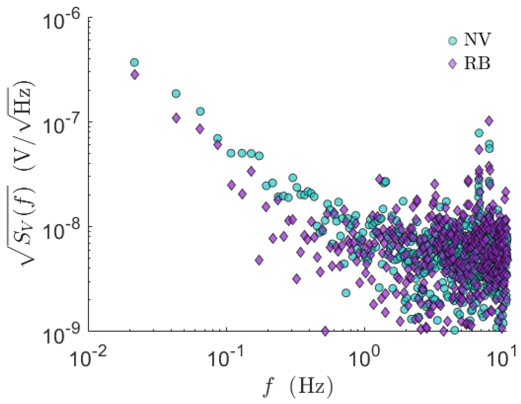
Section 3, the board performances are analyzed, first by characterizing the resistance contacts and relay switching dynamics, including average latency and jitter; second, we evaluate the noise contribution introduced by the switching board when used in series with a nanovoltmeter. Finally, in
Section 4, we propose an experimental validation of the use of the designed board by characterizing an eight-node resistive network connecting two relay matrices in cascade.
2. Relay Board Design and Architecture
This project aims to provide a flexible switching platform that allows any input to be routed to any output. We opted for a single-board solution for a board rather than a modular architecture to obtain a compact, ready-to-use instrument and to minimize additional connectors that could introduce noise. The resulting PCB has a moderate footprint (22 cm × 10 cm) while offering full reconfigurability.
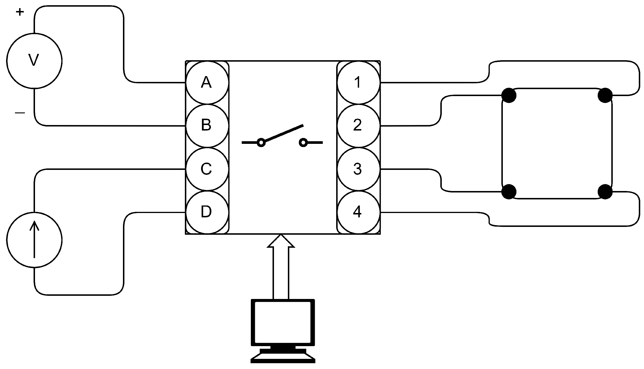
As an example of use, the board can support standard four-probe configurations, including those required by the van der Pauw technique [
18] for sheet-property characterization (see
Figure 1). In this context, the relay matrix allows rapid switching between the measurement geometries needed to extract quantities, such as sheet resistance or Hall voltage, without manually rewiring the sample. Although the van der Pauw method is a convenient illustration, the same routing capabilities enable many other layouts, such as eight-probe anisotropy measurements [
19], alternative Hall geometries, or general purpose test setups. Thanks to the abstract input–output notation of the matrix, each configuration can be described unambiguously and recalled programmatically, allowing automated measurement sequences and complex protocols to be executed with minimal overhead.
In the following, we shall give an overview of the design of the circuit board, its working principles, and its connection with the NUCLEO board [
20].
2.1. Design
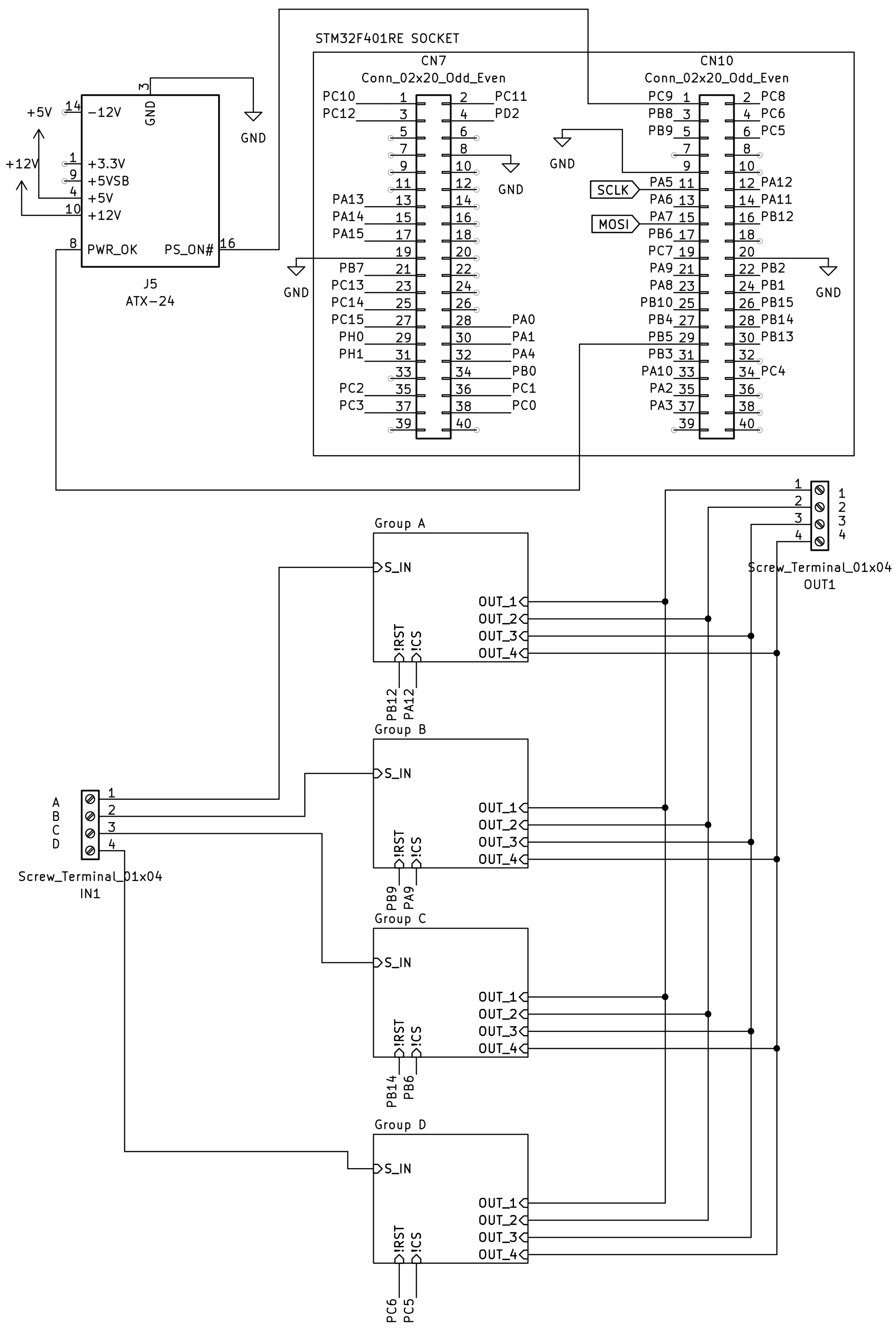
The board adopts a hierarchical structure where each relay group is a ’subsheet’ of the main schematic. This allows the representation of the schematic of the board synthetically, shown in
Figure 2. On the upper part, there are headers that provide the connection to the NUCLEO board, the ATX power supply, and the various relay groups organized as subsheets. Each subsheet is connected to one of the relay board input terminal blocks labeled A, B, C, D and to all the outputs labeled 1, 2, 3, 4. The labels on the
mm female headers follow the NUCLEO board pin numbering, and the ATX connector supplies the 12 V for exciting the coils and powering the relay drivers. The PS_ON pin is intended to turn on/off the ATX power supply, while the PWR_OK reports that all voltages of the power supply have stabilized. The selected driver is the TPL9201 integrated circuit. It is an eight-channel low-side driver designed for controlling inductive or resistive loads such as relays, solenoids, or actuators. It integrates current-limited output stages, protection features, and an internal 5 V regulator, enabling direct interfacing with microcontroller logic. Its SPI control interface minimizes pin usage while providing reliable switching of multiple channels.
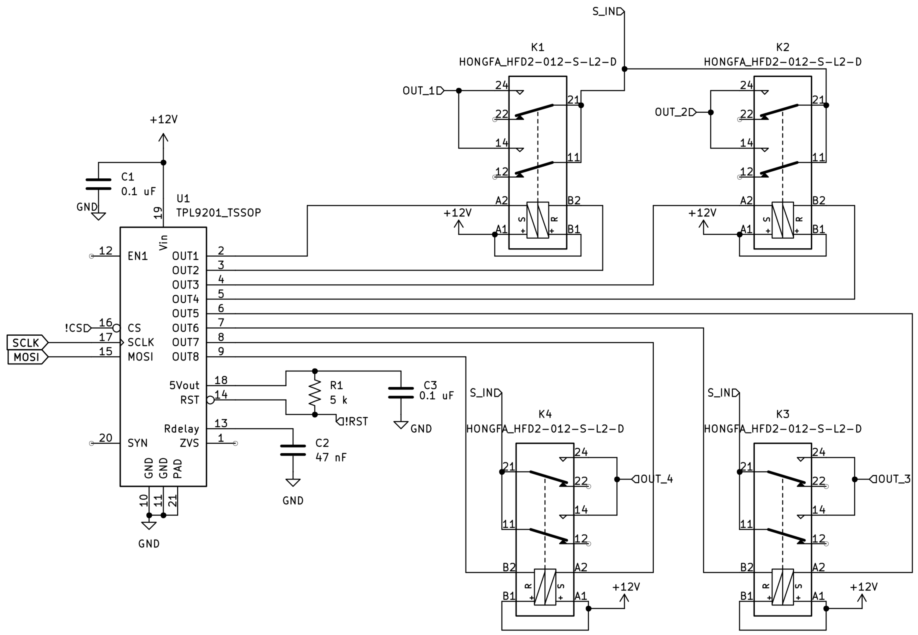
Each relay group (see
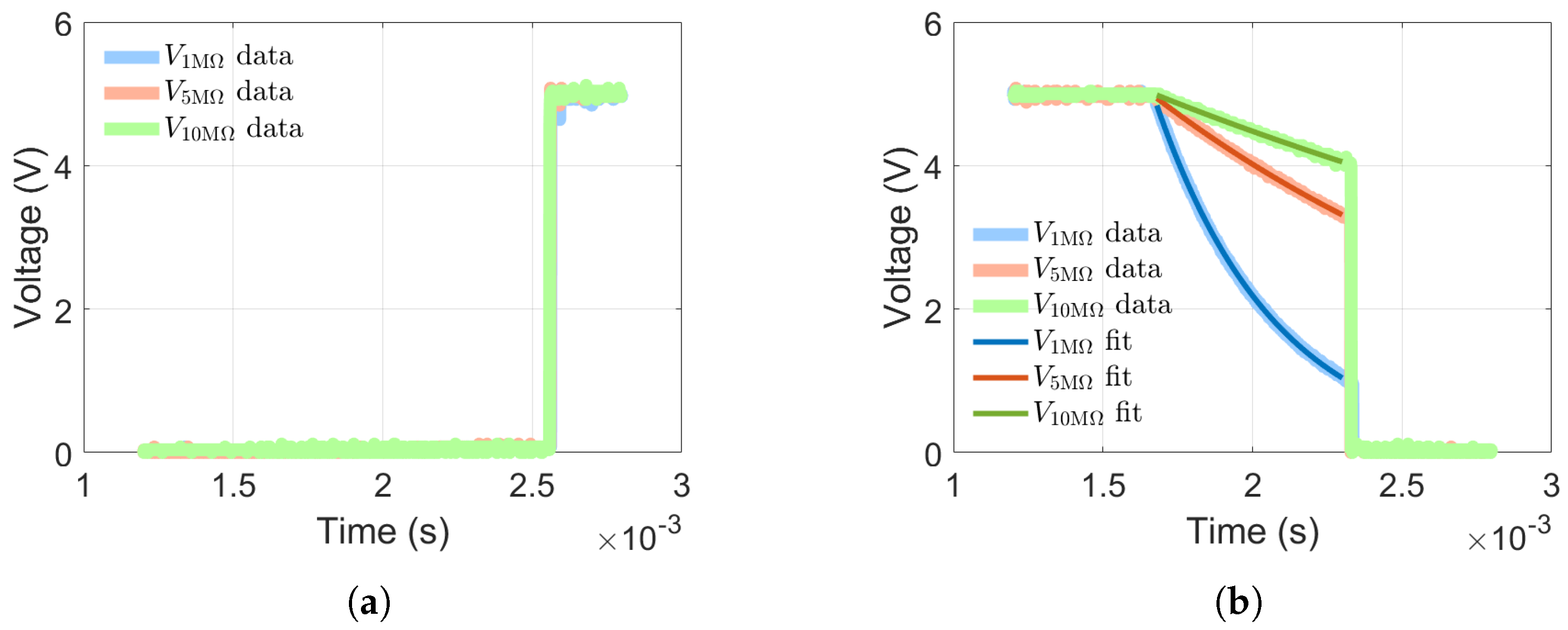
Figure 3), particularly each TPL9201, has an !RST pin; this pin can either be used for resetting the driver (in particular, its stored status byte) by pulling down the associated GPIO, but also reports if the TPL9201 is ready to accept SPI data if it is high. This pin gets sensed before each commute and, if it is low, an error gets reported to the operator; this generally happens when the board is not properly powered. Each subsheet (
Figure 3) illustrates the connections between the TPL9201 driver and the four Hongfa HFD2/012-S-L2-D relays. Since the HFD2 is a bistable dual-coil relay (with separate set and reset coils), each TPL9201 driver controls four relays, corresponding to a total of eight coils.
The PCB has 4 layers and it is built upon the FR4 substrate. The stack-up is as follows:
Each layer has a ground pour with several ground stitching vias across the board. In order to implement a board capable of switching both current and voltage contacts independently on each output position, no specific choices were made regarding dedicated grounding schemes for the current and voltage channels. Furthermore, given the intended application of low-resistance measurements with low currents, leakage currents are negligible. In this configuration, the current and voltage contacts are routed to the sample using a shielded four-wire cable. The cable shield is connected to the board ground; however, this connection is fixed and independent of the switching configuration applied to the individual contacts. If the board were to be adapted for the measurement of resistances >, careful grounding strategies and the implementation of guard potentials would become necessary, requiring the use of triaxial cables up to the device under testing.
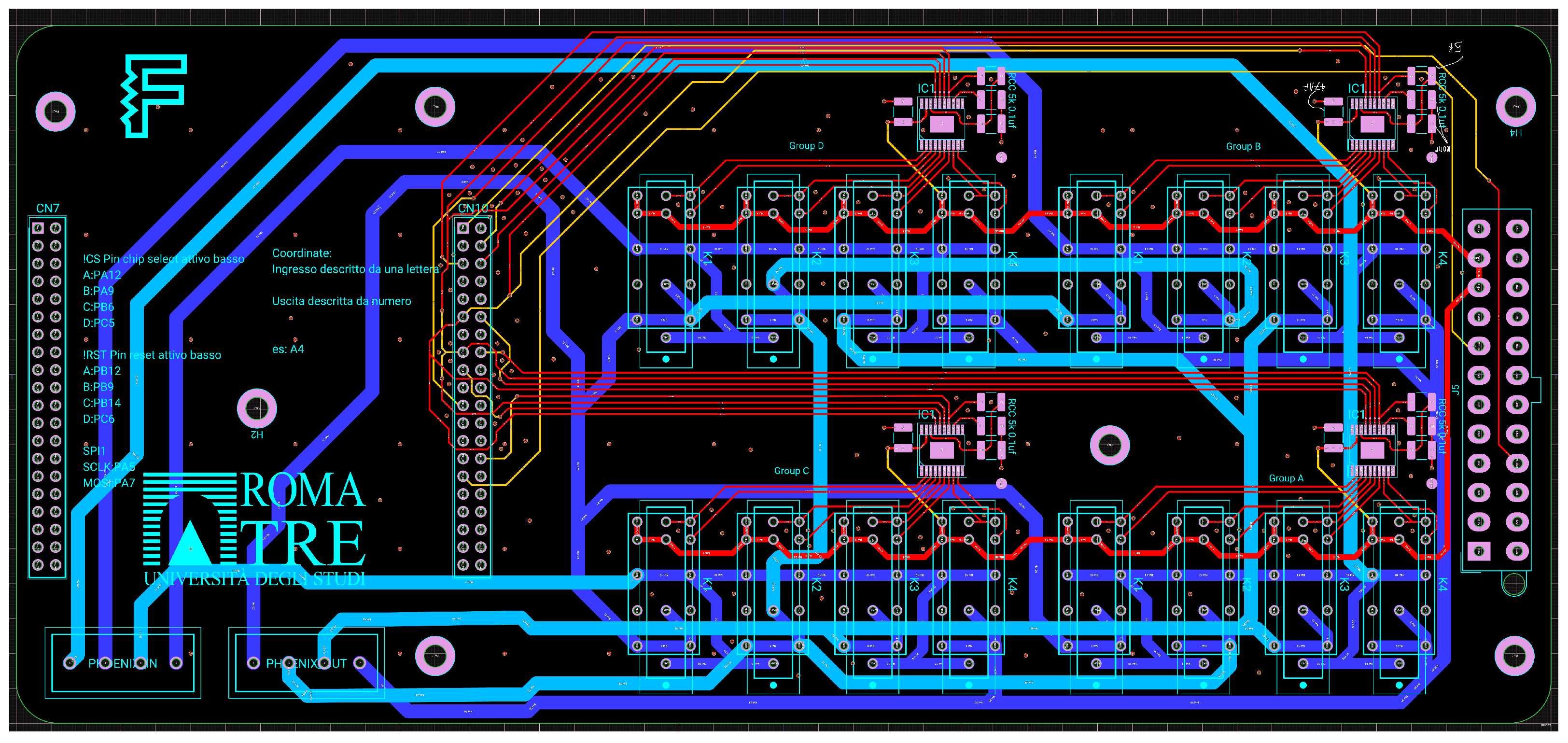
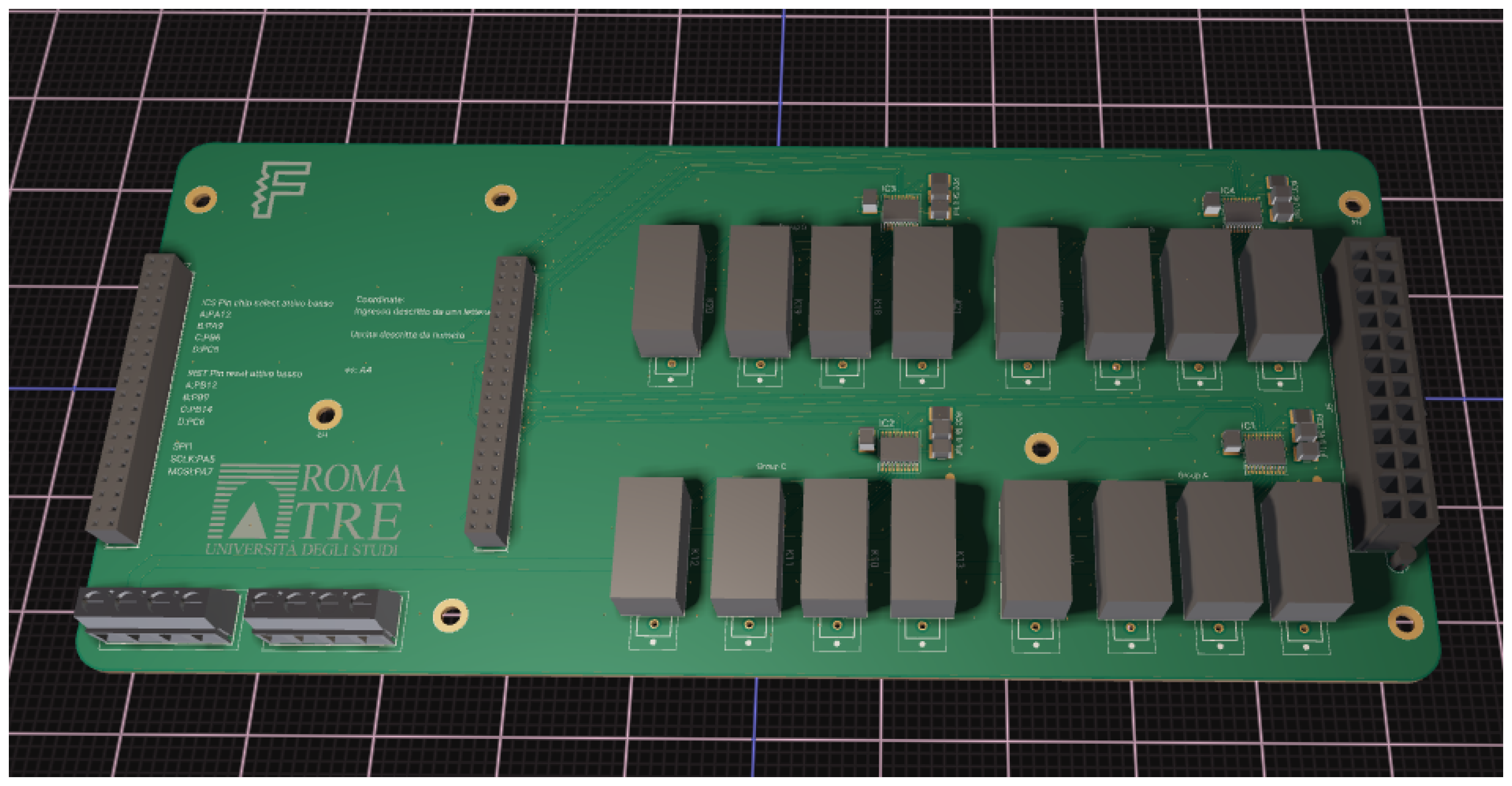
On top of the board, starting from the left (see
Figure 4), there are two different pairs of connectors. The vertically oriented ones are 2 × 20 pin female connectors with a pitch of
mm. The horizontal ones are two 4-pin screw terminals with a pitch of
mm. Both kinds of connectors have through-hole terminals. In this specific implementation, screw terminals were used for instrumentation and sample connections to ensure compatibility with the measurement setups already in use in our laboratory. In these systems, in order to reduce the number of interconnections and improve contact quality, connectors are not employed; instead, continuous cables run directly from the instruments, pass through vacuum-tight feedthroughs into the cryostat, and finally reach the sample. As a result, these cables terminate without connectors, and a screw terminal is the easiest way to connect them without modifying the system. To further improve the board connectivity, the layout can be easily modified to accommodate user-friendly connectors, such as banana plugs or BNC connectors. The NUCLEO board shall be inserted into the
mm headers. In addition, the matrix board also has a few mounting holes. Then the relays are split into four areas. Each area contains four relays, a TPL9201 driver circuit, and various capacitors/resistors that serve the purpose of bypass/pull-up. The footprints of the electromechanical (EMR configuration) and solid-state relays (SSR configuration) overlap, allowing one to choose which kind shall be assembled. On the far right of the board, there is a 24-pin ATX power supply connector, which also allows the monitoring of PWR_OK (voltages stabilized) and PS_ON (on/off ATX power supply) pins, whose purpose was explained earlier, that are specific to the ATX standard. Ideally, a single ATX power supply shall be used for several matrices.
The second layer serves routing purposes; it allows a few SPI-related pins to reach the right-side connector (same orientation in
Figure 4). In fact, the left-side connector only provides additional ground pads. The remaining layers have the purpose of connecting the inputs from the left-side screw terminal (A–D) to all 16 relays and the outputs of the relays to the right-side terminal (1–4). The width of these tracks is 2 mm and allows for currents up to 2 A. No additional vias have been added; thus, layer transitions can only take place at through-hole pads, as shown in
Figure 5.
Due to the low-frequency-oriented design of the presented device, the lack of impedance control and length matching on the signal traces make the board only suitable for signal frequencies from DC to 60 Hz.
2.2. Relay Driving
The operation of the relay control system relies on precise communication between the microcontroller and the TPL9201 driver. The driver manages an array of NMOS transistors which, in turn, control the relays. Understanding how data bytes are transmitted, interpreted, and translated into relay actions is essential for ensuring correct and safe operation, especially considering the differences between solid-state relays (SSRs) and electromagnetic relays (EMRs). The following section details the byte-level communication, the polarization requirements for bistable relays, and the implications for power management and persistence of relay states.
On each commute, a new byte of data gets sent to the TPL9201. The TPL9201 has a 1-byte buffer which allows the control of an array of 8 NMOS transistors in an open-drain configuration. In the SSR version, only half of the byte actually carries the relay group ’status’, which means that 4 transistors of the TPL9201 array are left unused. In the latter, the ’set’ transistors will stay on until a reset is issued, leading to additional power dissipation. This mode of operation is said to be ’monostable’. On the contrary, in the EMR configuration, the whole array is used, implying that the whole byte is relevant. Each pair of coils (so-called set and reset coils) belongs to a relay. These pairs must be polarized in an exclusive way in order to avoid damaging the component. When a group status change gets issued, each relay can be set, reset, or left unchanged. This happens by updating the relevant bits of the TPL buffer; in this case, an even index bit set to one means a set, while an odd index one implies a reset (counting from the LSB). After a certain amount of time specified from the HFD2 datasheet, which grants that the commutation is completed, the whole transistor array is switched off. While in the SSR configuration, this would have resulted in an entire group being reset, in the EMR configuration, the relays are persistent in both statuses. This means that the board 12 V supply may be switched off using the PS_ON pin and all the connections would persist. In the following, we will focus on the EMR configuration.
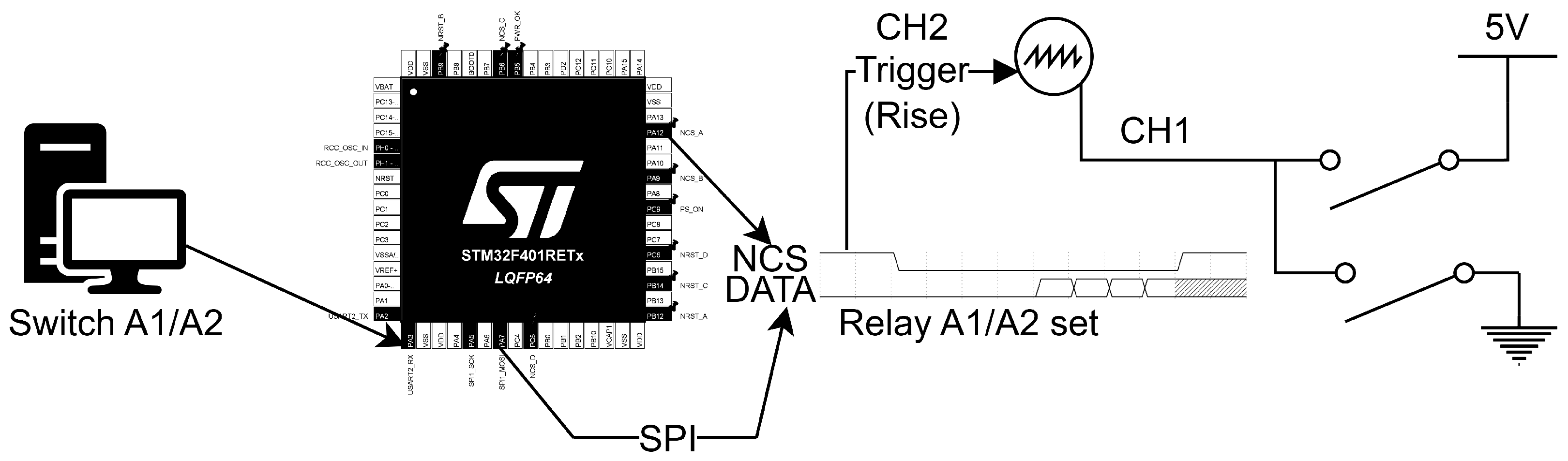
In
Figure 6, there is an example update of a specific group. While the NCS signal selects a specific TPL, DATA will determine which relays have to be set (S) or reset (R). The first number identifies a specific relay (1–4), and the second letter specifies which coil will be energized (set or reset). Each pair of bits of the said byte must have at least one zero in order to avoid simultaneously polarizing the two coils, damaging the relay.
After the latching time, the NCS is pulled down and a null byte gets sent in order to turn off the whole transistor array; as the relays are bistable, there is no need to keep the coils energized.
2.3. Firmware
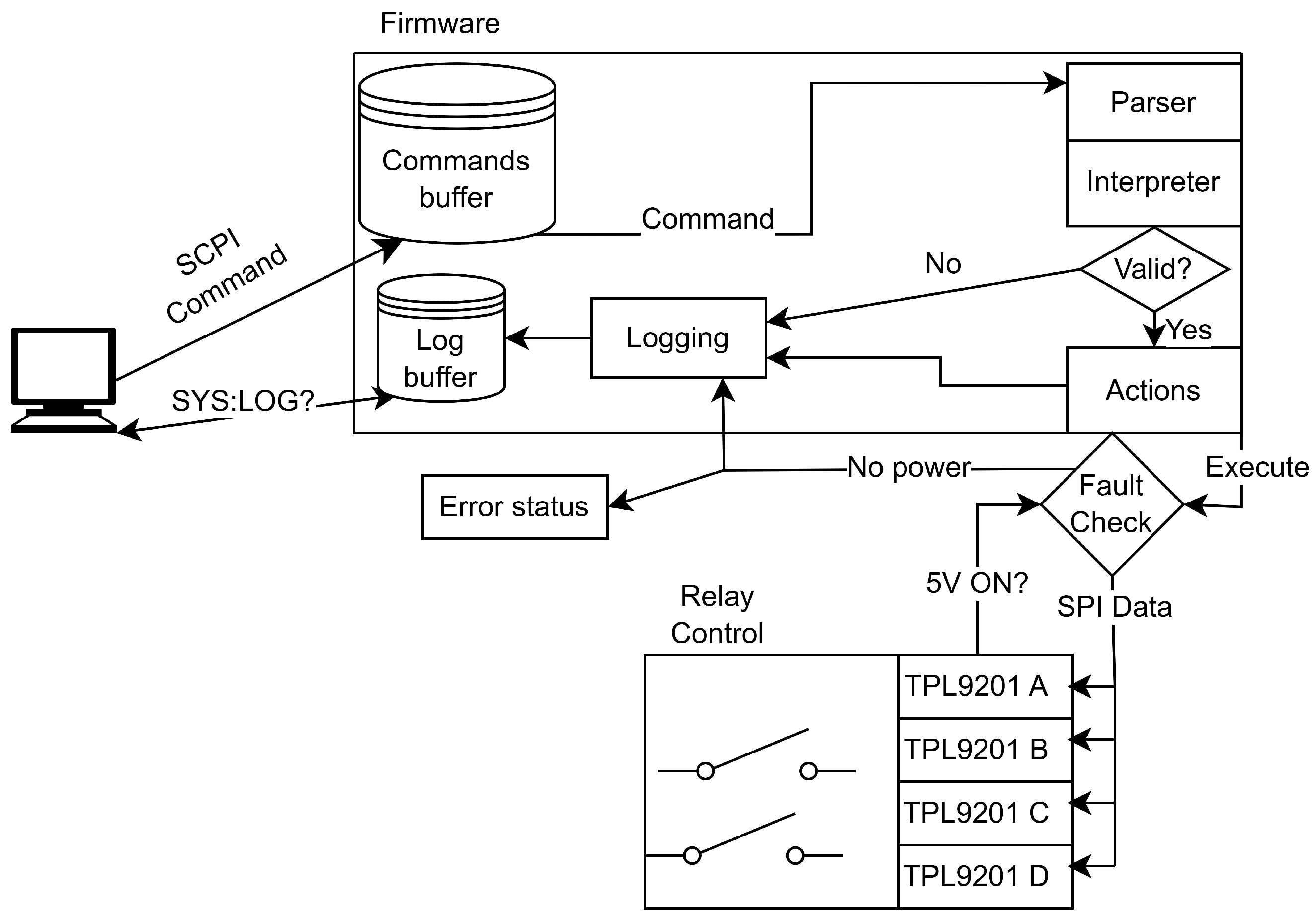
The firmware of the STM32F401RE board, which controls the matrix, is based on the Hardware Abstraction Layer (HAL). Its aim is both to send data to all TPL9201 and provide a basic serial interface which is heavily inspired by SCPI (Standard Commands for Programmable Interface) syntax. The microcontroller exposes a UART port using the only USB connector the board has as a COM port, making any modern operating system capable of detecting it. Each received command is stored in a memory area using a Direct Memory Access (DMA) peripheral; then, an interrupt event is generated and subsequently served by the microcontroller. The interrupt callback ends when the command string gets added to a linked list. During each iteration, the finite state machine (FSM) loop checks if there are any commands that are waiting to get processed. If the list is not empty, then the command in its raw form gets parsed by the parser component and a command structure gets associated to it; this instance gets put in another list. The interpreter will then check if the command is valid and eventually execute the associated action.
After the execution, a log string gets populated with basic information on whether the action was successful, data returned, errors, etc. The contents of the latter may be obtained with a dedicated query. In
Figure 7, the flow chart of the firmware operation is shown.
4. Experimental Validation
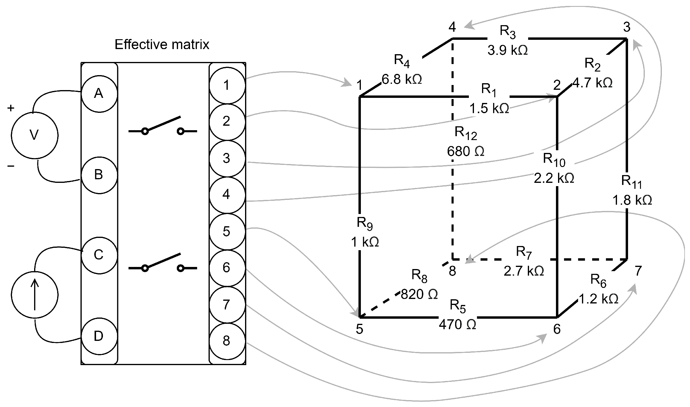
To demonstrate the modularity and scalability of the switching system, we cascaded two 4 × 4 relay boards, effectively producing an eight-channel reconfigurable switching matrix. As a testbench, we constructed a three-dimensional resistive network in the form of a cube with twelve independently chosen resistances, one for each edge, as depicted in
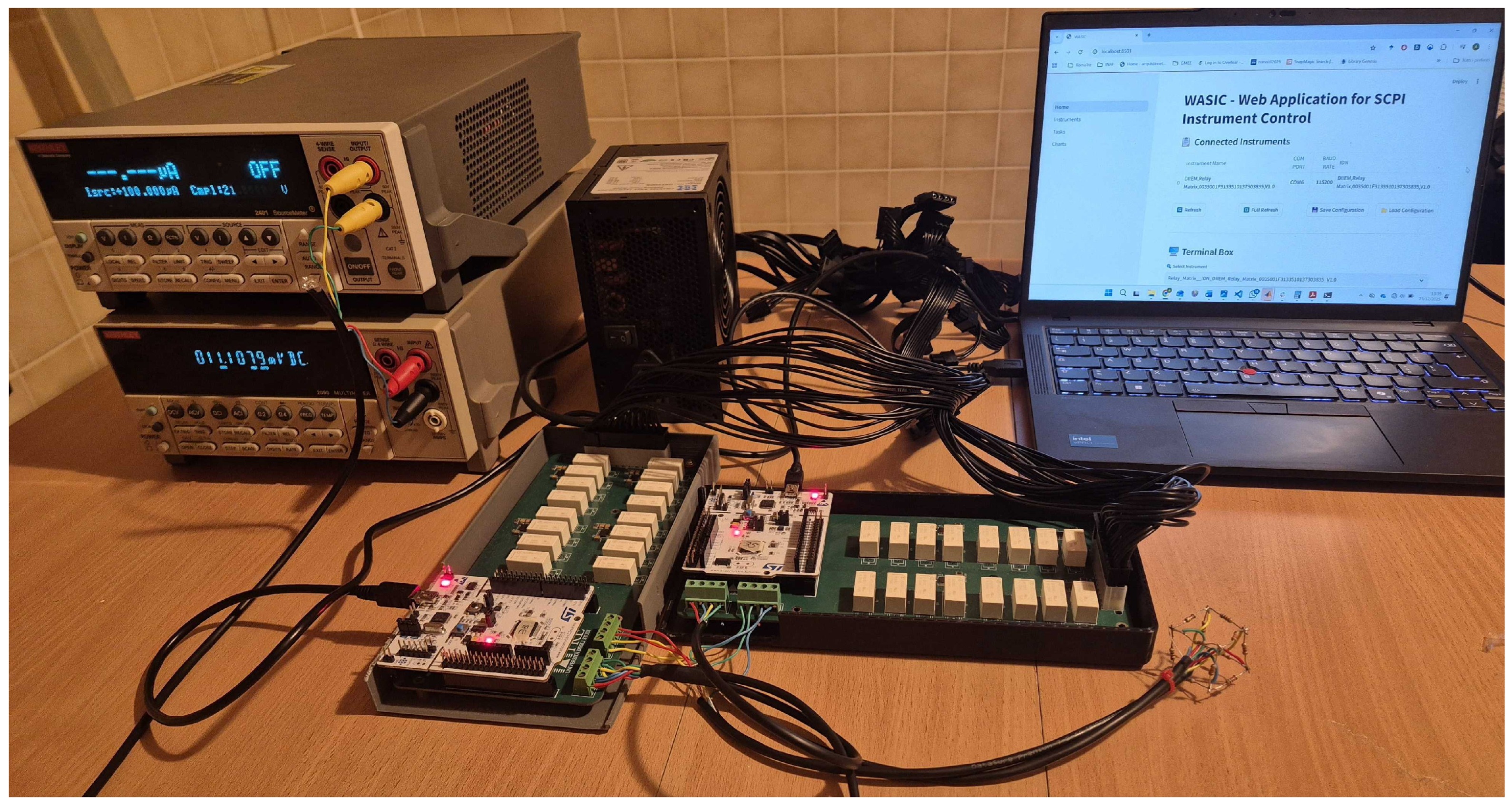
Figure 14 and shown in
Figure 15. The routing system allows arbitrary selection of the current injection pair and of the voltage measurement pair, enabling a complete four-terminal characterization of the network without any manual rewiring.
A four-terminal measurement on an
N-node resistive network is completely determined by (i) a pair of nodes used for current injection and extraction, and (ii) a second pair of nodes used for voltage sensing. In our case,
. Each pair is an unordered two-element subset of the node set. For the current terminals, the unordered nature follows from the fact that exchanging the two nodes merely inverts the sign of the injected current vector. When the voltage terminals are exchanged simultaneously, the measured differential voltage changes signs as well, leaving the corresponding four-terminal resistance
unchanged in magnitude. Thus, the measurement is physically identical under the exchange
and
, and each terminal pair is combinatorially a set rather than an ordered tuple. The number of admissible current pairs is the number of two-element subsets of eight nodes
. Once the current terminals
are chosen, they cannot be reused as voltage terminals; hence, the voltage pair must be chosen among the remaining six nodes
. Since the two choices are independent, the total number of physically distinct four-terminal measurements is
This enumeration counts only genuinely different measurements, excluding all permutations that lead to sign changes but not to new physical information.
The cube network consists of eight nodes and twelve resistive edges. The adopted numbering is shown in
Figure 14. Let
denote the conductance of edge
k. The nodal admittance matrix of the cube is an
sparse symmetric matrix:
The nodal voltages follow from
where
is the current injection vector. The twelve edge resistances of the cube are reconstructed from the complete set of 420 four-terminal measurements. To guarantee positivity of the parameters and to improve the numerical conditioning of the inverse problem, the optimization is carried out using a logarithmic parametrization of the conductances:
The logarithmic parametrization improves the robustness of the nonlinear fit by enforcing
exactly and reducing the effective dynamic range of the parameters. For a given configuration of current injection nodes
and voltage-sensing nodes
, the theoretical four-terminal equivalent resistance is computed from the nodal equation
(see Equation (
3)) as
where
is the excitation current and
and
are the voltages at nodes C and D, obtained after solving the nodal system.
We used a Keithley 2400 SMU (Keithley Instruments LLC, Solon, OH, USA) as a current source (set to mA) and a Keithley 2000 DMM (Keithley Instruments LLC, Solon, OH, USA) as a differential voltmeter for these validation measurements. Each measurement is acquired twice, once with and once with , and the two values are averaged. This current-reversal technique suppresses thermoelectric offsets.
To reconstruct conductance values, we performed a minimization of a Tikhonov-regularized objective function [
24]:
where
is the vector of measured four-terminal resistances,
is a prior estimate, and
is the regularization parameter that controls the weight of the prior estimate. After minimization, the fitted resistances are obtained as
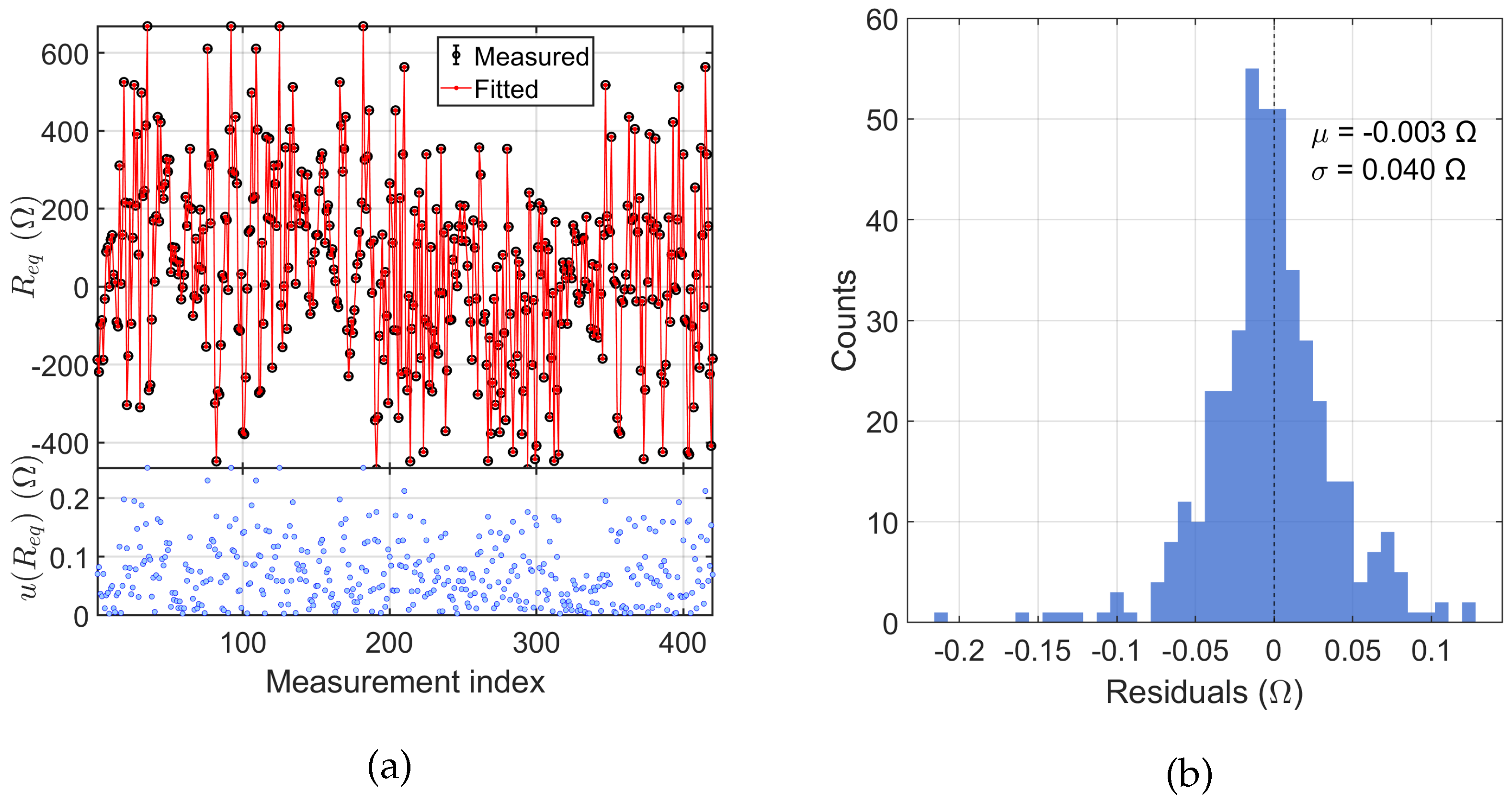
The comparison between the measured
y and fitted
values, together with the distribution of the residuals, are shown in
Figure 16. The uncertainties were calculated based on the accuracy of the set value on the current source (10 mA) and the accuracy of the voltage measurements. Voltage measurements were performed with the instrument in autorange mode to ensure optimal resolution for each point. Depending on the measured voltage, the instrument automatically switches between 100 mV, 1 V, and 10 V ranges. The uncertainties for each measurement were then evaluated according to the specifications reported in the instrument datasheet for the corresponding range. Since the residuals shown in
Figure 16 are centered around
, the presence of systematic offset errors introduced by the designed board can be excluded within the measurement uncertainty. While a gain error cannot be ruled out in principle, its introduction by the board is highly unlikely, as the system is entirely passive and does not include any amplification/attenuation stages. These observations indicate that the switching platform does not compromise the measurement trueness, which remains determined by the intrinsic performance of the current source and the voltmeter used in the experiment.
5. Conclusions
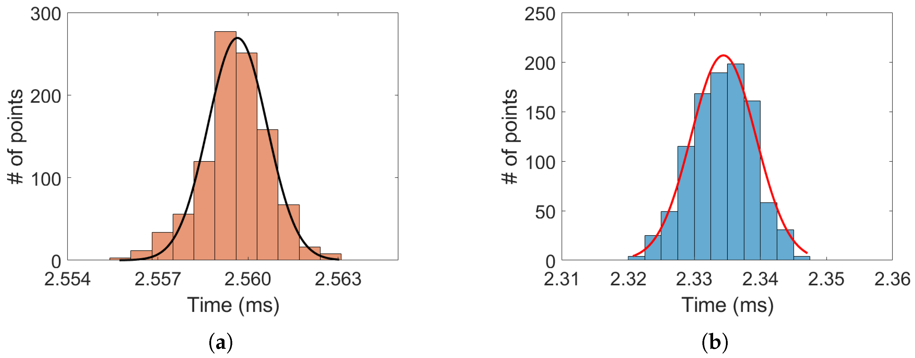
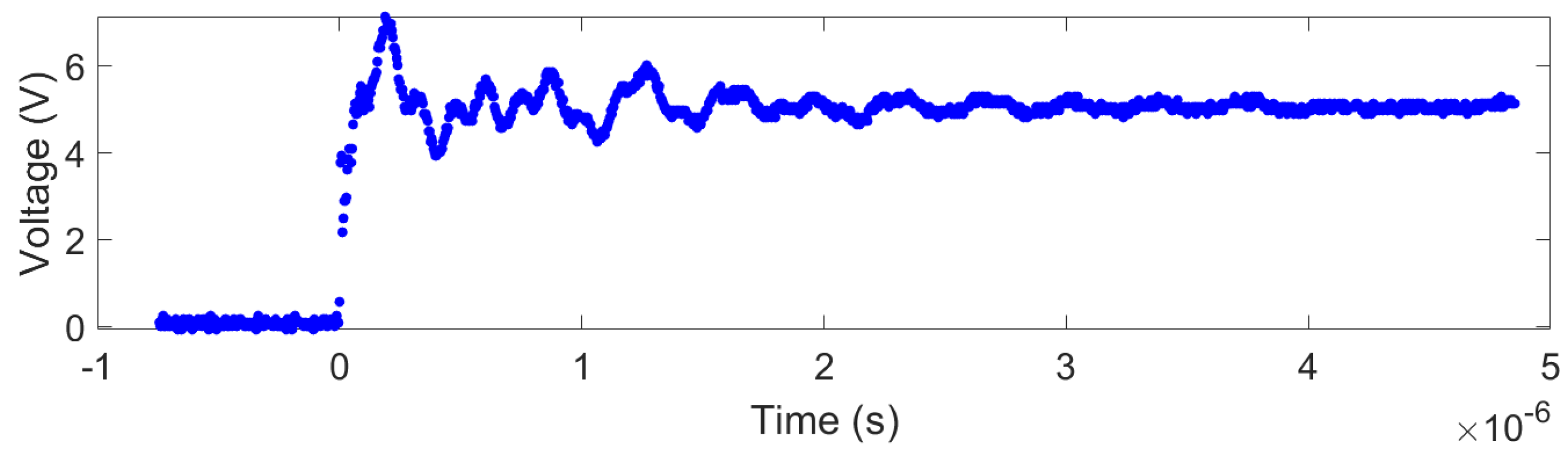
We have experimentally demonstrated that the proposed relay-based switching platform represents a viable and effective solution for automated DC measurements requiring flexible signal routing, low noise, and modular scalability. The characterization of the switching dynamics revealed a clear asymmetry between closing and opening transitions, with closing times ms and slightly longer times ms for opening transitions. This behavior is consistent with the presence of small parasitic capacitances at the relay contacts and PCB level. A simple RC model yields an effective capacitance of approximately 350 pF, in good agreement with typical relay and layout parasitic contributions. Importantly, the measured switching jitter, estimated as standard deviation of the closing and opening times, remained below , ensuring excellent timing reproducibility even in fast automated measurement sequences. From a noise perspective, the board introduces no measurable degradation of nanovoltmeter performance within the experimental sensitivity. Both the low-frequency noise behavior and the high-frequency white-noise floor are preserved, demonstrating that the selected bistable relays and compact PCB layout do not introduce additional pickup or dynamic noise beyond the intrinsic limits of the measurement instrumentation.
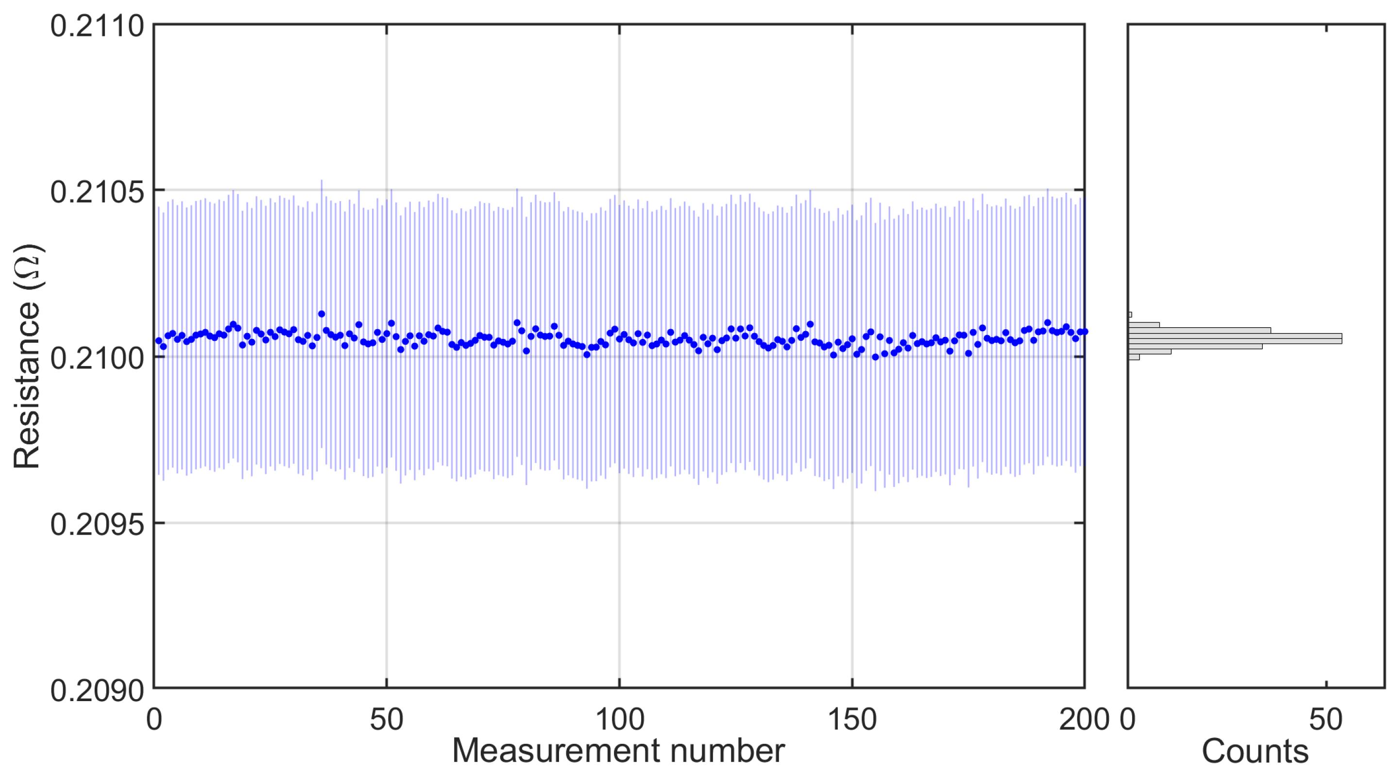
A key motivation for the development of this platform is its application to low-resistance measurements, which represent one of the most challenging use cases for automated switching systems. In this context, the main potential sources of systematic error, contact resistance, and thermoelectric potentials were carefully considered. The contact resistance introduced by the board was measured to be ∼
, a value significantly lower than that of many commercial switching solutions and, importantly, smaller than the typical resistances encountered in cryogenic wiring and sample leads. Such contributions are fully compensated by standard four-wire (4 W) measurement techniques. Thermoelectric potentials, which are unavoidable in low-resistance DC measurements, can be effectively mitigated using well-established current-reversal methods [
10]. These can be implemented either through current sources capable of polarity inversion or by rapidly switching the current contacts while leaving the voltage contacts untouched. The fast switching times achieved by the chosen relays, on the order of a few milliseconds, are negligible when compared to the integration times of nanovoltmeters commonly employed in these applications, which are typically on the order of seconds. Together with the low switching jitter, this ensures precise control of measurement timing and reliable implementation of multi-point current-reversal schemes. As a result, the proposed board does not introduce systematic errors or noise contributions larger than those already present in typical cryogenic measurement setups, and all residual effects are fully compensable within the typical measurement accuracies that are reached in these applications, using standard measurement protocols. Consequently, micro-ohm resolution can be reliably achieved even with bias currents below 10 mA, and the measurement accuracy is fully determined by the performance of the current source and nanovoltmeter used rather than by the switching platform itself.
Finally, the case study involving a three-dimensional resistive network highlights the scalability of the system. By cascading two units to form an eight-channel matrix, a complete set of 420 four-terminal measurements was performed without manual rewiring, enabling automated reconstruction of the network’s resistive distribution. This demonstrates that the platform successfully balances measurement accuracy, hardware simplicity, scalability, and acquisition speed. Overall, the combination of predictable switching behavior, low noise, and inherent modularity makes the proposed system a powerful open-hardware tool for automated electrical measurements, which can be used with different kinds of measurement instruments and is particularly well suited for low-resistance applications.