Engineering Porous Silicon Nanowires with Tuneable Electronic Properties

 , ,
, ,  ,
,  and
and
Abstract
1. Introduction
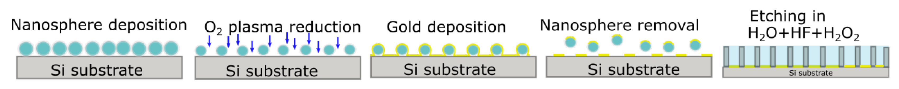
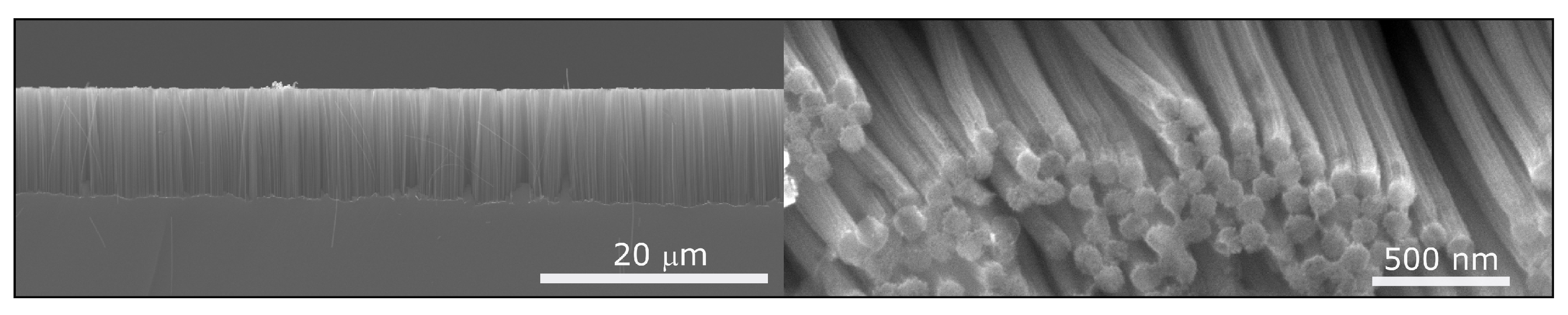
2. Experimental
3. Results and Discussion
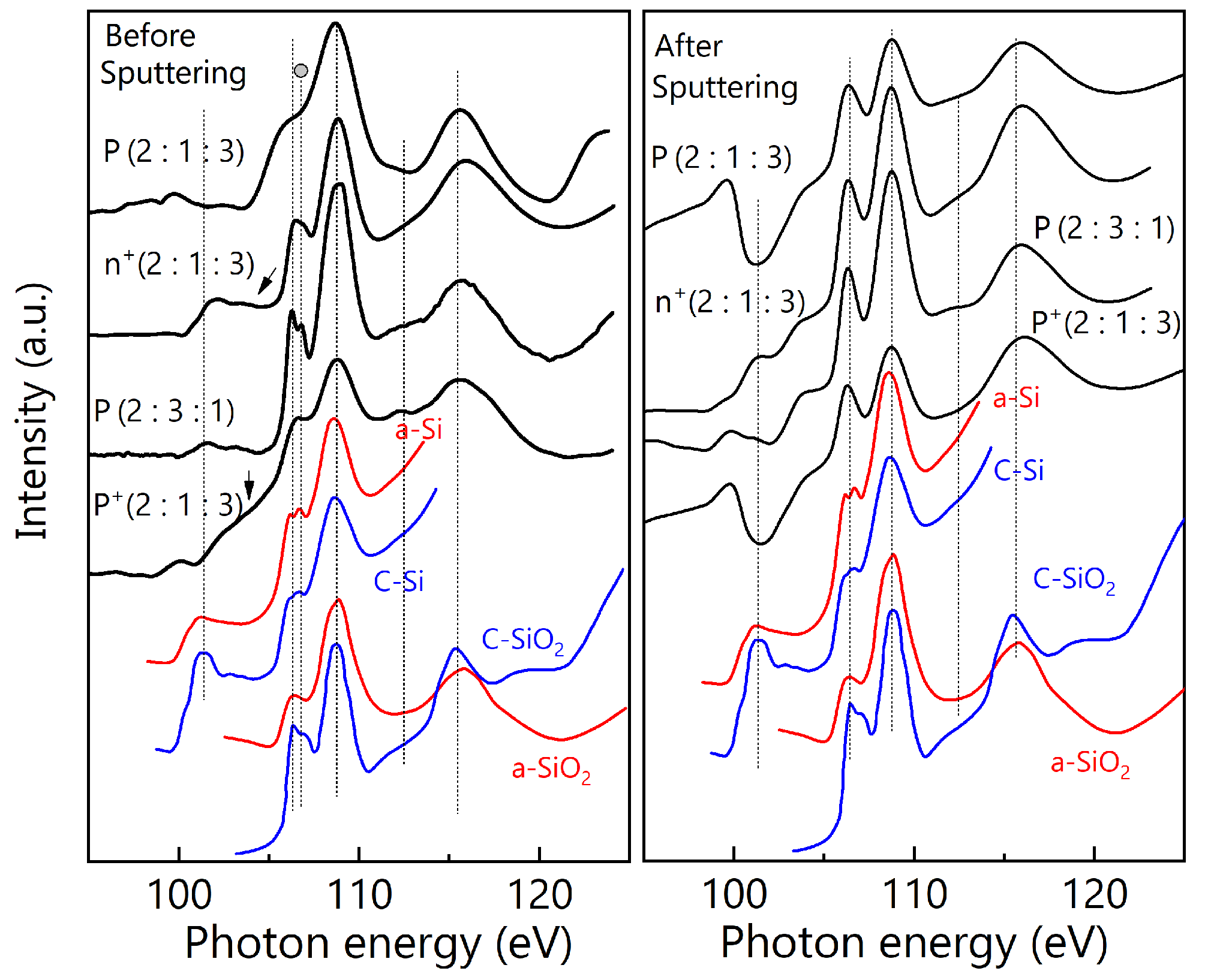
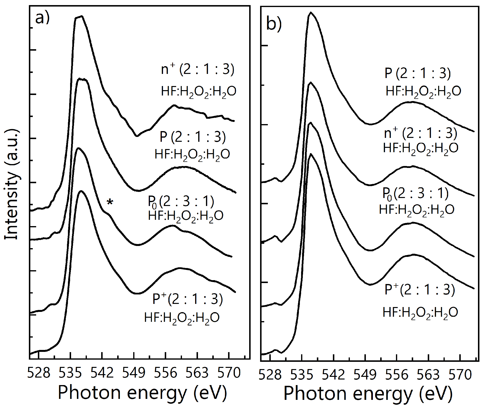
3.1. X-ray Absorption Spectroscopy
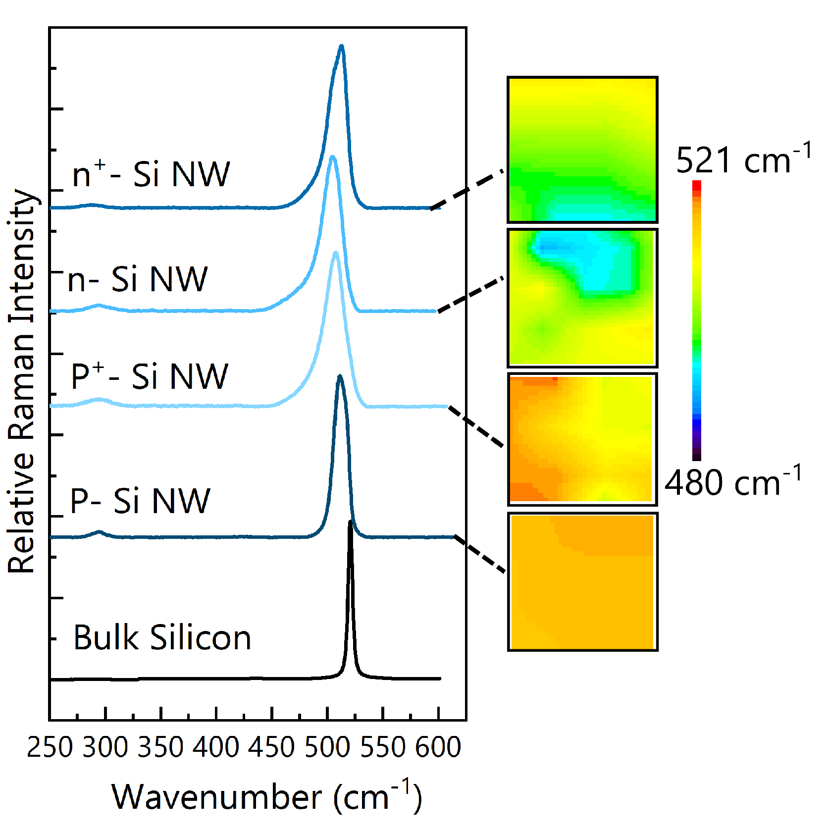
3.2. Raman Spectroscopy
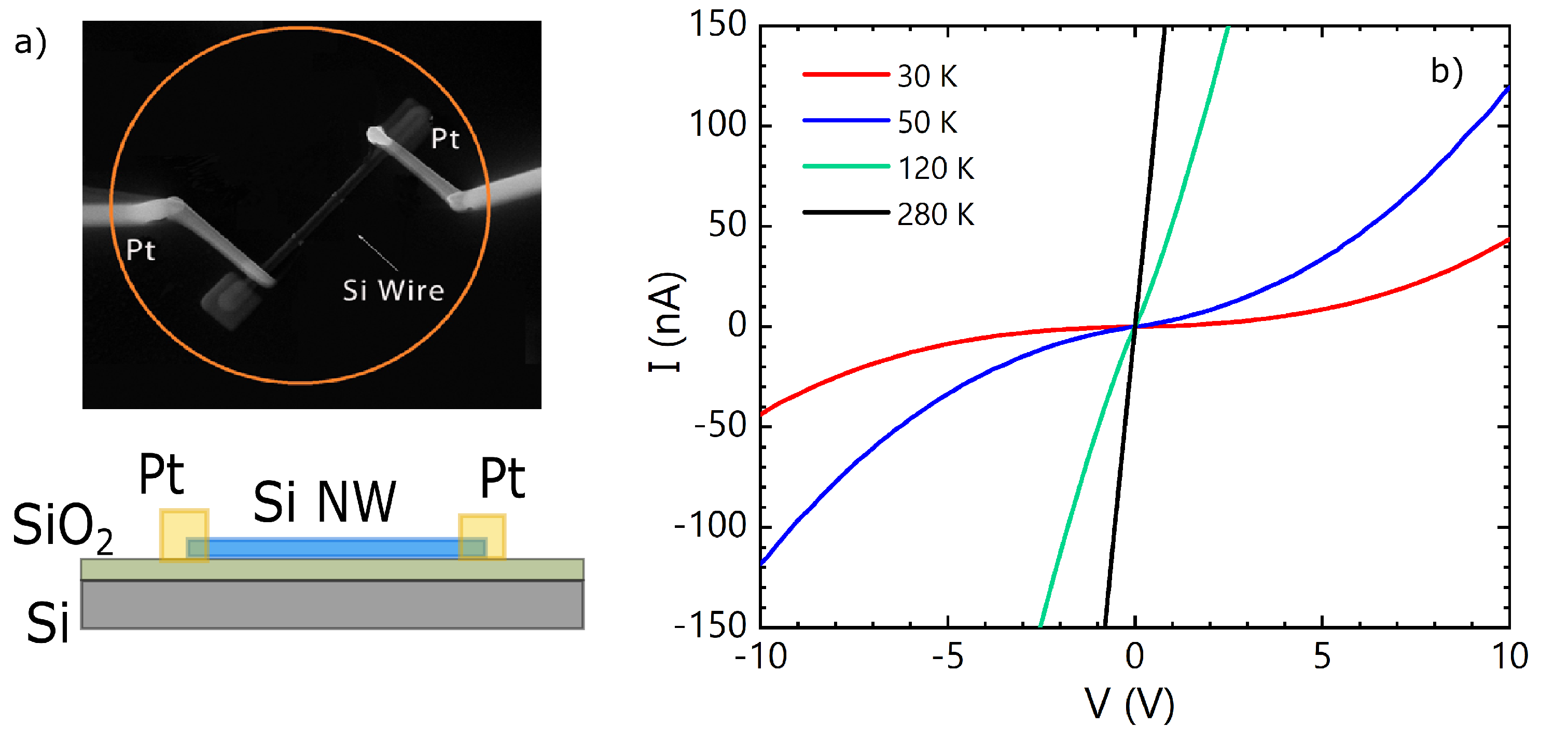
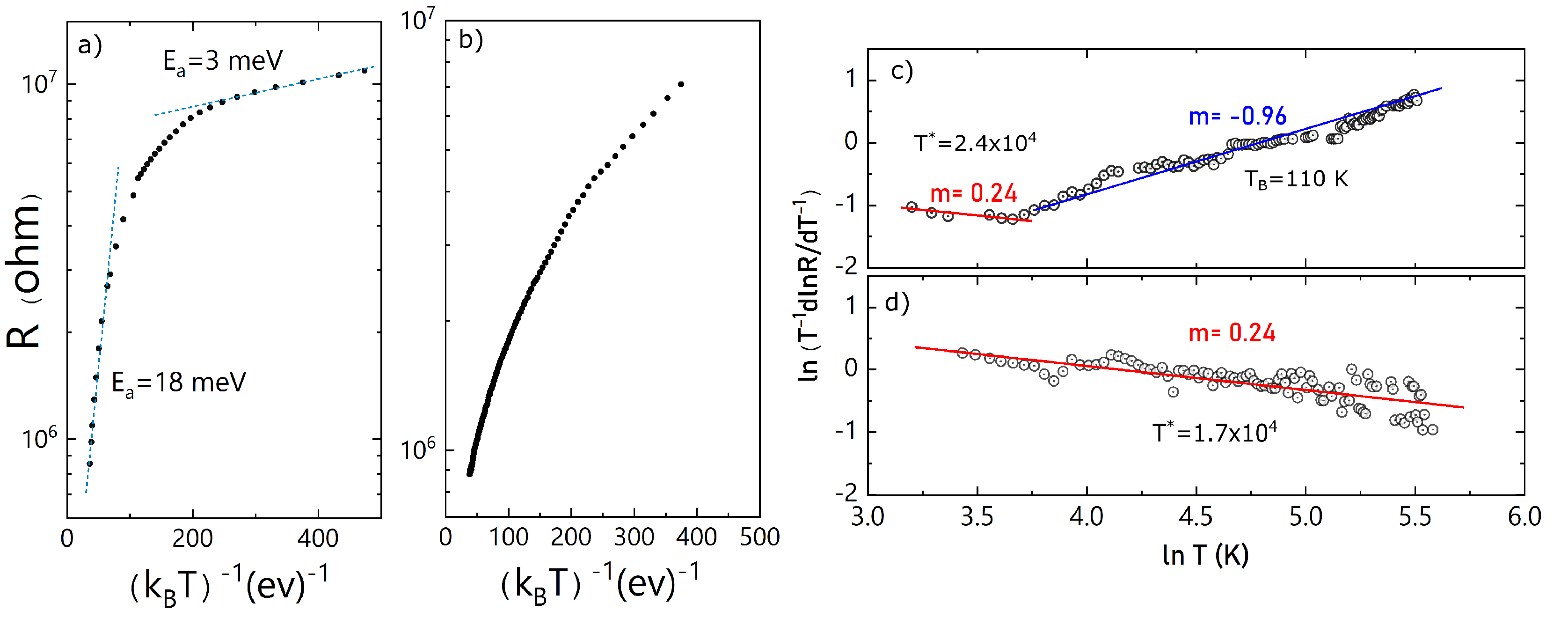
3.3. Charge Carrier Transport
4. Conclusions
Author Contributions
Funding
Conflicts of Interest
References
- Canham, L.T. Silicon quantum wire array fabrication by electrochemical and chemical dissolution of wafers. Appl. Phys. Lett. 1990, 57, 1046–1048. [Google Scholar] [CrossRef]
- Kang, Z.; Tsang, C.; Wong, N.; Zhang, Z.; Lee, S. Silicon Quantum Dots: A General Photocatalyst for Reduction, Decomposition, and Selective Oxidation Reactions. J. Am. Chem. Soc. 2007, 129, 12090–12091. [Google Scholar] [CrossRef] [PubMed]
- Pavesi, L.; Dal Negro, L.; Mazzoleni, C.; Franzo, G.; Priolo, F. Optical gain in silicon nanocrystals. Nature 2000, 408, 440–444. [Google Scholar] [CrossRef] [PubMed]
- D’Elia, A.; Cepek, C.; de Simone, M.; Macis, S.; Belec, B.; Fanetti, M.; Piseri, P.; Marcelli, A.; Coreno, M. Interplay among work function, electronic structure and stoichiometry in nanostructured VO x films. Phys. Chem. Chem. Phys. 2020, 22, 6282–6290. [Google Scholar] [CrossRef] [PubMed]
- Lehmann, V.; Gosele, U. Porous silicon formation: A quantum wire effect. Appl. Phys. Lett. 1991, 58, 856–858. [Google Scholar] [CrossRef]
- Borini, S.; Boarino, L.; Amato, G. Coulomb blockade tuned by NO2 molecules in nanostructured silicon. Adv. Mater. 2006. [Google Scholar] [CrossRef]
- Loni, A.; Defforge, T.; Caffull, E.; Gautier, G.; Canham, L. Porous silicon fabrication by anodisation: Progress towards the realisation of layers and powders with high surface area and micropore content. Microporous Mesoporous Mater. 2015, 213, 188–191. [Google Scholar] [CrossRef]
- Carturan, S.; Maggioni, G.; Rezvani, S.; Gunnella, R.; Pinto, N.; Gelain, M.; Napoli, D. Wet chemical treatments of high purity Ge crystals for γ-ray detectors: Surface structure, passivation capabilities and air stability. Mater. Chem. Phys. 2015, 161, 116–122. [Google Scholar] [CrossRef]
- Deng, M.T.; Yu, C.L.; Huang, G.Y.; Larsson, M.; Caroff, P.; Xu, H.Q. Anomalous zero-bias conductance peak in a Nb-InSb nanowire-Nb hybrid device. Nano Lett. 2012. [Google Scholar] [CrossRef]
- Nilsson, H.A.; Samuelsson, P.; Caroff, P.; Xu, H.Q. Supercurrent and Multiple Andreev Reflections in an InSb Nanowire Josephson Junction. Nano Lett. 2012, 12, 228–233. [Google Scholar] [CrossRef]
- Pasqualini, M.; Calcaterra, S.; Maroni, F.; Rezvani, S.; Cicco, A.D.; Alexander, S.; Rajantie, H.; Tossici, R.; Nobili, F. Electrochemical and spectroscopic characterization of an alumina-coated LiMn2O4 cathode with enhanced interfacial stability. Electrochim. Acta 2017, 258, 175–181. [Google Scholar] [CrossRef]
- Rezvani, S.; Pasqualini, M.; Witkowska, A.; Gunnella, R.; Birrozzi, A.; Minicucci, M.; Rajantie, H.; Copley, M.; Nobili, F.; Cicco, A.D. Binder-induced surface structure evolution effects on Li-ion battery performance. Appl. Surf. Sci. 2018, 435, 1029–1036. [Google Scholar] [CrossRef]
- Pinto, N.; Rezvani, S.J.; Perali, A.; Flammia, L.; Milošević, M.V.; Fretto, M.; Cassiago, C.; De Leo, N. Dimensional crossover and incipient quantum size effects in superconducting niobium nanofilms. Sci. Rep. 2018, 8, 4710. [Google Scholar] [CrossRef] [PubMed]
- Rezvani, S.J.; Gioacchino, D.D.; Gatti, C.; Ligi, C.; Guidi, M.C.; Cibella, S.; Fretto, M.; Poccia, N.; Lupi, S.; Marcelli, A. Proximity Array Device: A Novel Photon Detector Working in Long Wavelengths. Condens. Matter 2020, 5, 33. [Google Scholar] [CrossRef]
- Rezvani, S.J.; Gunnella, R.; Neilson, D.; Boarino, L.; Croin, L.; Aprile, G.; Fretto, M.; Rizzi, P.; Antonioli, D.; Pinto, N. Effect of carrier tunneling on the structure of Si nanowires fabricated by metal assisted etching. Nanotechnology 2016. [Google Scholar] [CrossRef]
- Rezvani, S.J.; Pinto, N.; Boarino, L. Rapid formation of single crystalline Ge nanowires by anodic metal assisted etching. CrystEngComm 2016, 18, 7843–7848. [Google Scholar] [CrossRef]
- Wagner, R.S.; Ellis, W.C. Vapor-Liquid-Solid Mechanism of Single Crystal Growth. Appl. Phys. Lett. 1964, 4, 89. [Google Scholar] [CrossRef]
- Pinto, N.; Rezvani, S.J.; Favre, L.; Berbezier, I.; Fretto, M.; Boarino, L. Geometrically induced electron-electron interaction in semiconductor nanowires. Appl. Phys. Lett. 2016. [Google Scholar] [CrossRef]
- Rezvani, S.J.; Pinto, N.; Boarino, L.; Celegato, F.; Favre, L.; Berbezier, I. Diffusion induced effects on geometry of Ge nanowires. Nanoscale 2014, 6, 7469–7473. [Google Scholar] [CrossRef]
- Rezvani, S.J.; Favre, L.; Celegato, F.; Boarino, L.; Berbezier, I.; Pinto, N. Supersaturation state effect in diffusion induced Ge nanowires growth at high temperatures. J. Cryst. Growth 2016. [Google Scholar] [CrossRef]
- BEAR Beamline, IOM-CNR. Available online: https://www.elettra.trieste.it/it/lightsources/elettra/elettra-beamlines/bear/bear.html (accessed on 15 July 2018).
- Turishchev, S.Y.; Parinova, E.V.; Pisliaruk, A.K.; Koyuda, D.A.; Yermukhamed, D.; Ming, T.; Ovsyannikov, R.; Smirnov, D.; Makarova, A.; Sivakov, V. Surface deep profile synchrotron studies of mechanically modified top-down silicon nanowires array using ultrasoft X-ray absorption near edge structure spectroscopy. Sci. Rep. 2019, 9, 8066. [Google Scholar] [CrossRef] [PubMed]
- Li, D.; Bancroft, G.M.; Kasrai, M.; Fleet, M.; Secco, R.; Feng, X.; Tang, K.; Yang, B.X. X-ray absorption spectroscopy of silicon dioxide (SiO2) polymorphs: The structural characterization of opal. Am. Mineral. 1994, 79, 622–632. [Google Scholar]
- Harp, G.R.; Han, Z.L.; Tonner, B.P. Spatially-resolved X-ray Absorption Near-edge Spectroscopy of Silicon in Thin Silicon-oxide Films. Phys. Scr. 1990. [Google Scholar] [CrossRef]
- Himpsel, F.J.; McFeely, F.R.; Taleb-Ibrahimi, A.; Yarmoff, J.A.; Hollinger, G. Microscopic structure of the SiO2/Si interface. Phys. Rev. B 1988, 38, 6084–6096. [Google Scholar] [CrossRef] [PubMed]
- Harp, G.R.; Han, Z.L.; Tonner, B.P. X-ray absorption near edge structures of intermediate oxidation states of silicon in silicon oxides during thermal desorption. J. Vac. Sci. Technol. A Vac. Surf. Films 1990. [Google Scholar] [CrossRef]
- Turishchev, S.; Terekhov, V.; Parinova, E.; Korolik, O.; Mazanik, A.; Fedotov, A. Surface modification and oxidation of Si wafers after low energy plasma treatment in hydrogen, helium and argon. Mater. Sci. Semicond. Process. 2013, 16, 1377–1381. [Google Scholar] [CrossRef]
- Li, B.; Yu, D.; Zhang, S.L. Raman spectral study of silicon nanowires. Phys. Rev. B 1999, 59, 1645–1648. [Google Scholar] [CrossRef]
- Siu, G.G.; Wu, X.L.; Gu, Y.; Bao, X.M. Ultraviolet and blue emission from crystalline SiO2 coated with LiNbO3 and LiTaO3. Appl. Phys. Lett. 1999, 74, 1812–1814. [Google Scholar] [CrossRef]
- Khorasaninejad, M.; Walia, J.; Saini, S.S. Enhanced first-order Raman scattering from arrays of vertical silicon nanowires. Nanotechnology 2012, 23, 275706. [Google Scholar] [CrossRef]
- Zhang, S.; Wang, X.; Ho, K.; Li, J.; Diao, P.; Cai, S. Raman spectra in a broad frequency region of p type porous silicon. J. Appl. Phys. 1994, 76, 3016–3019. [Google Scholar] [CrossRef]
- D’Ortenzi, L.; Monsù, R.; Cara, E.; Fretto, M.; Kara, S.; Rezvani, S.J.; Boarino, L. Electrical Contacts on Silicon Nanowires Produced by Metal-Assisted Etching: A Comparative Approach. Nanoscale Res. Lett. 2016, 11, 468. [Google Scholar] [CrossRef] [PubMed]
- Zabrodskii, A. Electrical conductivity of heavily doped compensated n-type germanium produced by neutron doping. Sov. Phys. Semicond. 1980, 14, 670–676. [Google Scholar]
- Mathur, R.; Mehra, R.; Mathur, P.; Jain, V. Electron transport in porous silicon. Thin Solid Film. 1998, 312, 254–258. [Google Scholar] [CrossRef]
- Mott, S. Conduction in Non-Crystalline Materials; Oxford University Press: Oxford, UK, 1987. [Google Scholar]
- Islam, M.N.; Islama, S.K.R.; Kumar, S. Mott and Efros-Shklovskii hopping conductions in porous silicon nanostructures. Phys. E Low-Dimens. Syst. Nanostruct. 2009, 41, 1025–1028. [Google Scholar] [CrossRef]
- Hurd, C. Quantum tunnelling and the temperature dependent DC conduction in low-conductivity semiconductors. J. Phys. C Solid State Phys. 1985, 18, 6487–6499. [Google Scholar] [CrossRef]
- Mares, J.; Kristofik, J.; Smid, V. Surface conductance in semi-insulating GaAs. Semicond. Sci. Technol. 1992, 7, 119. [Google Scholar] [CrossRef]
- Kapoor, M.; Singh, V.A.; Johri, G.K. Origin of the anomalous temperature dependence of luminescence in semiconductor nanocrystallites. Phys. Rev. B 2000, 61, 1941–1945. [Google Scholar] [CrossRef]
- Mehra, R.M.; Agarwal, V.; Singh, V.A.; Mathur, P.C. Unified model for the luminescence and transport data in self-supporting porous silicon. J. Appl. Phys. 1998, 83, 2235–2240. [Google Scholar] [CrossRef]


| Sample Name | Doping Type | Doping Concentration (cm) | Etching Time | Electrolyte Ratio (HF:HO:HO) |
|---|---|---|---|---|
| p | B | 6 | 2 : 1 : 3 | |
| p | B | 6 | 2 : 1 : 3 | |
| p | B | 6 | 2 : 3 : 1 | |
| n | P | 6 | 2 : 1 : 3 | |
| n | P | 6 | 2 : 1 : 3 |
© 2020 by the authors. Licensee MDPI, Basel, Switzerland. This article is an open access article distributed under the terms and conditions of the Creative Commons Attribution (CC BY) license (http://creativecommons.org/licenses/by/4.0/).
Share and Cite
Rezvani, S.J.; Pinto, N.; Gunnella, R.; D’Elia, A.; Marcelli, A.; Di Cicco, A. Engineering Porous Silicon Nanowires with Tuneable Electronic Properties. Condens. Matter 2020, 5, 57. https://doi.org/10.3390/condmat5040057
Rezvani SJ, Pinto N, Gunnella R, D’Elia A, Marcelli A, Di Cicco A. Engineering Porous Silicon Nanowires with Tuneable Electronic Properties. Condensed Matter. 2020; 5(4):57. https://doi.org/10.3390/condmat5040057
Chicago/Turabian StyleRezvani, S. Javad, Nicola Pinto, Roberto Gunnella, Alessandro D’Elia, Augusto Marcelli, and Andrea Di Cicco. 2020. "Engineering Porous Silicon Nanowires with Tuneable Electronic Properties" Condensed Matter 5, no. 4: 57. https://doi.org/10.3390/condmat5040057
APA StyleRezvani, S. J., Pinto, N., Gunnella, R., D’Elia, A., Marcelli, A., & Di Cicco, A. (2020). Engineering Porous Silicon Nanowires with Tuneable Electronic Properties. Condensed Matter, 5(4), 57. https://doi.org/10.3390/condmat5040057