Article

Controlling Electrical Conduction through Noble Metal Thin Films by Surface Plasmon Resonance

1
Department of Physics, University of Texas at Arlington, Arlington, TX 76019, USA
2
Nanotechnology Research Center, Shimadzu Institute, University of Texas at Arlington, Arlington, TX 76019, USA
*
Author to whom correspondence should be addressed.
Condens. Matter 2020, 5(3), 52; https://doi.org/10.3390/condmat5030052
Submission received: 1 July 2020 / Revised: 29 July 2020 / Accepted: 20 August 2020 / Published: 26 August 2020

Abstract

:
We have conducted in situ measurements of the surface plasmons and electrical resistivity of noble metal thin films. We present results for the electrical resistivity of these materials as functions of the angle of incidence for p-polarized light of wavelength λ = 632 nm in the Kretschmann configuration optical system. We observe a significantly lower resistivity (higher conductivity) under resonance conditions for the surface plasmon polaritons. The resistivity data are supported by COMSOL simulations of the evanescent fields associated with the surface plasmons. We discuss the resistivity data in terms of the theoretical models, which suggest that the electrical conductivity of the transition metals is sensitive to Umklapp electron-electron scattering and attractive interactions between free electrons because of the screening of the d-band electrons by the s-band electrons.

1. Introduction

The noble metal thin films are used in a variety of analytical applications, sensors, catalysis, solar cells, electrical and optical devices, and medical systems. The electrical conductivity of these films and the means to manipulate the conductivity are of interest to physicists, chemists, and material scientists. One of the fundamental and intriguing processes by which the electrical conductivity can be manipulated involves the collective oscillations of the surface charges in the film. Such oscillations are normally realized by exciting the surface plasmon polaritons (SPPs), which represent electromagnetic waves travelling along the metal/dielectric interface and having evanescent electromagnetic fields that decay exponentially normal to the interface [1,2,3,4,5,6]. The phenomenon of the collective surface charge oscillations was realized in the 1950s and 1960s. Since then, there has been substantial interest in the physics of the collective charge oscillations, and now the phenomenon is well understood. The ability to control electrical conduction in thin-film devices offers far-reaching potential applications in telecommunications, sensors, and electronics. For example, it could find applications in devices such as the field-effect-transistors (FETs), in which the flow of the electrons could be manipulated by the evanescent electric fields of the surface plasmon polaritons generated within the 100–300 nm range of these fields. Two different types of plasmons are of interest: (1) volume plasmons and (2) surface plasmons. They are characterized by very different energies. Energetic electrons, while passing through metallic foils, experience characteristic loss due to the excitation of volume plasmons in the sea of the conduction electrons [7]. The free electron approximation model of metals, in which high-density free electrons (1029 m−3) are treated as liquid, supports volume plasma oscillations propagating through the bulk of the metal. The frequency of the volume plasmons is given by ω p = n e 2 m e ε 0 , where n is the density of the conduction electrons, e is the magnitude of the electronic charge, and m e is the free electron mass. The plasmon frequency is related to the frequency-dependent dielectric function of the material through ε ( ω ) = ε [ 1 ω p 2 ω 2 ] . In the case of the free electron metals, the energies of the volume plasmons are relatively high; they range from approximately 8 eV for Li to about 16 eV for Al [8]. The surface plasmon excitations (SPEs), on the other hand, propagate on the surface of the material. They represent low-energy surface charge density oscillations. The frequency of the surface charge density excitations is given by ω 2 D = 2 π n 2 D q , where n 2 D is the two-dimensional (2D) density of the occupied surface states and q is the wavevector [1,2,3,4,9]. Continued interest in surface plasmons has led to the discovery of fundamental physical processes and applications. For example: (i) the strong EM fields associated with SPEs have contributed to the development of surface-enhanced Raman scattering [10], and (ii) the high sensitivity of the surface plasmon resonance (SPR) to differences in the dielectric properties across thin metal-film/dielectric interfaces has led to the development of numerous sensors [6]. The most commonly utilized nonradiative surface plasmons, excited usually by optical frequencies, exhibit ω   α   q dispersion. On the other hand, low-energy acoustic surface plasmons, which can be excited by long wavelength IR sources, follow ( ω   α   q ) linear dispersion. The energies of the acoustic plasmons are of the same order as the energies of the electrons in materials, and therefore such plasmons can influence the electronic properties of materials. The possibility that low-energy acoustic plasmons can influence physical processes, such as the electrical conductivity of metals, was discussed by Bohm and Pines in the 1950s [11,12,13,14]. Pines took the viewpoint that, in order for the electrical conductivity to be affected, current had to be changed through electron–electron collisions in two ways: by Umklapp electron–electron scattering or collisions between electrons of different effective masses in the case of highly anisotropic electron energy surfaces. Pines also refers to the possibility of the scattering of s-electrons by d-electrons in transition metals [11]. Since then, the possibility has been studied theoretically by others. For example, Garland considered a two-band model consisting of s-states for the nearly free electrons and d-states for the tightly bound electrons. [15] In 1968, Frohlich proposed an alternate mechanism for electron pairing through acoustic plasmons in transition metals [16]. According to this mechanism, in metals with incomplete d bands two plasmas (s, and d) are present. Under certain conditions, the d-plasma is screened by the s-electrons, such that for long wavelengths its frequencies become proportional to the wave number. It then presents a new “acoustic” branch and, like the ordinary acoustic branch, leads to attractive interaction between electrons. Here, we present the results from an experiment designed to probe the influence of surface plasmons on the electrical conductivity (surface resistivity) of noble metal thin films. Our results suggest strong correlations between the collective oscillations of the surface charge density and electrical conductivity of noble metal thin films. We believe that the results presented here are the first, to our knowledge, to support the theoretical models proposed by Bohm, Pines, Garland, and Frohlich. They should stimulate additional experimental as well as theoretical research on the influence of the collective surface charge density oscillations in electron transport in materials.

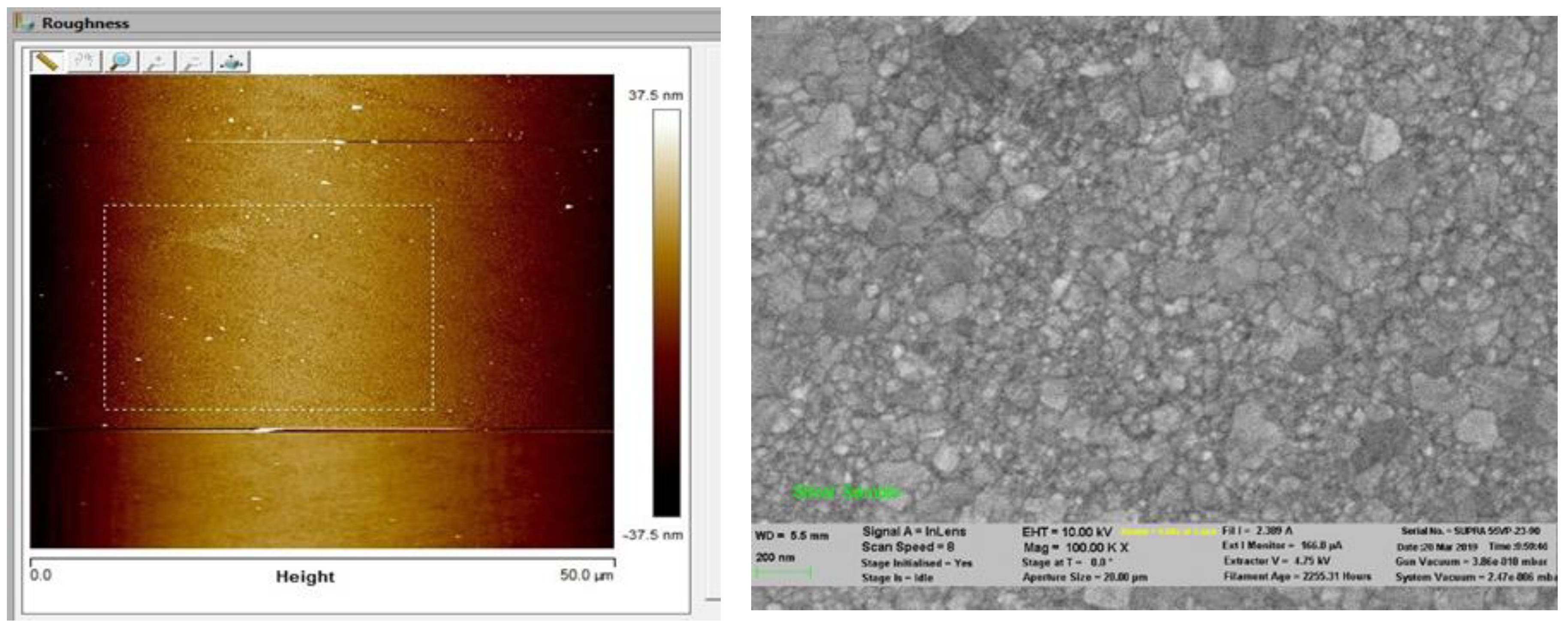
2. Experimental Details

Thin films of high-purity noble metals (purity ≥ 99.999%) were deposited over Quartz substrates in a class-100 clean room NanoFab. An AJA International thermal evaporator was used at a base pressure of 1 × 10⁻⁶ Torr with a deposition rate of about 1 Ǻ/s. The atomic force microscope (AFM) and scanning electron microscopies (SEM) were used to examine the surface topography and microstructure. Representative scans (AFM/SEM) of the Ag film are shown in Figure 1. The films are polycrystalline and densely packed with crystallites of sizes up to about a few hundred µm.
Figure 2 shows the schematic of our system used for simultaneous measurements of the surface plasmon resonance and electrical resistivity of the samples. Compared to the traditional Kretschmann configuration optical system [17,18,19,20], this system utilizes a recently developed fixed-detector Kretschmann configuration optical system for the SPR measurements. One of the advantages of the fixed-detector system is that it does not require the use of a ( θ , 2 θ ) goniometer [21]. The angular scans are accomplished by optically steering the incident laser beam. The λ = 632 nm radiation is obtained from a 1 mW He-Ne laser. It is partially reflected into the reference silicon detector. The output of the detector is amplified and recorded using a Data Studio module and LabView software. The magnitude of this reference signal is used to normalize the output of the other silicon detector produced by light reflected from the prism/sample used in the Kretschmann configuration. The laser beam transmitted through a partially reflecting plate is passed through a polarizer to obtain p-polarized light. The state of polarization is checked by the measurements of the Brewster’s angle. The incident angle at the sample for the polarized beam is adjusted by a rotating mirror. The reflected beam is steered by the rotation of the second mirror. The reflected beam is collected by second silicon detector, amplified, and recorded. Details of the procedure to determine the angle of incidence required for the surface plasmon resonance have been published elsewhere, and the basic equations are shown in Figure 3 [21].
For electrical resistivity measurements, a commercially available four-point probe assembly mounted on a precision micrometer was used. The Signatone probe (model SP4-40-045-TC-RS) uses Tungsten Carbide tips of 4 × 10⁻⁵ m radius, with 1.02 × 10⁻³ m spacing between the tips, and they exert a pressure equivalent to 4.5 × 10⁻² kg. The micrometer allows precise contact at four points of the thin-film sample. The outer two points are connected to a Keithley model 2400 Source Measure Unit (SMU), which is used as a current source. The inner two points are connected to a Keithley model 2182A Nanovolt meter. The current and voltage (IV data) readings are recorded in the computer using the LabView software. While conducting simultaneous measurements of the surface plasmon resonance and electrical resistivity, we obtained 100 IV curves for each angle of incidence. The IV curves were measured for three different ranges of currents: (1) low current range, from 100 nA to 1 μA; (2) mid current range, 1 μA to 10 μA; and (3) high current range, 10 μA to 100 μA. All three samples—(a) 43 nm-thick copper, (b) 50 nm-thick silver, and (c) 46 nm gold—show Ohmic behavior with the same resistivity at all three ranges of the currents.

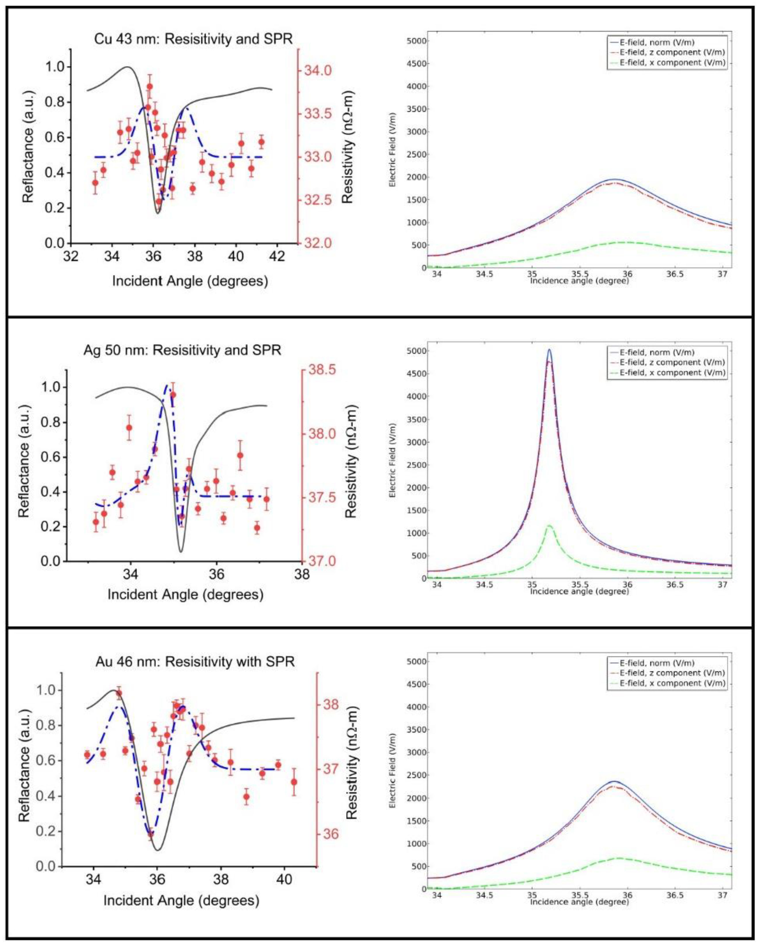
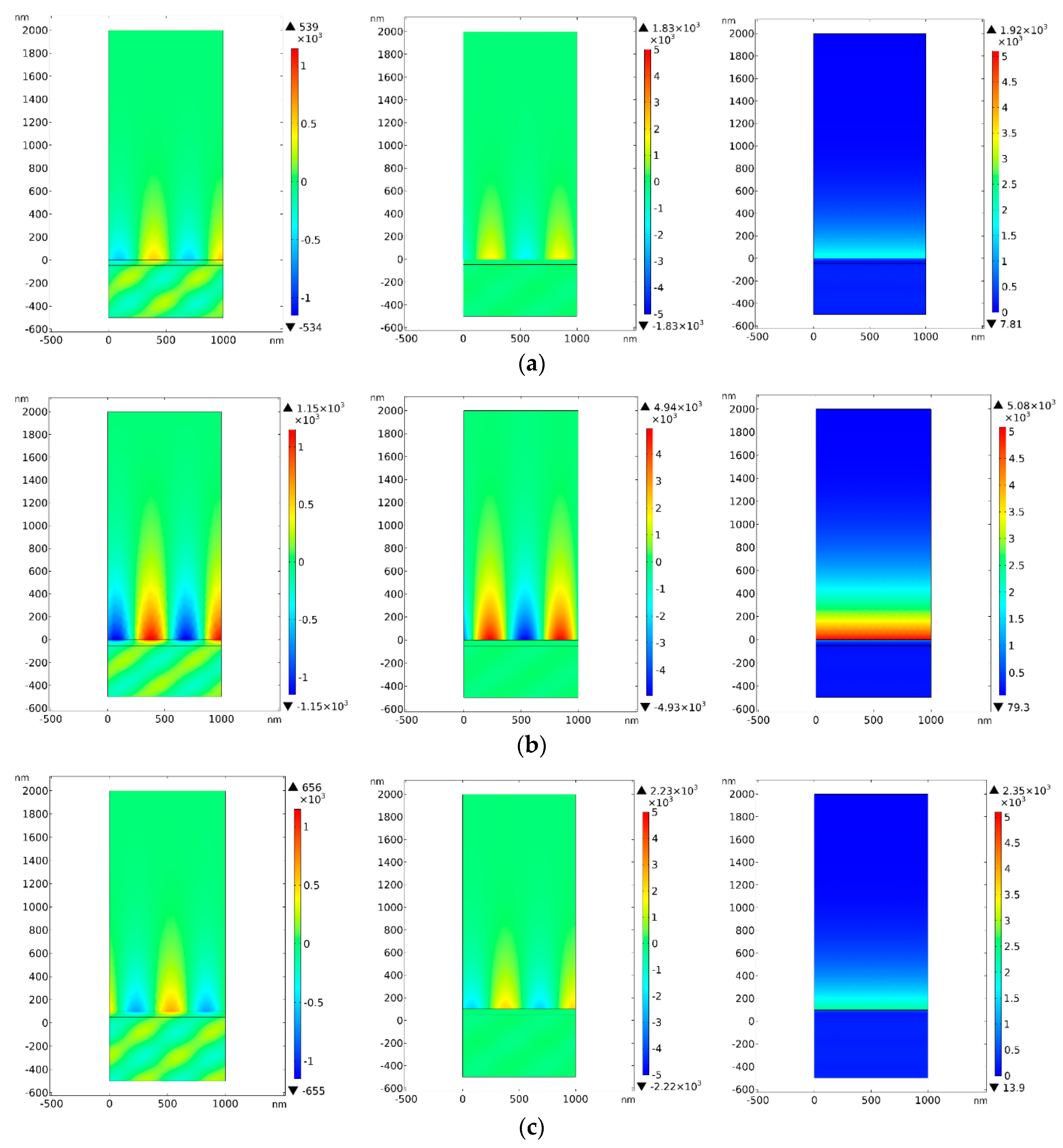
3. Results and Discussion

Figure 4 shows the surface plasmon resonance curves and electrical resistivity data for the Cu, Ag, and Au thin films. Specifically, the SPR data show the reflectivity of the p-polarized light as a function of the angle of incidence (angle ϕ in Figure 3) at the prism/sample assembly used in the Kretschmann optical system. The resonance occurs at incident angles around 35–36°. The incident angle at which resonance occur, is labelled as the resonance angles ( θ S P R ) . A tremendous loss in reflectivity is observed at the resonance angle because of the fact that the “missing energy” at this particular angle is used up to excite the surface plasmon polaritons. There is another angle of incidence that is important. It is the so-called critical angle ( θ c ) . For light passing from a medium of high refractive index to a medium of lower refractive index, it is the angle of incidence for which the angle of transmission is 90°. In the case of copper, for example, θ c ~ 35.5°. Between the critical angle and the resonance angle, the reflectivity changes from 100% at θ c down to almost zero at resonance in the case of the silver film. The overall quality of the SPR curve, the full width at half-maximum (FWHM), and the loss of reflectivity at θ S P R . reflect qualitatively the quality of the sample. We have observed in our previous works that (1) a high-quality sample produces a sharper SPR curve with an almost total loss of reflectivity at resonance and (2) the SPR curves are sensitive to the thickness of the sample [18,22,23,24]. The electrical resistivity data of the Cu, Ag, and Au films exhibit qualitatively similar behavior over the range of angles used in these measurements. In the case of the copper film, the resistivity increases from about 32.7 nΩ − m at 33.7° to a higher value of 33.6 nΩ − m at 35.7°. Thereafter, the resistivity decreases very significantly, and its angular dependence follows more or less the angular dependence of the SPR data. The electrical conductivity of the film reaches its highest value at resonance. It is noteworthy that the films become highly conducting at and around resonance. It is at resonance that the collective oscillations of the surface charges become most pronounced and the evanescent electric fields associated with the surface plasmon polaritons are the strongest. The rise of the conductivity to its highest value at resonance reflects the influence of the collective oscillations of the surface charges on the flow of the current through the top surface layers of the film. After resonance, the resistivity increases to about 33.5 nΩ − m at an angle which we label as θhigh–R ≤ 38°. For incident angles higher than θhigh–R, the resistivity decreases nonlinearly towards a value measured at higher angles.
It is striking that, within a range of angles around the resonance, the electrical resistivity mimics the shape of the surface plasmon resonance. The resistivities of the Ag and Au films too show a similar angular dependence. As stated above, the surface plasmons influence the electrical resistivity of the film through the evanescent electric fields. It is therefore important to examine the details of these electric fields present in each sample. Although we have not measured directly the evanescent electric fields, we observe their strength through changes in the resistivity of the material.
We have simulated the evanescent fields by using the finite difference method in COMSOL. We have published elsewhere details of the basic procedure used [25]. It requires mainly the wavelength of the light (632 nm) and the refractive indices of the material. In our simulations, the wavelength-dependent refractive indices of the films were obtained from the “refractive index data base” [26]. We used the following values: for Cu, ϵ1 = −11.542, ϵ2 = 1.8405; for Ag, ϵ1 = −18.281, ϵ2 = 0.48108; and for Au, ϵ1 = −11.740, ϵ2 = 1.2611. The results for the evanescent fields, the components along the surface, the components vertical to the surface, and the resultant field are shown in Figure 5.
The normal to the surface components are approximately 1.8, 4.9, and 2.2 kV/m for copper, silver, and gold films, respectively. The components along the surface are approximately 0.5, 1.2, and 0.6 kV/m. The resultant electric fields are approximately 1.9, 5, and 2.3 kV/m for copper, silver, and gold, respectively. The decay lengths for the normal-to-the surface components are of the order of 300–400 nm. It is clear from the data presented in Figure 4 that the electrical conductivity of the noble metal thin films is enhanced very significantly within a range of angles around the resonance. Since it is the collective oscillations of the surface charges that are responsible for the resonance, the same oscillations should also be responsible for the observed enhancement in the electrical conductivity of the film.

4. Conclusions

In conclusion, we have presented evidence that surface plasmon resonance can significantly influence the flow of electrons through the surface layers of noble metal thin films. To our knowledge, these are the first experimental data which support the theoretical models proposed by Bohm, Pines, Frohlich, and Garland in the 1950s–1960s [12,13,14,15,16,25,26,27], whereby the Umklapp electron–electron scattering and attractive interactions between free electrons due to the screening of the d-band electrons by the s-band electrons can enhance electrical conduction in 2D transition metals. The COMSOL simulations of the evanescent electric fields of the surface plasmons support the experimental data on the changes in the resistivity at and around resonance. The results are important to the advancements of the electronic devices in which the flow of the electrons can be controlled by the evanescent electric fields of the surface plasmons. The strength of such fields can be controlled by a variety of techniques—for example, by adjusting the distance between the device and the SPR generating “module” (high-index prism/metal), and/or by changing the angle of incidence of the polarized beam that produces SPR at the module. It is believed that the data presented here will stimulate additional experimental as well as theoretical advances in the field.

Author Contributions

Conceptualization, S.C.S.; Data curation, V.K., H.A. and N.H.; Formal analysis, V.K. and H.A.; Investigation, S.C.S.; Project administration, S.C.S.; Software, D.Z.; Supervision, S.C.S.; Writing–original draft, S.C.S.; Writing–review & editing, S.C.S. All authors have read and agreed to the published version of the manuscript.

Funding

This research received no external funding

Conflicts of Interest

The authors declare no conflict of interest.

References

  1. Raether, H. Surface Plasmons on Smooth and Rough Surfaces and on Gratings; Springer: Berlin/Heidelberg, Germany, 1988. [Google Scholar]
  2. Novotny, L.; Hecht, B. Principles of Nano-Optics, 2nd ed.; Cambridge University Press: Cambridge, UK, 2012. [Google Scholar]
  3. Pitarke, J.M.; Silkin, V.M.; Chulkov, E.V.; Echenique, P.M. Theory of surface plasmons and surface-plasmon polaritons. Rep. Prog. Phys. 2007, 70, 1–87. [Google Scholar] [CrossRef]
  4. Zayats, A.V.; Smolyaninov, I.I.; Maradudin, A.A. Nano-optics of surface plasmon polaritons. Phys. Rep. 2005, 408, 131–314. [Google Scholar] [CrossRef]
  5. Zayats, A.V.; Smolyaninov, I.I. Near-field photonics: Surface plasmon polaritons and localized surface plasmons. J. Opt. A Pure Appl. Opt. 2003, 5, S16–S50. [Google Scholar] [CrossRef]
  6. Sharma, S.C. Surface Plasmon Resonance Sensors: Fundamental Concepts, Selected Techniques, Materials, and Applications. In Advances in Sensors: Reviews’ Book Series; Yurish, S.Y., Ed.; IFSA Publishing: Barcelona, Spain, 2018; Volume 5, pp. 25–77. [Google Scholar]
  7. Ritchie, R.H. Plasma Losses by Fast Electrons in Thin Films. Phys. Rev. 1957, 106, 874–881. [Google Scholar] [CrossRef]
  8. Kittel, C. Introduction to Solid State Physics, 7th ed.; Wiley: Hoboken, NJ, USA, 1996. [Google Scholar]
  9. Homola, J.; Koudela, I.; Yee, S.S. Surface plasmon resonance sensors based on diffraction gratings and prism couplers: Sensitivity comparison. Sens. Actuators B Chem. 1999, 54, 16–24. [Google Scholar] [CrossRef]
  10. Kneipp, K.; Flemming, J. Surface Enhanced Raman-Scattering (Sers) of Nucleic-Acids Adsorbed on Colloidal Silver Particles. J. Mol. Struct 1986, 145, 173–179. [Google Scholar] [CrossRef]
  11. Pines, D. Electron Interaction in Solids. Can. J. Phys. 1956, 34, 1379–1394. [Google Scholar] [CrossRef]
  12. Bohm, D.; Pines, D. Screening of Electronic Interactions in a Metal. Phys. Rev. 1950, 80, 903–904. [Google Scholar] [CrossRef]
  13. Pines, D.; Bohm, D. A Collective Description of Electron Interactions. Collective Vs Individual Particle Aspects of the Interactions. Phys. Rev. 1952, 85, 338–353. [Google Scholar] [CrossRef]
  14. Bohm, D.; Pines, D. A Collective Description of Electron Interactions. Coulomb Interactions in a Degenerate Electron Gas. Phys. Rev. 1953, 92, 609–625. [Google Scholar] [CrossRef] [Green Version]
  15. Garland, J.W. Mechanisms for Superconductivity in Transition Metals. Phys. Rev. Lett. 1963, 11, 111. [Google Scholar] [CrossRef]
  16. Frohlich, H. Superconductivity in Metals with Incomplete Inner Shells. J. Phys. Part C Solid 1968, 1, 544. [Google Scholar] [CrossRef]
  17. Tiwari, K.; Sharma, S. C. plasmon based sensor with order-of-magnitude higher sensitivity to electric field induced changes in dielectric environment at metal/nematic liquid-crystal unterface. Sens. Actuators A Phys. 2014, 216, 128–135. [Google Scholar] [CrossRef]
  18. Tiwari, K.; Sharma, S.C.; Hozhabri, N. High performance surface plasmon sensors: Simulations and measurements. J. Appl. Phys. 2015, 118, 093105. [Google Scholar] [CrossRef]
  19. Tiwari, K.; Sharma, S.C.; Hozhabri, N. Hafnium dioxide as a dielectric for highly-sensitive waveguide-coupled surface plasmon resonance sensors. AIP Adv. 2016, 6, 045217. [Google Scholar] [CrossRef] [Green Version]
  20. Tiwari, K.; Singh, A.; Sharma, S.C. Evidence for surface plasmons in a liquid crystal containing gold nanoparticles. Appl. Phys. Lett. 2012, 101. [Google Scholar] [CrossRef]
  21. Singh, A.K.; Sharma, S.C. A fixed detector Kretschmann configuration optical system to study surface plasmon excitations. Opt. Laser Technol. 2014, 56, 256–262. [Google Scholar] [CrossRef]
  22. Tiwari, K. Bimetallic Waveguide-Coupled Sensors for Tunable Plasmonic Devices. Ph. D. Thesis, University of Texas at Arlington, Arlington, TX, USA, 2015. [Google Scholar]
  23. Akafzade, H. Theoretical and Experimental Probes of Dispersion in Two-Dimensional Materials. Ph.D. Thesis, University of Texas at Arlington, Arlington, TX, USA, 2020. [Google Scholar]
  24. Hussein, A.; Sharma, S.C. New Metamaterial as a Broadband Absorber of Sunlight with Extremely High Absorption Efficiency. AIP Adv. 2020, 10, 035209. [Google Scholar] [CrossRef] [Green Version]
  25. Bohm, D.; Huang, K.; Pines, D. Role of Subsidiary Conditions in the Collective Description of Electron Interactions. Phys. Rev. 1957, 107, 71–80. [Google Scholar] [CrossRef]
  26. Bohm, D.; Pines, D. A Collective Description of Electron Interactions. Magnetic Interactions. Phys. Rev. 1951, 82, 625–634. [Google Scholar] [CrossRef]
  27. Fröhlich, H. Theory of Dielectrics; Dielectric Constant and Dielectric Loss, 2nd ed.; Clarendon Press: Oxford, UK, 1958; p. 192. [Google Scholar]
Figure 1. AFM and SEM scans of the silver thin film.
Condensedmatter 05 00052 g001
Figure 2. Block diagram of the experimental set-up for simultaneous measurements of the surface plasmon resonance and electrical resistivity of the thin-film samples.
Condensedmatter 05 00052 g002
Figure 3. Calculation of the angle of incidence ( ϕ ) at the base of the prism used in the optical system. The polarized laser travels horizontally to M1.
Condensedmatter 05 00052 g003
Figure 4. SPR and resistivity data: top row for copper, middle row for Ag, and bottom row for Au. In the first panel of each row, the solid curve represents SPR and the broken dashed curve is drawn through the resistivity data to aid the eyes. The second panel in each row shows COMSOL simulations for the evanescent electric field of the SPR.
Condensedmatter 05 00052 g004
Figure 5. COMSOL simulations of the evanescent electric fields in the noble metal thin films. The results for the Cu (a), Ag (b), and Au (c) films are shown in the top, middle, and bottom rows, respectively. In each row, the panels from left to right show electric field components along the surface, normal to the surface, and resultant.
Condensedmatter 05 00052 g005

