1. Introduction
In modern studies carried out in biology, chemistry and medicine, it is often necessary to measure the refractive index of liquid solutions [
1,
2], and the refractive index of these solutions may change under the influence of certain factors, (e.g., during the chemical reactions in solution). Therefore, the change in the refractive index must be measured quickly, usually in real time. It should also be noted that the volume of the analyzed medium is often quite small. For these purposes, a number of sensing elements included in the sensors have been proposed, which are based on the occurrence of various resonance phenomena in the optical range. This is the resonance of the surface plasmon–polariton waves in the Otto–Kretschmann scheme [
3,
4,
5,
6], resonance of the surface plasmon–polariton waves in periodic structures [
7,
8] and waveguide resonance in dielectric grating on a metal substrate [
9,
10]. The operation of the sensors is based on the change in the resonant wavelength at a fixed incidence angle of the test beam or in a change in a resonant angle on a fixed wavelength when the refractive index of the analyzed medium is changing. Periodic structures, in which various types of resonance are present, are also studied, which leads to interesting effects. In particular, dielectric metamaterials have high-quality resonances, which are affected by laser radiation, which leads to their spectral shift [
11], and created a new family of nanodevices on the basis of plasmonic metasurfaces based on metal oxides [
12], which may be another step towards the creation of optical computers. Metasurfaces can have unexpected properties (e.g., an artificial nanomechanical metasurface, formed by a subwavelength nanowire array that changes color during mechanical deformation), which can be the basis for creating multifunctional photon filters, switches and voltage sensors [
13]. Additionally, in [
14] it is shown that strong near-flat absorption in a wavelength range from visible to near-infrared (wider than in plasmonic metal metasurfaces) can be provided by free-standing diamond membrane, structured by focused ion beam milling. We see that periodic structures show unexpected effects, which can lead to the creation of a new type of optical devices.
Consider the following idea of measuring the refractive index change of the analyzed medium. These measurements are based on the change in the resonant wavelength due to the change in the refractive index. Sensitivity in this method can be defined as , as well as the resonant curve half-width , where —slight change of the refractive index of analyzed medium, —resonant wavelength change, due to the change of the refractive index of analyzed medium by . The system will be more sensitive to the refractive index change, as is higher, and with as low as possible.
Sensors, based on the resonance of plasmon–polariton waves in gratings (either dielectric or metal) on a metal substrate (gold or silver) has very narrow spectral band (around 1 nm near wavelength 1
), and also, they have quite large value of
that can be assessed by:
where
—grating period,
—dielectric permittivity of the analyzed medium,
dielectric permittivity of the metal substrate. This equation determines the conditions of the surface plasmon–polariton resonance for the normal incidence of light beam.
In these structures there is a great electric field at resonance in the grating layer. If we have dielectric grating, the electric field will occupy quite a large volume, with a resonant thickness of the grating 13–120
[
15] for a grating period 1
. That is why such structures should have very good accuracy, which is confirmed by theoretical analysis. Theoretical analysis can be performed by RCWA or finite-element methods, with periodical grating. However, diffraction grating with strict periodicity cannot be manufactured, because grating lines (or bars) will not be uniform. This leads to the increase in the spectral width of the resonant peak, and to the decrease in its amplitude. Such a conclusion can be made through analysis [
9], where it is experimentally confirmed that the resonant peak becomes lower and significantly wider compared to the theoretical calculations; however, resonant wavelengths in both cases match.
In order to obtain waveguide effects in a structure, a layer with a refractive index higher than the refractive index of the substrate and analyzed medium is required. For this purpose, in [
9,
10] a thick film with higher refractive index was applied. After that, relief grating was formed on photoresist applied on this film. As a result, we obtained a layer with the highest average refractive index, formed by two layers: homogeneous and relief grating layer, where its cavities are filled with analyzed medium. At the waveguide resonance, strong electric field arise in those layers. However, in this case, the volume of the field interaction with analyzed medium is very low, leading to low sensitivity. In [
16], dielectric grating was formed on a photoresist layer applied directly on a substrate. In this case, at the waveguide resonance, the interaction volume was significantly higher and, as a result, the sensitivity of the refractive index change measurement was much higher.
We can conclude that sensitivity will be much higher, the higher the volume of the strong electric field interaction with an analyzed medium. Additionally, an average refraction index of grating layer should be higher than the refractive index of analyzed medium and substrate.
2. Numerical Analysis of the Waveguide Resonance in Phase Grating
Figure 1 shows the investigated periodic structures, which are a three-dimensional dielectric grating deposited on a dielectric substrate, as shown in
Figure 1a, and a metal or dielectric grating formed on a metal substrate, as shown in
Figure 1b. In both cases, the grating interacts with the test medium. At the waveguide resonance, a strong field appears in the dielectric grating, which can exceed the amplitude of the incident wave by two orders, and the reflection coefficient will be equal to one [
17]. When the resonant excitation of the surface plasmon–polariton wave in a periodic structure with a metal substrate occurs due to absorption in the metal, the reflection coefficient can be equal to zero. When the refractive index of the analyzed medium changes, the resonance is disturbed and occurs at a different wavelength at a constant incidence angle of the beam, which is the basis of sensors of this type.
In order for waveguide resonance to occur in the phase grating, the average refractive index of the grating medium must be greater than the refractive index of the substrate medium and test medium . This requirement arises from the condition of the waveguide effect occurrence and from the existence condition of a waveguide mode with a discrete constant propagation The sensitivity will be greater if the field in the test environment is large enough. In order to obtain high sensitivity in our waveguide structure, the refractive index of the substrate should be as low as possible. As the substrate, you can use the plate of fused quartz, the refractive index of which is approximately equal to 1.45 in the red region of the spectrum.
Figure 2 shows the distribution of the square modulus of the electric field amplitude for the waveguide mode at a wavelength of 740 nm.
According to
Figure 2, the field is the largest in the testing region with the presence of a buffer layer with a low refractive index, and the blue and green points lie well on the red curve. That is, the refractive index of the substrate does not significantly affect the distribution of the field in the structure with the presence of a buffer layer of a thickness 1 μm. It should be noted that the “stabilizing” effect of the buffer layer will decrease as its thickness decreases. However, even at a thickness of this layer 0.35 μm, shown by
x = 1 μm in
Figure 2, the field at the boundary of the buffer layer/substrate is almost zero.
If a substrate with a refractive index of 1.45 is present without a buffer layer, then the field distribution is slightly worse than the corresponding distribution in the presence of a buffer layer with a refractive index of 1.38. It should also be noted that in the presence of a buffer layer, the maximum of the field is concentrated in the grating at . If the refractive index of the substrate is 1.515, then the maximum of the field is concentrated at (green curve) (i.e., such a structure will have low sensitivity).
When the guided-mode resonance is excited in the grating structure, the following equation is satisfied:
Sensitivities of the propagation constant at resonance to the change of the wavelength and refractive index of analyzed medium change we can calculate using:
Based on these sensitivities, we can determine the spectral and angular sensitivity to the change in the refractive index of analyzed medium. Sensitivity of the resonant wavelength change due to the change of the investigating solution refractive index can be described as:
And sensitivity of the resonant angle change is expressed as:
where
We can see that, with increasing incident angle and wavelength, sensitivity increases.
Table 1 shows the resonant wavelengths for some angles and the sensitivity
,
,
,
for the following waveguide structure parameters:
,
According to
Table 1, the sensitivity
S increases with increasing incidence angle of the test beam due to the increase in
Sn and increase in
Sλ (decrease in modulus), and
Sλ has a greater influence on the sensitivity
S than
Sn. It can be noted that the resonant wavelength changes significantly with increasing incidence angle on the sensitive structure.
The following
Table 2 shows the resonant wavelengths and sensitivities
,
,
,
depending on the refractive index n
a of the test medium at the incidence angle of the light beam 30° in the presence of a buffer layer with a refractive index of 1.38. If there is no buffer layer, the data are given in the denominator of the cells in the table. Other parameters are:
,
Analyzing
Table 2, we can conclude that the sensitivities in the presence of a buffer layer with a low refractive index increase by at least three times compared to the sensitivities in the absence of a buffer layer. In addition, it can be noted that the sensitivity increases sharply as the refractive index of the test medium increases, especially when approaching
to
The resonant wavelengths do not change significantly as
changes from 1 to 1.5.
3. Numerical Analysis of Surface Plasmon–Polariton Resonance by Grating on Metallic Substrate
Resonance absorption of the electromagnetic wave energy is observed at carefully selected parameters of the grating and wavelength. The grating parameters and the resonant wavelengths are given in
Table 2 for a silver substrate.
In
Table 2,
—resonant thickness of the grating,
—Fill-factor,
—dielectric permittivity of the grating part, with width
Dielectric permittivity of silver was calculated based on the analytical formula provided in [
18]. These analytical formulas approximate the spectral dependences of the dielectric permittivity in the interval 0.3–2.0 µm and are obtained on the basis of experimental data presented in [
19,
20].
Comparison of columns 5 and 6 shows a good fitting of the resonant wavelengths determined by two methods. The angle of incidence of the optical wave on the grating is normal in all calculations. The grating period is 1 μm for all examples.
Figure 3 shows the spectral dependence of the reflection coefficient for the structure number 3. The width of the resonance curve is equal to 0.8 nm, that is, the
—factor is equal to
. The resonance will be disturbed when the refractive index of the environment changes at such a high
—factor Therefore, such structures can be used as sensitive sensor elements.
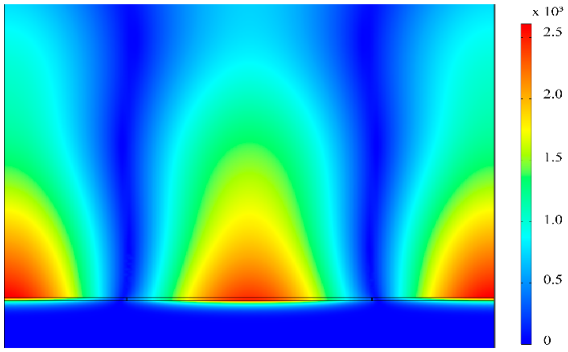
The distribution of the electric field above the grating for the periodic structure No. 3 is shown in
Figure 4. It can be seen that the strongest field is concentrated in a rather small volume.
Figure 5 shows the distribution of the magnetic field above the grating. It should be noted that the strongest field occupies a significant volume above the grating.
It is known that gold is more resistant to external influences, and its characteristics from the point of view of the resonance of plasmon–polariton waves are slightly worse than silver.
Table 3 shows the parameters of the SPP resonance for the gold substrate. The comparison of columns 6 and 7 show a good fitting of the resonance wavelengths determined by two methods. The angle of incidence of the optical wave on the grating is normal in all calculations. In addition, the width of the resonances for the gold substrate is greater than for the silver substrate. This is due to the fact that the imaginary part of gold dielectric permittivity is higher than the imaginary part of the silver permittivity.
There are the strong electric and magnetic fields with amplitudes that are much larger than the incident wave amplitude at resonance in the grating. The strong magnetic field occurs at resonance in structures Nos. 1 and 3 with the silver substrate, which is significant in the grating period. It is obvious that such structures can be used to study the luminescence of substances caused by the magnetic dipole interaction.
The strong electric field is concentrated in a small volume near the vertices of a rectangular cross section in structures Nos. 1, 2, and 3 (metal gratings). Therefore, the strong field will come in contact with the test substance in a small volume. The strong magnetic field is concentrated in the dielectric for the dielectric grating (Nos. 4, 5 and 6). Thus, this field will not contact with the researched substance. However, there is a strong electric field in these structures, which occupies a large volume above the grating, especially for structure No. 5. It is obvious that such structures with SPP resonance are expedient to be used for Raman spectroscopy and the study of the luminescence excited during electrical dipole interaction. The strong electric field is concentrated in the small volume near the vertices of the rectangular cross section in structure No. 1 (gold grating on a gold substrate).
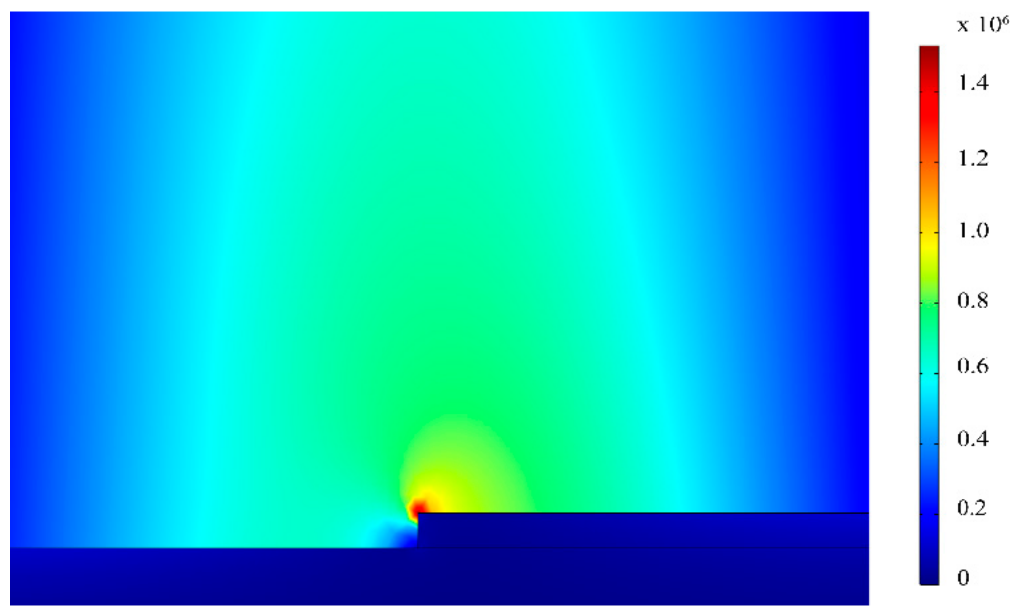
The distribution of the electric field in the periodic structure at the resonant wavelength is shown in
Figure 6. It can be seen that the strongest field is concentrated in a fairly small volume. Therefore, the strong field will come in contact with the test substance in a small volume. However, the magnetic field takes up a significant volume above the grating and will strongly interact with the test substance.
Figure 7 shows the distribution of the magnetic field in the grating on gold substrate. The enhanced field occupies a considerable volume above the grating.
Thus, it is appropriate to use such a structure to study luminescence excited by magnetic–dipole interaction. The strong magnetic field is concentrated in the dielectric for the dielectric grating (Nos. 2 and 3) on the gold substrate and this field will not contact with test the substance. However, there is a strong electric field in these structures, which occupies a large volume above the grating. It is obvious that such structures under plasmon–polariton resonance are expediently used for Raman spectroscopy and the study of luminescence excited during electrical dipole interaction. Structure No. 3 can be used to study the aqueous solutions of active substances, because the wavelength of the resonance is determined by the refractive index of the solution.
Figure 8 shows the change in the wavelength of the resonance for the structure No. 2, as shown in
Figure 8a, and No. 3, as shown in
Figure 8b, from
Table 2.
It can be concluded from
Figure 8 that there is the strong linear dependence of the change in the resonant wavelength on the change in the refractive index.
The sensitivity for structure No. 2 is 0.91 microns (gas), and for structure No. 3 (aqueous solutions) the sensitivity is equal to 0.67 microns. The change in the resonant wavelength is proportional to the change in the refractive index of the medium.
Thus, such periodic structures can be used as sensing elements for sensors to measure the refractive indexes of aqueous or other solutions exposed to various chemical reagents.
There are the strong magnetic fields in structures 1 and 3 with a silver substrate at the resonance if the field occupies a considerable volume on the grating period. Such structures can be used to study the luminescence of substances caused by magnetic dipole interaction. In structure No. 1 (gold grating on the gold substrate), the strong electric field is concentrated in a small volume near the vertices of a rectangular cross section. Therefore, a strong field will come in contact with the test substance in a small volume. However, the magnetic field occupies a significant volume above the grating and will strongly interact with the test substance. Therefore, it is appropriate to use such a structure to study luminescence excited by magnetic–dipole interaction under surface plasmon–polariton resonance conditions.


