Article

Effect and Characterization of Stone–Wales Defects on Graphene Quantum Dot: A First-Principles Study

by
Gargi Chakraborti (Banerjee)
1,
Arka Bandyopadhyay
2 and
Debnarayan Jana
2,*
1
Department of Physics, St. Thomas’ College of Engineering Technology, 4, Diamond Harbour Road, Kidderpore, Kolkata 700023, India
2
Department of Physics, University of Calcutta, 92 Acharya Prafulla Chandra Road, Kolkata 700009, India
*
Author to whom correspondence should be addressed.
Condens. Matter 2018, 3(4), 50; https://doi.org/10.3390/condmat3040050
Submission received: 14 November 2018 / Revised: 7 December 2018 / Accepted: 12 December 2018 / Published: 17 December 2018

Abstract

:
A first principles based density functional theory (DFT) has been employed to identify the signature of Stone–Wales (SW) defects in semiconducting graphene quantum dot (GQD). Results show that the G mode in the Raman spectra of GQD has been red shifted to 1544.21 cm 1 in the presence of 2.08% SW defect concentration. In addition, the intensity ratio between a robust low intense contraction–elongation mode and G mode is found to be reduced for the defected structure. We have also observed a Raman mode at 1674.04 cm 1 due to the solo contribution of the defected bond. The increase in defect concentration, however, reduces the stability of the structures. As a consequence, the systems undergo structural buckling due to the presence of SW defect generated additional stresses. We have further explored that the 1615.45 cm 1 Raman mode and 1619.29 cm 1 infra-red mode are due to the collective stretching of two distinct SW defects separated at a distance 7.98 Å. Therefore, this is the smallest separation between the SW defects for their distinct existence. The pristine structure possesses maximum electrical conductivity and the same reduces to 0.37 times for 2.08% SW defect. On the other hand, the work function is reduced in the presence of defects except for the structure with SW defects separated at 7.98 Å. All these results will serve as an important reference to facilitate the potential applications of GQD based nano-devices with inherent topological SW defects.

1. Introduction

The successful experimental fabrication of the two dimensional (2D) nanostructure graphene was a path breaking event in the field of material science. The pure graphene sheet exhibits several unique optical, electronic and mechanical properties [1,2]. However, the implementation of pure graphene in the opto-electronic industry is restricted by its zero band gap nature. Various efforts have been made to tune the Dirac-like dispersion relation by means of external perturbations [3,4,5,6,7]. It is well established that electronic and optical properties are interdependent. Therefore, the modulation of band structure can also be realized from the optical responses [8] for different graphene like systems [9]. Another favorable approach in band gap engineering is to reduce the dimension of graphene by proper structural tailoring [10,11,12,13]. Graphene quantum dots (GQDs) are very small fragments of graphene, where the motion of electrons is confined in three spatial directions. The properties of these GQDs are very much different from that of graphene. The underlying reasons for such difference are generally localization of electrons because of the quantum confinement effect and the existence of edge states. The GQDs are generally semiconducting in nature and the band gap can be tuned by varying the shape, size and surface chemistry [14,15,16]. Because of these tunable band gaps, GQDs can be used in photovoltaic devices [17,18]. Clearly, a graphene sheet does not allow photovoltaic applications because of the zero band gap nature. In addition, GQDs have also been observed to facilitate potential applications in organic LEDs [19], fuel cells [20], bio-imaging [21,22], bio-sensing [23,24], and environmental monitoring devices [25].
Point defects in graphene have drawn enormous interest because of their unavoidable existence in sample preparation [26,27,28,29,30]. The Stone–Wales (SW) defect [31,32] is a customary topological disorder in the graphene systems and its derivatives i.e., carbon nanotubes [33], nanoribbons [34] and fullerenes [35]. This involves rotation of carbon-carbon (C-C) bonds with respect to the midpoint by an angle π / 2 . As a result, four neighbouring hexagons are transformed into two heptagon-pentagon (7-5) pairs. These types of defects can also be artificially engineered in the laboratory [36]. The specific position of the defects can be identified with the help of transmission electron microscope (TEM) [36,37]. It is evident from previous reports that concentration as well as the specific positions of the defects crucially determine the hybridization and stability of the systems. These modifications have immense impact on the electronic band structure [38], and, hence, on the conductivity of the system [39,40]. In this context, it is worth mentioning that Lu et al. [41] have successfully transformed C 60 molecules into equal sized graphene quantum dots. Although SW defects are extremely common in the fullerene molecules [35], the effects of SW defects on graphene quantum dots have been less explored.
Raman spectroscopy [42] is a widely used non-invasive characterization technique for the carbon networks. The nature and concentration of defects on graphene like systems can be efficiently identified using this tool [43,44,45,46]. For example, the first order Raman spectrum of graphene exhibits single predominant stretching like mode called G band [42]. This mode is a signature of s p 2 hybridized C atoms in the system. The other defect related bands (D band) are due to second order Raman scattering process and it does not have any impact on the first order vibrational spectra. In addition, infra-red (IR) spectroscopy is another efficient tool for the characterization of carbon bonded materials. One can easily comment on the vibrational states of any system by studying the variation of IR frequencies of the incident electromagnetic radiation.
Motivated by the above discussions, we have systematically investigated the effect of SW defects on the vibrational and electronic properties of the graphene quantum dot (GQD). The effects have been explored for different concentrations and different positions of the SW defects. This paper has been organized as follows. First, the computational methodologies have been presented. In the next section, we have critically commented on the structural modifications due to the presence of SW defects in the system. Afterwards, we have extensively discussed the impact on the Raman and IR spectra of the GQD, followed by the variation in electronic properties i.e., dipole moment variation, effect on conductivity, work function, energy gap, etc. Finally, conclusions are drawn in Section 7. We expect that these results will broaden the possibilities of GQDs to be used in nano-electronic devices.

2. Computational Details

All the calculations have been performed under the framework of density functional theory (DFT) as implemented in the software Gaussian 09W [47]. The self-consistent ground state (true minima) has been achieved using Becke three parameters functional with Lee–Yang–Parr non-local electron correlation (B3LYP) [48,49] and the basis set 6-31G(d). We have used the optimized geometry for vibrational analysis with the same functional and basis set. The Hessian matrix (f) contains the second order partial derivatives of the potential ( Φ ) with respect to atomic displacements (x) from equilibrium positions as described in Equation (1)
f p , q = 2 Φ x p x q e q u i l i b r i u m .
Order of the matrix depends on the number of atoms (N) in the system. These force constants are further rewritten in terms of mass (m) weighted Cartesian coordinates ( f m w c ) as shown in Equation (2)
f m w c ; p , q = 2 Φ X p X q e q u i l i b r i u m .
Here, X p = m p x p and X q = m q x q . The square roots of the eigenvalues of the above 3 N × 3 N matrix give rise to the fundamental frequencies of the system. The translational and rotational modes are then separated out and Schmidt orthogonalization gives rise to the remaining 3 N–6 N vibrational modes. All these frequencies are verified to be real for the stability purpose. Raman intensities ( I i ) have been calculated from the Raman scattering activity ( S i ) for the i-th normal mode using Equation (3)
I i = f ( ν 0 ¯ ν i ¯ ) 4 S i ν i ¯ e h c ν i ¯ k T .
Here, ν 0 ¯ is the wavenumber (WN) of the incident photon, ν i ¯ is the WN of i-th normal mode, h is the Planck’s constant, c is the speed of light, k is Boltzmann constant and f is the normalization factor. This calculation has been performed at temperature 293.15 K and an exciting wavelength 785 nm. The Raman and IR spectra are plotted with Lorentzian envelope with full width half maximum (FWHM) equal to 5 cm 1 for better understanding. Besides, a scaling factor 0.9614 has been employed to obtain the actual WN from the DFT generated data in accordance with our basis/functional pair [50].
It is worth noting that the electronic ground state of the systems gets perturbed due to the first order Raman scattering process. However, the electronic state returns to the same ground state with different vibrational level after each event. Therefore, we have also explored the density of states (DOS) of the systems with the help of GaussSum 3.0 software [51]. HOMO and LUMO are the highest occupied molecular orbital and lowest unoccupied molecular orbital of the systems and the difference between their energies (E L U M O − E H O M O ) is essentially the band gap of the systems. We have additionally calculated the activation energy or work function of the systems from the difference between energies of the vacuum level and the HOMO (W = E v a c u u m − E H O M O ).

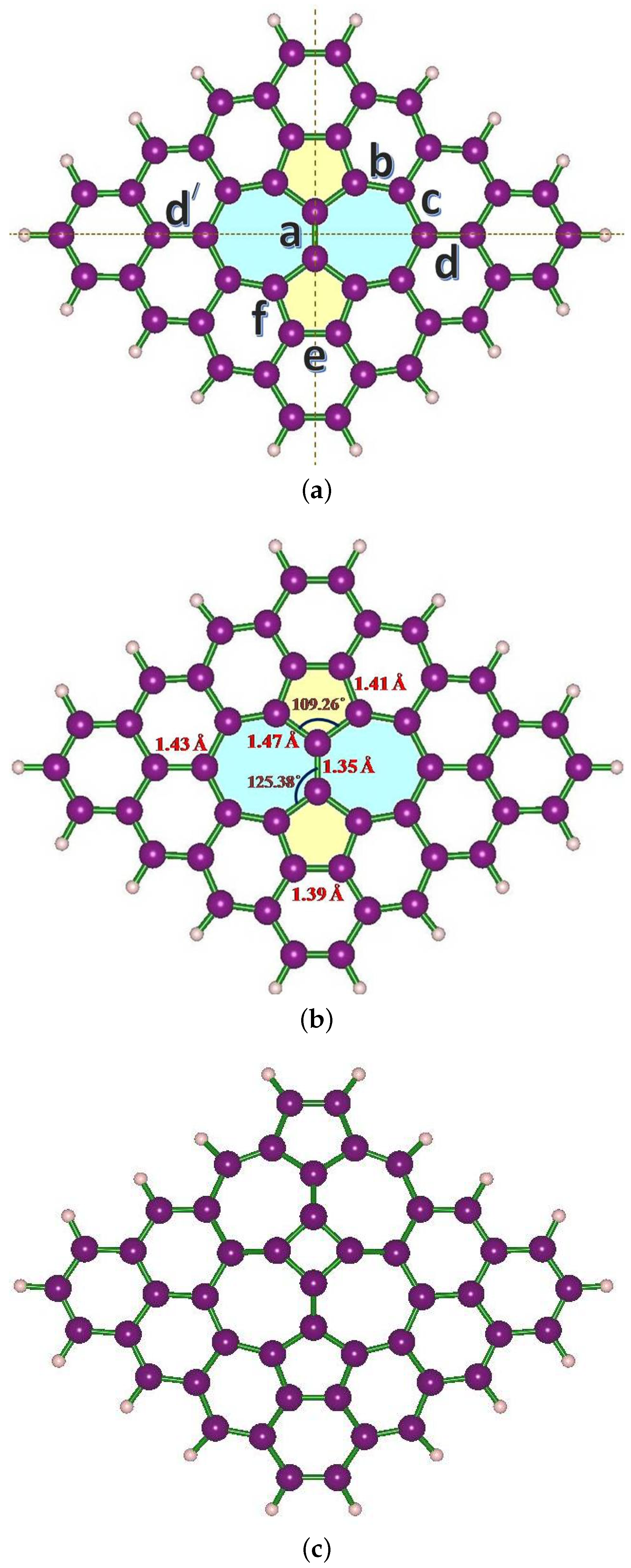
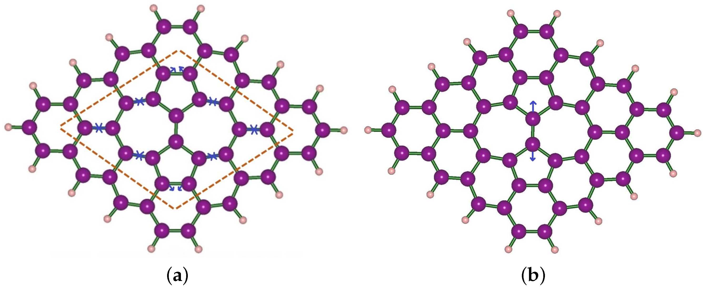
3. Structural Modifications
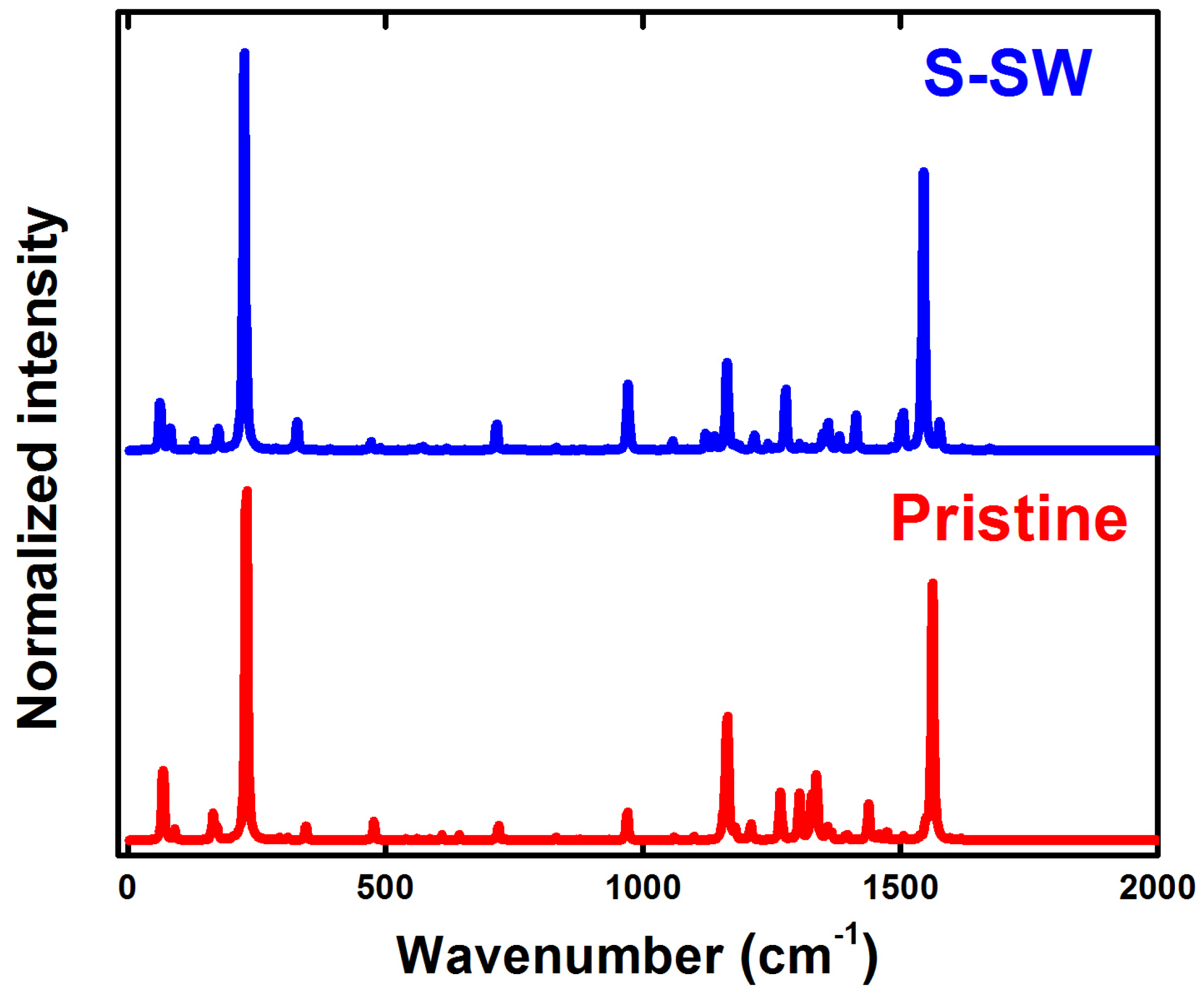
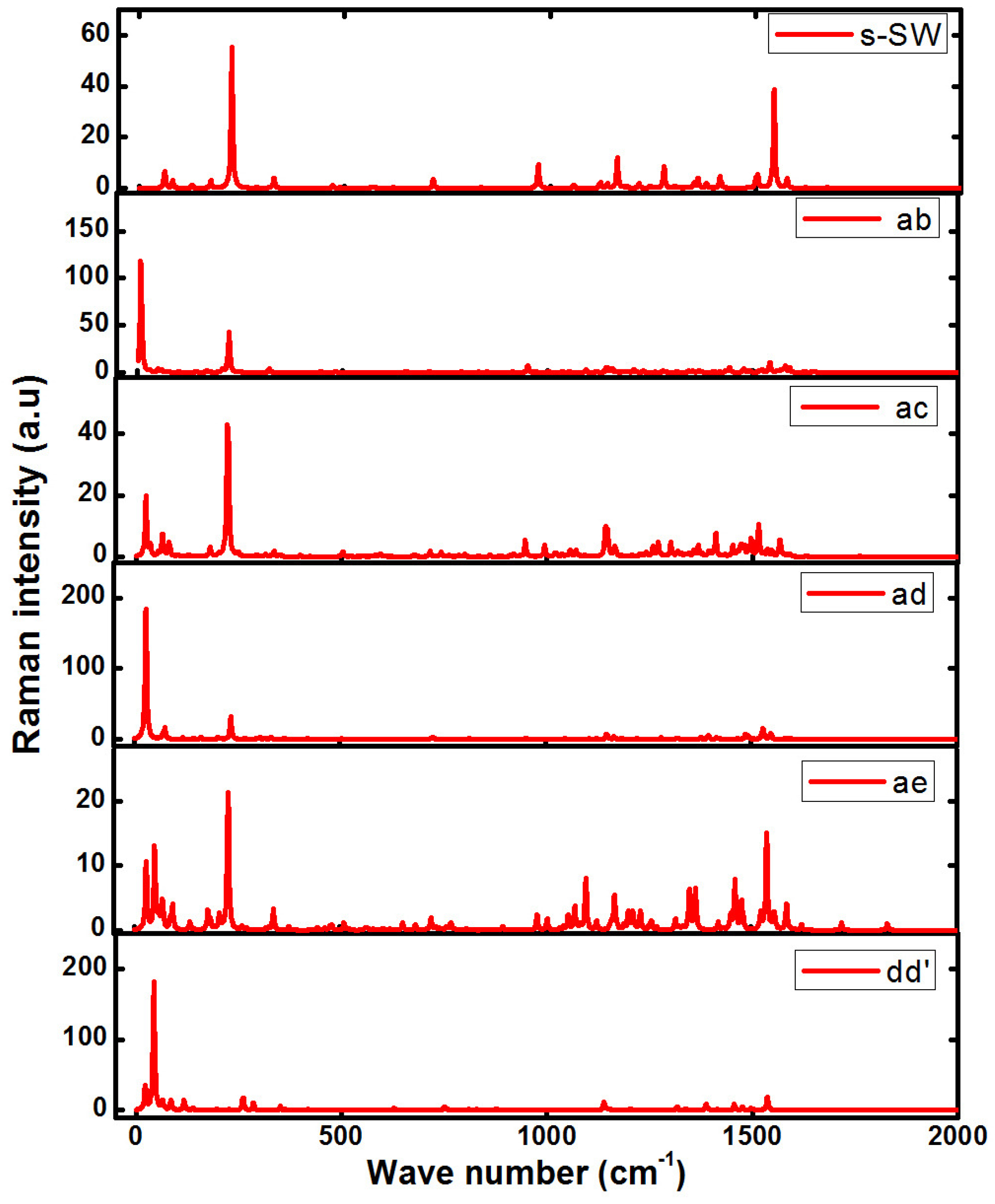
It is well established that electron confinement effect reduces with increasing size of graphene clusters and, for a system with 48 carbon (C) atoms, the bulk property predominates [16].
Motivated by this, we have chosen the graphene cluster with 48 C atoms to investigate the effect of SW defects on its vibrational and electronic properties. Note that only the middle bond has been rotated for the SW defect concentration 2.08% and, for 4.17% defect concentration, different possible positions have been indicated in Figure 1a. In Figure 1a, we have intentionally avoided the terminal bonds as defect positions for stability reasons. Therefore, the only choices to obtain 4.17% defect are ‘ab’, ‘ac’, ‘ad’, ‘ae’, ‘af’ and ‘dd ’. Other possibilities have been declined due to symmetry arguments. In addition, the ground state geometry reveals that, similar to ‘ae’, the ‘af’ system (indicated in Figure 1a) also introduces tetragon into the structure (shown in Table 1), which also reduces the stability of the system.
It is clear from Figure 1b that the optimized length of the middle bond reduces from 1.41 Å to 1.35 Å after rotation, whereas the bond ‘d’ or ‘d ’ gets a little elongated to 1.43 Å during this process. The SW defects, however, do not alter the total number of electrons in the system. Therefore, the total energy will be a crucial parameter to compare their relative stabilities. We have observed that the total energy of the system increases by an amount of 3.15 eV after the incorporation of a 2.08% SW defect into the pristine cluster. We have further compared their respective dimensions. It is notified that the distance between terminal C atoms along the direction parallel to ‘a’ has been increased from 9.91 Å to 10.54 Å, while that along ’d’ contracted from 15.56 Å to 15.15 Å. This change is due to the generation of tensile and compressive stresses into the system along respective directions as a secondary effect of SW defects. This SW defect generated stress is responsible for the increase of the total energy of the system with a 2.08% SW defect. The stress in the system is further enhanced for 4.17% defect concentration. As a result, the systems undergo buckling while trying to minimize the effect of this additional stress. This supports the fact that presence of SW defects in the system has the tendency to form non-planar nanostructures due to the intrinsic rumpling in the system [52]. The effects of topological SW defects on the systems are listed in Table 1 for better understanding. It is to be noted that pristine structure exhibits the highest stability and the stability decreases with increasing defect concentrations. Two structures ‘ab’ and ‘ac’ possess the least buckling and have the highest stability, whereas the ‘ae’ structure shown in Figure 1c contains tetra-ring in the network and is the least stable structure among all.

4. Raman Spectra

In the 1st order Raman scattering process, an incident photon interacts with the system and the system radiates a photon with some other frequency. As a result, the system changes its initial vibrational state. The frequency difference between the incident and emergent photon is thus a measure of long wavelength lattice vibration. Using these frequencies, popularly known as Raman shift, the systems can be efficiently characterized. In this context, it is important to note that the IR absorption spectra also provide the same information as we will see in the next section. However, Raman spectra are more handy tools for the high frequency lattice vibrations. The dangling bonds of the terminal C atoms are passivated with H atoms for stability purposes [53]. The Raman spectra of the graphene cluster exhibit a prominent C-C stretching mode at 1562.22 cm 1 . This mode is similar to the characterizing G mode vibration of an s p 2 hybridized graphene sheet. In addition, there are some other modes present in the Raman spectra of the pristine system. These are the stretching modes at 1303.37 cm 1 , 1326.44 cm 1 , 1336.40 cm 1 , 1337.82 cm 1 etc. In addition, we have observed a low frequency mode at 228.79 cm 1 attributed to the out of phase contraction and expansion of the whole system. The edge atoms as well as the terminal C-H bonds also contribute in the Raman pattern. We have intentionally avoided the discussions related to the less important high frequency modes caused by the vibration of C-H bonds only. We have further explored the effect of 2.08% SW defect on the Raman spectra as depicted in Figure 2.
The G mode of the pristine structure has been observed to be slightly red shifted to 1544.21 cm 1 in the presence of the defect. Similar to the pristine structure, this mode is also prominent. Therefore, the SW defect in the system acts as an active scattering center for the Raman process. For better understanding, the nature of vibration corresponding to this G mode has been well described in Figure 3a.
Similar to the previous case, there are many other additional stretching modes at 970.36 cm 1 , 1276.38 cm 1 , 1413.21 cm 1 , 1575.89 cm 1 , etc. in the Raman spectra. In addition, a mode at 1504.42 cm 1 needs special attention due to the atomic vibrations perpendicular to unrotated bonds. The low frequency mode associated with the out of phase contraction and expansion of the whole system has also been identified for the defected structure. This mode gets softened to the value 224.77 cm 1 for a 2.08% SW defect.
We have calculated the intensity ratio of the low frequency mode to the G mode before and after the introduction of defect. This ratio for the defected structure (1.18) is smaller than that of the pristine structure (1.34). There is a mode at 1138.31 cm 1 corresponding to the pendulum like oscillation of the rotated bond. In addition, there is a mode due to the solo contribution of the rotated bond at 1674.04 cm 1 as depicted in Figure 3b. This mode is the maximum frequency mode due to the vibration of C atoms of the structure. The same phenomenon has been previously observed in the case of graphene sheet with a 2.04% SW defect [54]. Absence of out of plane vibrational modes in Raman spectra strongly supports the stability of both the systems. The Raman spectra have been considerably modified with increasing defect concentration (4.17%). In addition, the Raman pattern is also very sensitive to the specific position of the defect in the system. It is evident from Figure 4 that the mode near 224.77 cm 1 is almost robust for all the systems.
On the other hand, the G like stretching mode with the maximum scattering activity are situated at 1541.29 cm 1 , 1513.73 cm 1 , 1528.78 cm 1 , 1537.24 cm 1 and 1535.51 cm 1 for ‘ab’, ‘ac’, ‘ad’, ‘ae’ and ‘dd ’, respectively. It is clear from the above data that the G band for the most stable structure ‘ab’ remains almost unaltered. On the contrary, the Raman spectra of the least stable structure ‘ae’ exhibit several low intense modes with comparable intensities [16]. The mode (1674.04 cm 1 ) due to the solo contribution of the SW defect has been found to be blue shifted to 1830.66 cm 1 for the ‘ae’ system. This shift is because of the change in electrical polarizability of the system in the presence of the tetragon. The structure ‘dd ’ has however been obtained by creating two 2.08 % SW defects at large (7.98 Å) distance as shown in Table 1. Therefore, we have compared the Raman spectra of 2.08% SW defect with ‘dd ’. The G band of the structure is at 1535.51 cm 1 , which is red shifted compared to the s-SW structure. In addition, two new low frequency modes at 22.65 cm 1 and 43.08 cm 1 have been observed in case of dd . It is worth noting that these modes are torsional and bending modes, respectively. Therefore, the appreciable number of non-stretching modes for the dd system establishes relatively less stability of the structure. In addition, a 224.77 cm 1 mode of the s-SW system is completely suppressed in dd because of large buckling produced in dd structure. Most interestingly, a mode at 1615.45 cm 1 is identified as a solo stretching mode of two rotated bonds. This mode is red shifted compared to the similar mode of s-SW structure. These results help us to interpret that 7.98 Å is the minimum distance between two SW defects required to get the signature of two distinct defects separately. The assignments of different Raman active vibrational modes are listed in the supplementary document for convenience.

5. IR Spectra

IR spectroscopy is also a very efficient tool to determine the structural details for characterization. The absorption bands of this spectra possess the information about the nature of vibration of different bonds. These vibrational modes are discrete and when the frequency of the incident photon matches with any one of these fundamental modes, they undergo absorption. The IR spectra can be classified in three frequency regions near IR (14,000–4000 cm 1 ), mid IR (4000–400 cm 1 ) and far IR (400–10 cm 1 ). In this section, we have mainly explored the mid and far IR fingerprints of the SW defects in graphene quantum dots. For better understanding, the IR spectra of all the systems are depicted in the supplementary document.
Most of the IR modes of pristine GQD have been observed to be red shifted in the presence of s-SW defect. For example, the mode corresponding to the maximum absorption is at 1604.75 cm 1 for GQD, whereas the same for s-SW system is 1674.04 cm 1 . We have further explored the low intense absorption peak due to the solo contribution of the defected bond is at 1674.04 cm 1 . Additionally, some new IR active modes have been observed for the defected system. The maximum absorption peaks for the structures with 4.17% doping concentration are at 884.25 cm 1 (ab), 873.54 cm 1 (ac), 876.88 cm 1 (ad), 1522.78 cm 1 (ae) and 863.28 cm 1 (dd ). Therefore, these systems can also be characterized with the help of IR spectroscopy. It is interesting that we have successfully identified the IR absorption frequency corresponding to the simultaneous stretching of two individual SW defects of dd at 1619.29 cm 1 . Similar to the Raman case, this also supports the fact that 7.98 Å is the minimum distance for two SW defects in graphene for their distinct existence.

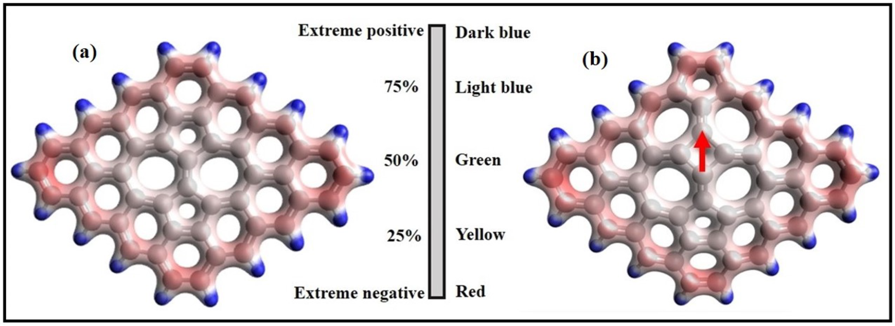
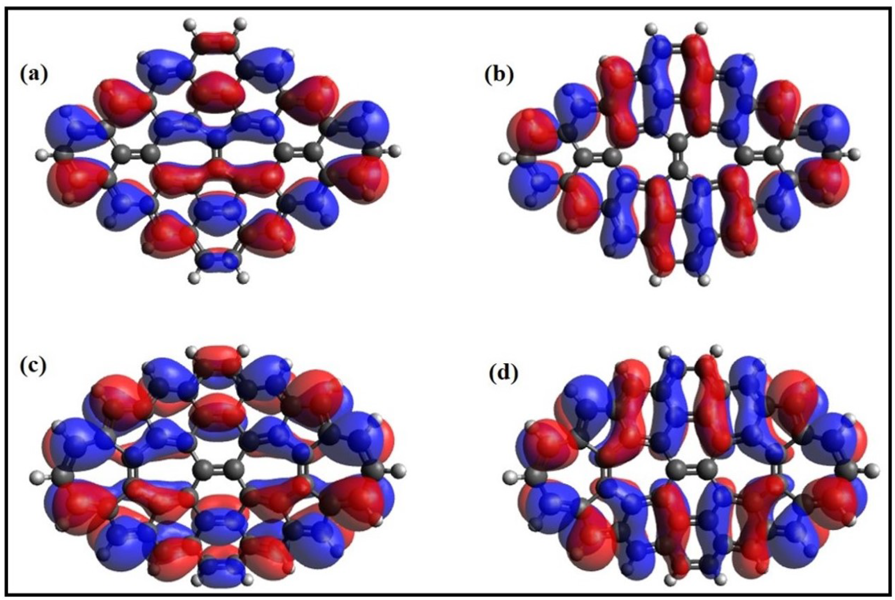
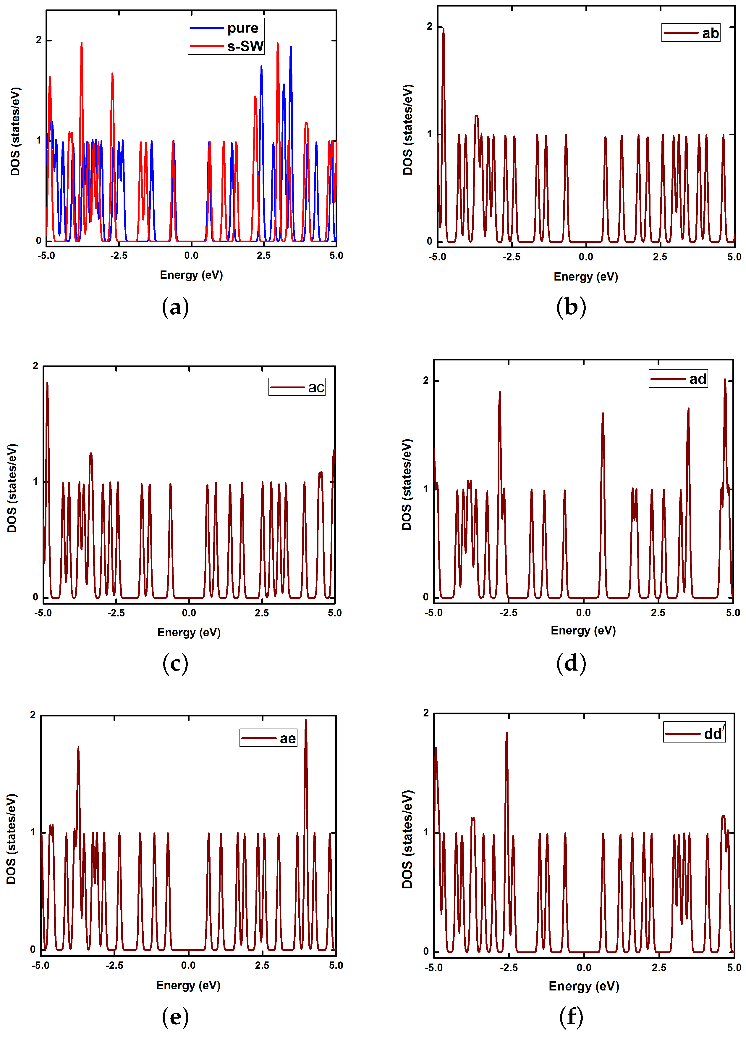
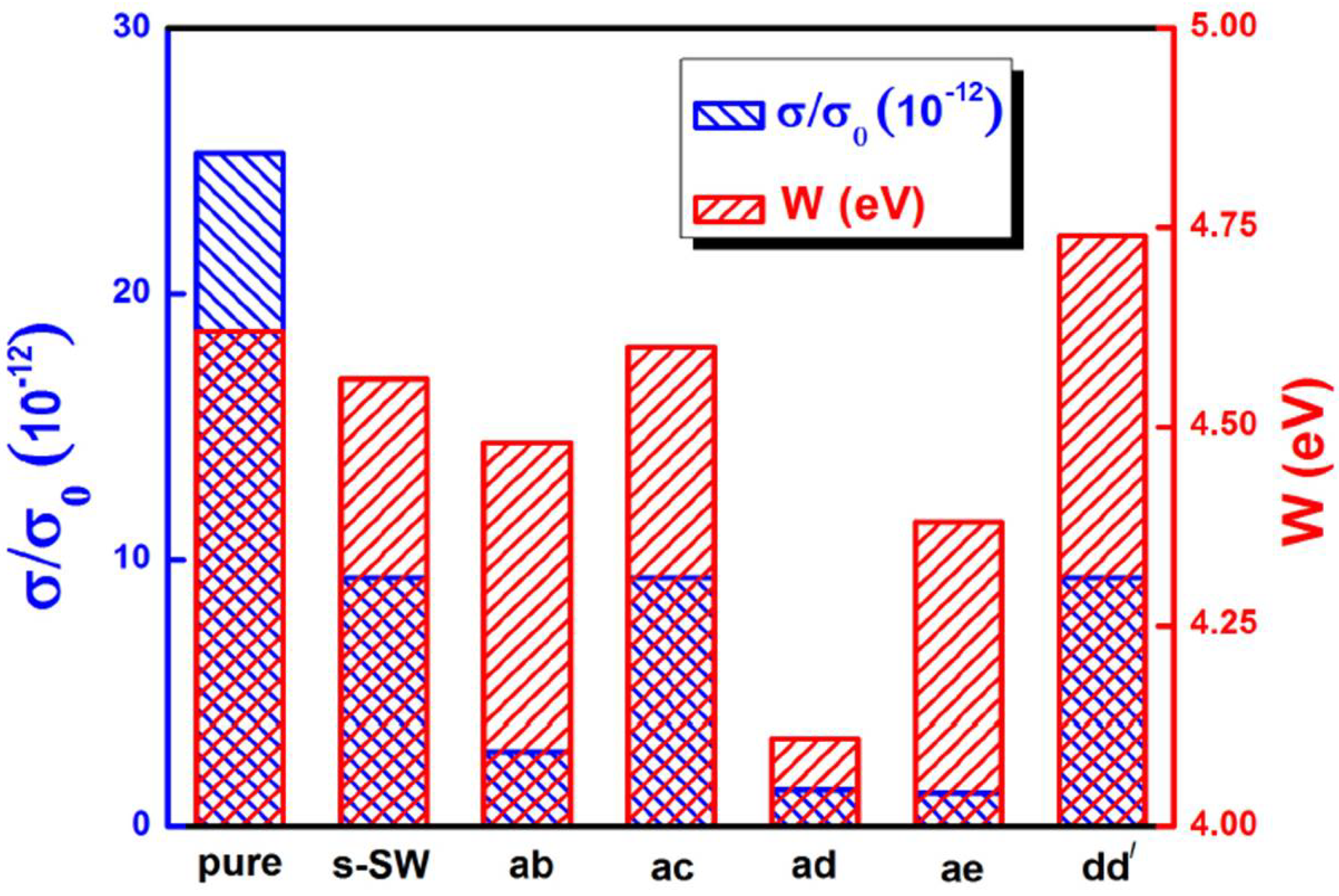
6. Electronic Properties

The anisotropic and electronic properties perturbed by the topological SW defects are discussed in this section. The importance of dipole moment is of immense help for determining related transport, chemical reactivity and opto-electronic properties of any system. It has been observed that the presence of SW defects affects the charge distribution and hence the dipole moment of the systems as listed in Table 2.
It is clear from Table 2 that finite dipole moments have been induced in the otherwise non-polar system due to the presence of SW defects. The magnitude of dipole moment varies with concentration as well as distance between the defects. The charge density and direction of the dipole moment has been depicted in Figure 5. It is observed from Figure 5 that the charges are accumulated more in the left and right end of the systems.
This is because of the maximum value of local curvature near these two points. The ‘ae’ structure possesses the highest dipole moment. As an important note, the band gap of this structure is also maximum. In addition, ‘ac’ and ‘ab’ systems also exhibit appreciable dipole moments. Here, another important note is that the dd structure has the minimum dipole moment among all 4.17% defected systems. This is due to the fact that the separation of SW defects has the maximum value in dd structure. All these finite and appreciable values of dipole moment can attain the minimum requirement for any polar gas sensors [44,55,56].
The electronic properties essentially depend on DOS near E F of the systems. Not only that, the HOMO-LUMO gap in this regard plays a vital role in deciding appropriate opto-electronic properties and chemical stability of the systems. We have thus explored the electronic state of the systems by computing the DOS corresponding to different discrete molecular levels as shown in Figure 6. For better comparison, Fermi energy (E F ≈ (E L U M O + E H O M O )/2) of the system is set to zero. Two systems ab and ac with 4.17% defect concentration possess a higher degree of stability and exhibit zero DOS at E F similar to the pristine and s-SW defect case. Figure 6a reveals that the nature of DOS near E F remains almost similar for pristine and s-SW structure.
In addition, the identification of HOMO-LUMO levels in the defected systems is also essential for designing opto-electronic devices. Therefore, the positions of the HOMO and LUMO orbitals of s-SW and dd structures are given in Figure 7. It is observed that there are no LUMO orbitals in the C atoms situated on the principal axis (parallel to the bond ‘a’) for both the systems. On the contrary, HOMO levels are observed on the rotated C dimers and their neighbouring C atoms of both the systems. We have further calculated the electrical conductivity ( σ ) of the systems from the following Equation (4)
σ = σ 0 e Δ E 2 k T .
Here, σ 0 , k and T represent the proportionality constant, Boltzmann constant and temperature, respectively. These values of electrical conductivity essentially depend on the energy difference of the discrete molecular levels near E F . It is really important to obtain the information about electron scattering through the medium. We have observed that the room temperature conductivity of the s-SW structure is 0.37 times that of the pristine structure, whereas, for the 4.17% defect concentration, the structures ‘ac’ and ‘dd ’ exhibit similar conductivity as s-SW because of the similar values of the HOMO-LUMO gaps, whereas the conductivity of ‘ab’ is 0.11 times that of the pristine system or 0.3 times that of the s-SW system. Careful observation, however, indicates that the pristine system possesses the highest conductivity and the system ‘ab’ shows the least conductivity. The reason for this low conductivity of ‘ab’ is as follows. The electrons encounter more scattering due to the structural defomation of this structure.
To explore the possibility of thermionic emission, we have now explored the variations of work function (W) with concentration and distance between the defects. For clear understanding, these values are plotted with the conductivity data in Figure 8. The values of W are relatively high for all the structures. The value of W generally decreases in the presence of SW defect. The only exception is the ’dd ’ where the value of W is greater than the pristine structure. These results will be important related to the study of possible applications of these systems in electrical devices.

7. Conclusions

A systematic investigation of geometric structure, Raman spectra, IR spectra and electronic properties of the graphene quantum dot with different SW defects have been presented in this paper under the framework of DFT. The stress has been developed due to the presence of 2.08% SW defect in the graphene network. As a consequence, the G mode (1562.22 cm 1 ) has been found to be red shifted to 1544.21 cm 1 after incorporation of a defect. The specific nature of the atomic vibrations responsible for this new G mode vibration has been identified in this paper. In addition to that, low frequency out of phase vibration of the whole system is also found to be softened from 228.79 cm 1 to 224 cm 1 after incorporation of the defect. Another high frequency peak at 1674.04 cm 1 has been recognized as a characterizing mode caused by the solo contribution of the defected bond. The stability of the systems decreases with increasing SW defect concentrations. In addition, the relative stabilities of the systems for a particular SW defect concentration (4.17%) also depend upon the separation between the defects. We have thus explored the most stable defect positions (‘ab’ and ‘ac’) for 4.17% doping concentration. The DOS spectra reveal the absence of DOS at E F for all these defected structures similar to the pristine system. The electrical conductivity has been observed to be reduced in the presence of SW defects. In addition, the value of work function generally decreases in the presence of SW defects. However, ‘dd ’ possesses a greater value of it as an exception. As a special note, the Raman spectra of the system with two SW defects separated at a distance 7.98 Å possess a mode at 1615.45 cm 1 that can be identified as the signature benchmark related to the collective effect of two individual SW defects only. This result has been well supported by the existence of the same mode in IR spectra at 1619.29 cm 1 . Therefore, this distance can be thought of as a minimum distance (separation) for which two SW defects can exhibit independent behaviour. Our study will be very effective to characterize the different types of SW defects into the experimental systems.

Author Contributions

Conceptualization, G.C.; Formal Analysis, G.C., A.B. and D.J.; Writing—Original Draft Preparation, A.B.; Supervision, Writing—Review & Editing, D.J.

Funding

This work is partially supported by DST-FIST, DST-PURSE, the Government of India.

Acknowledgments

One of the authors (A.B.) wants to thank University of Calcutta for the university research fellowship. We want to acknowledge anonymous reviewers for their critical comments and suggestions to improve the quality of the paper.

Conflicts of Interest

The authors declare no conflict of interest.

References

  1. Geim, A.K.; Novoselov, K.S. The rise of graphene. Nat. Mater. 2007, 6, 183. [Google Scholar] [CrossRef] [PubMed]
  2. Neto, A.H.C.; Guinea, F.; Peres, N.M.R.; Novoselov, K.S.; Geim, A.K. The electronic properties of graphene. Rev. Mod. Phys. 2009, 81, 109. [Google Scholar] [CrossRef]
  3. Nath, P.; Chowdhury, S.; Sanyal, D.; Jana, D. Ab-initio calculation of electronic and optical properties of nitrogen and boron doped graphene nanosheet. Carbon 2014, 73, 275. [Google Scholar] [CrossRef]
  4. Gui, G.; Li, J.; Zhong, J. Band structure engineering of graphene by strain: First-principles calculations. Phys. Rev. B 2008, 78, 075435. [Google Scholar] [CrossRef]
  5. Nath, P.; Sanyal, D.; Jana, D. Semi-metallic to semiconducting transition in graphene nanosheet with site specific co-doping of boron and nitrogen. Phys. E 2014, 56, 64. [Google Scholar] [CrossRef]
  6. Jana, D.; Nath, P.; Sanyal, D. Modifications of electronic properties of graphene by boron (B) and nitrogen (N) substitution. In Graphene Science Handbook, Nanostructure and Atomic Arrangements; Aliofkhazraei, M., Ali, N., Milne, W.I., Ozkan, C.S., Mitura, S., Gervasoni, J.L., Eds.; CRC Press: New York, NY, USA, 2016. [Google Scholar]
  7. Chowdhury, S.; Das, R.; Nath, P.; Sanyal, D.; Jana, D. Electronic and optical properties of boron and nitrogen functionalizad graphene nanosheet. In Chemical Functionalization of Carbon Nano-Materials: Chemistry and Applications; Thakur, V.K., Thakur, M.K., Eds.; CRC Publications: New York, NY, USA, 2015. [Google Scholar]
  8. Chowdhury, S.; Jana, D. A theoretical review on electronic, magnetic and optical properties of silicene. Rep. Prog. Phys. 2016, 79, 126501. [Google Scholar] [CrossRef] [PubMed]
  9. Chowdhury, S.; Bandyopadhyay, A.; Dhar, N.; Jana, D. Optical and magnetic properties of free-standing silicene, germanene and T-graphene system. Phys. Sci. Rev. 2017, 2, 0102. [Google Scholar]
  10. Yan, X.; Cui, X.; Li, L.-S. Synthesis of large, stable colloidal graphene quantum dots with tunable size. J. Am. Chem. Soc. 2010, 132, 5944. [Google Scholar] [CrossRef]
  11. Li, X.L.; Wang, X.R.; Zhang, L.; Lee, S.W.; Dai, H.J. Chemically derived, ultrasmooth graphene nanoribbon semiconductors. Science 2008, 319, 1229. [Google Scholar] [CrossRef]
  12. Cai, J.M.; Ruffieux, P.; Jaafar, R.; Bieri, M.; Braun, T.; Blankenburg, S.; Muoth, M.; Seitsonen, A.P.; Saleh, M.; Feng, X.; et al. Atomically precise bottom-up fabrication of graphene nanoribbons. Nature 2010, 466, 470. [Google Scholar] [CrossRef]
  13. Bandyopadhyay, A.; Nandy, A.; Chakrabarti, A.; Jana, D. Optical properties and magnetic flux-induced electronic band tuning of a T-graphene sheet and nanoribbon. Phys. Chem. Chem. Phys. 2017, 19, 21584. [Google Scholar] [CrossRef] [PubMed]
  14. Kim, S.; Hwang, S.W.; Kim, M.K.; Shin, D.Y.; Shin, D.H.; Kim, C.O.; Yang, S.B.; Park, J.H.; Hwang, E.; Choi, S.-H.; et al. Anomalous behaviors of visible luminescence from graphene quantum dots: Interplay between size and shape. ACS Nano 2012, 6, 8203. [Google Scholar] [CrossRef] [PubMed]
  15. Ritter, K.A.; Lyding, J.W. The influence of edge structure on the electronic properties of graphene quantum dots and nanoribbons. Nat. Mater. 2009, 8, 235. [Google Scholar] [CrossRef] [PubMed]
  16. Das, R.; Dhar, N.; Bandyopadhyay, A.; Jana, D. Size dependent magnetic and optical properties in diamond shaped graphene quantum dots: A DFT study. J. Phys. Chem. Solids. 2016, 99, 34. [Google Scholar] [CrossRef]
  17. Hamilton, I.P.; Li, B.; Yan, X.; Li, L. Alignment of colloidal graphene quantum dots on polar surfaces. Nano Lett. 2011, 11, 1524. [Google Scholar] [CrossRef]
  18. Pan, D.; Xi, C.; Li, Z.; Wang, L.; Chen, Z.; Lu, B.; Wu, M. Electrophoretic fabrication of highly robust, efficient, and benign heterojunction photoelectrocatalysts based on graphene-quantum-dot sensitized TiO2 nanotube arrays. J. Mater. Chem. 2013, 1, 3551. [Google Scholar] [CrossRef]
  19. Gupta, V.; Chaudhary, N.; Srivastava, R.; Sharma, G.D.; Bhardwaj, R.; Chand, S. Luminscent graphene quantum dots for organic photovoltaic devices. J. Am. Chem. Soc. 2011, 133, 9960. [Google Scholar] [CrossRef]
  20. Li, Y.; Zhao, Y.; Cheng, H.; Hu, Y.; Shi, G.; Dai, L.; Qu, L. Nitrogen-Doped Graphene Quantum Dots with Oxygen-Rich Functional Groups. J. Am. Chem. Soc. 2012, 134, 15. [Google Scholar] [CrossRef]
  21. Dong, Y.; Chen, C.; Zheng, X.; Gao, L.; Cui, Z.; Yang, H.; Guo, C.; Chi, Y.; Li, C.M. One-step and high yield simultaneous preparation of single-and multi-layer graphene quantum dots from CX-72 carbon black. J. Mater. Chem. 2012, 22, 8764. [Google Scholar] [CrossRef]
  22. Sun, H.; Wu, L.; Gao, N.; Ren, J.; Qu, X. Improvement of photoluminescence of graphene quantum dots with a biocompatible photochemical reduction pathway and its bioimaging application. ACS Appl. Mater. Interfaces 2013, 5, 1174. [Google Scholar] [CrossRef]
  23. Zhao, H.; Chang, Y.; Liu, M.; Gao, S.; Yu, H.; Quan, X. A universal immunosensing strategy based on regulation of the interaction between graphene and graphene quantum dots. Chem. Commun. 2013, 49, 234. [Google Scholar] [CrossRef]
  24. Ran, X.; Sun, H.; Pu, F.; Ren, J.; Qu, X. Ag nanoparticle-decorated graphene quantum dots for label-free, rapid and sensitive detection of Ag+ and biothiols. Chem. Commun. 2013, 49, 1079. [Google Scholar] [CrossRef]
  25. Bai, J.M.; Zhang, L.; Liang, R.P.; Qiu, J.D. Graphene quantum dots combined with europium ions as photoluminescent probes for phosphate sensing. Chem. Eur. J. 2013, 19, 3822. [Google Scholar] [CrossRef] [PubMed]
  26. Hashimoto, A.; Suenaga, K.; Gloter, A.; Urita, K.; Iijima, S. Direct evidence for atomic defects in graphene layers. Nature 2004, 430, 870. [Google Scholar] [CrossRef]
  27. Meyer, J.C.; Geim, A.K.; Katsnelson, M.I.; Novoselov, K.S.; Booth, T.J.; Roth, S. The structure of suspended graphene sheets. Nature 2007, 446, 60. [Google Scholar] [CrossRef] [PubMed]
  28. Fasolino, A.; Los, J.H.; Katsnelson, M.I. Intrinsic ripples in graphene. Nat. Mater. 2007, 6, 858. [Google Scholar] [CrossRef] [PubMed]
  29. Alam, A.; Sanyal, B.; Mookerjee, A. Effect of disorder on the electronic properties of graphene: A theoretical approach. Phys. Rev. B 2012, 86, 085454. [Google Scholar] [CrossRef]
  30. Sadhukhan, B.; Nayak, A.; Mookerjee, A. Effect of random vacancies on the electronic properties of graphene and T graphene: A theoretical approach. Indian J. Phys. 2017, 91, 1541. [Google Scholar] [CrossRef]
  31. Chowdhury, S.; Baidya, S.; Nafday, D.; Halder, S.; Kabir, M.; Sanyal, B.; Saha-Dasgupta, T.; Jana, D.; Mookerjee, A. A real-space study of random extended defects in solids: Application to disordered Stone–Wales defects in graphene. Phys. E 2014, 61, 191. [Google Scholar] [CrossRef]
  32. Kotakoski, J.; Meyer, J.C.; Kurasch, S.; Santos-Cottin, D.; Kaiser, U.; Krasheninnikov, A.V. Stone–Wales-type transformations in carbon nanostructures driven by electron irradiation. Phys. Rev. B 2011, 83, 245420. [Google Scholar] [CrossRef]
  33. Jana, D.; Sun, C.L.; Chen, L.C.; Chen, K.H. Effect of chemical doping of boron and nitrogen on the electronic, optical, and electrochemical properties of carbon nanotubes. Prog. Mater. Sci. 2013, 58, 565. [Google Scholar] [CrossRef]
  34. Zhang, W.X.; He, C.; Lia, T.; Gonga, S.B. Tuning electronic and magnetic properties of zigzag graphene nanoribbons with a Stone–Wales line defect by position and axis tensile strain. RSC Adv. 2015, 5, 33407. [Google Scholar] [CrossRef]
  35. Zhao, Y.; Lin, Y.; Yakobson, B.I. Fullerene shape transformations via Stone–Wales bond rotations. Phys. Rev. B 2003, 68, 233403. [Google Scholar] [CrossRef]
  36. Kotakoski, J.; Krasheninnikov, A.V.; Kaiser, U.; Meyer, J.C. From point defects in graphene to two-dimensional amorphous carbon. Phys. Rev. Lett. 2011, 106, 105505. [Google Scholar] [CrossRef] [PubMed]
  37. Vicarelli, L.; Heerema, S.J.; Dekker, C.; Zandbergen, H.W. Controlling defects in graphene for optimizing the electrical properties of graphene nanodevices. ACS Nano 2015, 9, 3428. [Google Scholar] [CrossRef] [PubMed]
  38. Xia, F.; Farmer, D.B.; Lin, Y.; Avouris, P. Graphene field-effect transistors with high on/off current ratio and large transport band gap at room temperature. Nano Lett. 2010, 10, 715. [Google Scholar] [CrossRef] [PubMed]
  39. Kang, J.; Bang, J.; Ryu, B.; Chang, K.J. Effect of atomic-scale defects on the low-energy electronic structure of graphene: Perturbation theory and local-density-functional calculations. Phys. Rev. B 2008, 77, 115453. [Google Scholar] [CrossRef]
  40. Carlsson, J.M.; Scheffler, M. Structural, electronic, and chemical properties of nanoporous carbon. Phys. Rev. Lett. 2006, 96, 046806. [Google Scholar] [CrossRef]
  41. Lu, J.; Yeo, P.S.E.; Gan, C.K.; Wu, P.; Loh, K.P. Transforming C60 molecules into graphene quantum dots. Nat. Nanotechnol. 2011, 6, 247. [Google Scholar] [CrossRef]
  42. Malard, L.M.; Pimenta, M.A.; Dresselhaus, G.; Dresselhaus, M.S. Raman spectroscopy in graphene. Phys. Rep. 2009, 473, 51. [Google Scholar] [CrossRef]
  43. Dresslhaus, M.S.; Jorio, A.; Saito, R. Characterizing Graphene, Graphite, and Carbon Nanotubes by Raman Spectroscopy. Annu. Rev. Condens. Matter Phys. 2010, 108, 1. [Google Scholar] [CrossRef]
  44. Bandyopadhyay, A.; Paria, S.; Jana, D. Tetragonal graphene nanodot as carbon monoxide gas sensor and current rectification device. J. Phys. Chem. Solids 2018, 123, 172. [Google Scholar] [CrossRef]
  45. Cancado, L.G.; Pimenta, M.A.; Neves, B.R.A.; Dantas, M.S.; Jorio, A. Influence of the Atomic Structure on the Raman Spectra of Graphite Edges. Phys. Rev. Lett 2004, 93, 247401. [Google Scholar] [CrossRef] [PubMed]
  46. Krauss, B.; Nemes-Incze, P.; Skakalova, V.; Biro, L.P.; von Klitzing, K.; Smet, J.H. Raman scattering at pure graphene zigzag edges. Nano Lett. 2010, 10, 4544. [Google Scholar] [CrossRef] [PubMed]
  47. Frisch, M.J.; Trucks, G.W.; Schlegel, H.B. Gaussian 09 Manual. Available online: http://gaussian.com (accessed on 14 December 2018).
  48. Lee, C.; Yang, W.; Parr, R.G. Development of the Colle-Salvetti correlation-energy formula into a functional of the electron density. Phys. Rev. B 1988, 37, 785. [Google Scholar] [CrossRef]
  49. Miehlich, B.; Savin, A.; Stoll, H.; Preuss, H. Results obtained with the correlation energy density functionals of Becke and Lee, Yang and Parr. Chem. Phys. Lett. 1989, 157, 200. [Google Scholar] [CrossRef]
  50. Scott, A.P.; Radom, L. Harmonic Vibrational Frequencies: An Evaluation of Hartree–Fock, Møller–Plesset, Quadratic Configuration Interaction, Density Functional Theory, and Semiempirical Scale Factors. J. Phys. Chem. 1996, 100, 16502. [Google Scholar] [CrossRef]
  51. Boyle, N.O. GaussSum 3.0 Home Page. Available online: http://www.gausssum.sf.net (accessed on 13 December 2018).
  52. Ugarte, D. Curling and closure of graphitic networks under electron-beam irradiation. Nature 1992, 359, 707. [Google Scholar] [CrossRef]
  53. Bandyopadhyay, A.; Pal, P.; Chowdhury, S.; Jana, D. First principles Raman study of boron and nitrogen doped planar T-graphene clusters. Mater. Res. Express 2015, 2, 95603. [Google Scholar] [CrossRef]
  54. Shirodkar, S.N.; Waghmare, U.V. Electronic and vibrational signatures of Stone–Wales defects in graphene: First-principles analysis. Phys. Rev. B 2012, 86, 165401. [Google Scholar] [CrossRef]
  55. Chopra, S.; McGuire, K.; Gothard, N.; Rao, A.M. Selective gas detection using a carbon nanotube sensor. Appl. Phys. Lett. 2003, 83, 2280. [Google Scholar] [CrossRef]
  56. Nagarajan, V.; Chandiramouli, R. Investigation on adsorption properties of CO and NO gas molecules on aluminene nanosheet: A density functional application. Mater. Sci. Eng. B 2018, 229, 193. [Google Scholar] [CrossRef]
Figure 1. (a) The schematic diagram of the optimized GQD with 2.08% defect concentration. Any one of the bonds b, c, d, e, f, d can be additionally rotated to achieve 4.17% defect concentration; (b) Bond lengths and angles of the 2.08% SW defect concentration; (c) The structure ae has 4.17% defect concentration and possesses tetragon in the structure.
Condensedmatter 03 00050 g001
Figure 2. Comparison between the Raman spectra of pristine graphene cluster and 2.08% SW defect.
Condensedmatter 03 00050 g002
Figure 3. (a) Signature of the G mode vibration and (b) Solo contribution of SW defect at 1674.04 cm 1 of graphene cluster with 2.08% SW defect.
Condensedmatter 03 00050 g003
Figure 4. Raman spectra of different possible systems with 4.17% SW defect concentration. The Raman spectra for 2.08% SW defect is also given for comparison.
Condensedmatter 03 00050 g004
Figure 5. Charge density plot of (a) s-SW and (b) ae structure. The direction of the dipole moment has been shown with a red arrow. The image has been drawn with isovalue 0.01 e /au 3 .
Condensedmatter 03 00050 g005
Figure 6. Density of states spectra of (a) s-SW and pristine GQD’ (b) ab; (c) ac; (d) ad; (e) ae; and (f) dd structures. The E F of all the structures are set to zero for convenience. The full width at half maximum of the Lorentzian fitted DOS envelope is 0.1 eV.
Condensedmatter 03 00050 g006
Figure 7. (a) HOMO of s-SW; (b) LUMO of s-SW; (c) HOMO of dd ; (d) LUMO of dd . The image has been drawn with isovalue 0.01 e /au 3 .
Condensedmatter 03 00050 g007
Figure 8. Conductivity and work function for structures with different defects.
Condensedmatter 03 00050 g008
Table 1. Table for the number of non-hexagonal polygons in the systems, distance between two defect positions and the total energy E of the systems.
SystemsTetragonPentagonHeptagonOctagonDistance (Å)E (eV)
pristine0000-−50,074.06
s-SW0220-−50,070.92
ab02202.36−50,069.59
ac03303.00−50,069.01
ad04213.99−50,068.48
ae12402.82−50,067.24
dd 04407.98−50,068.52
Table 2. Table for dipole moment (D), vacuum energy level (E v ), LUMO and HOMO energies, band gap Δ E (=E L U M O (eV) − E H O M O ), and the work function W (= E v − E H O M O ).
SystemsD (debye)E v (eV)E LUMO (eV)E HOMO (eV) Δ E (eV)W (eV)
pristine00.46−2.94−4.161.224.62
s-SW0.00130.47−2.82−4.091.274.56
ab0.86190.29−2.86−4.191.334.48
ac0.98640.45−2.88−4.151.274.60
ad0.46540.02−2.84−4.091.254.11
ae1.47390.13−2.88−4.251.374.38
dd 0.15370.54−2.93−4.201.274.74

