
Magnetoresistance, Gating and Proximity Effects in Ultrathin NbN-Bi2Se3 Bilayers

Abstract
:1. Introduction
2. Experimental
2.1. Choice of the Bilayer Parameters
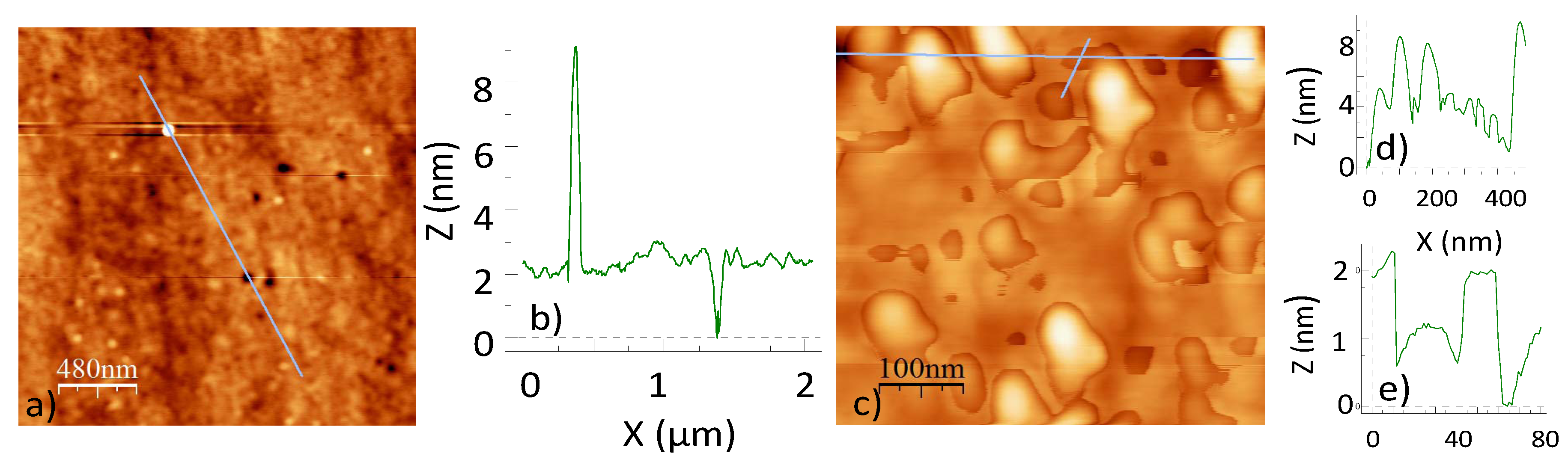
2.2. Surface Morphology of the Film and Bilayer
2.3. The Gates and Contacts Geometry
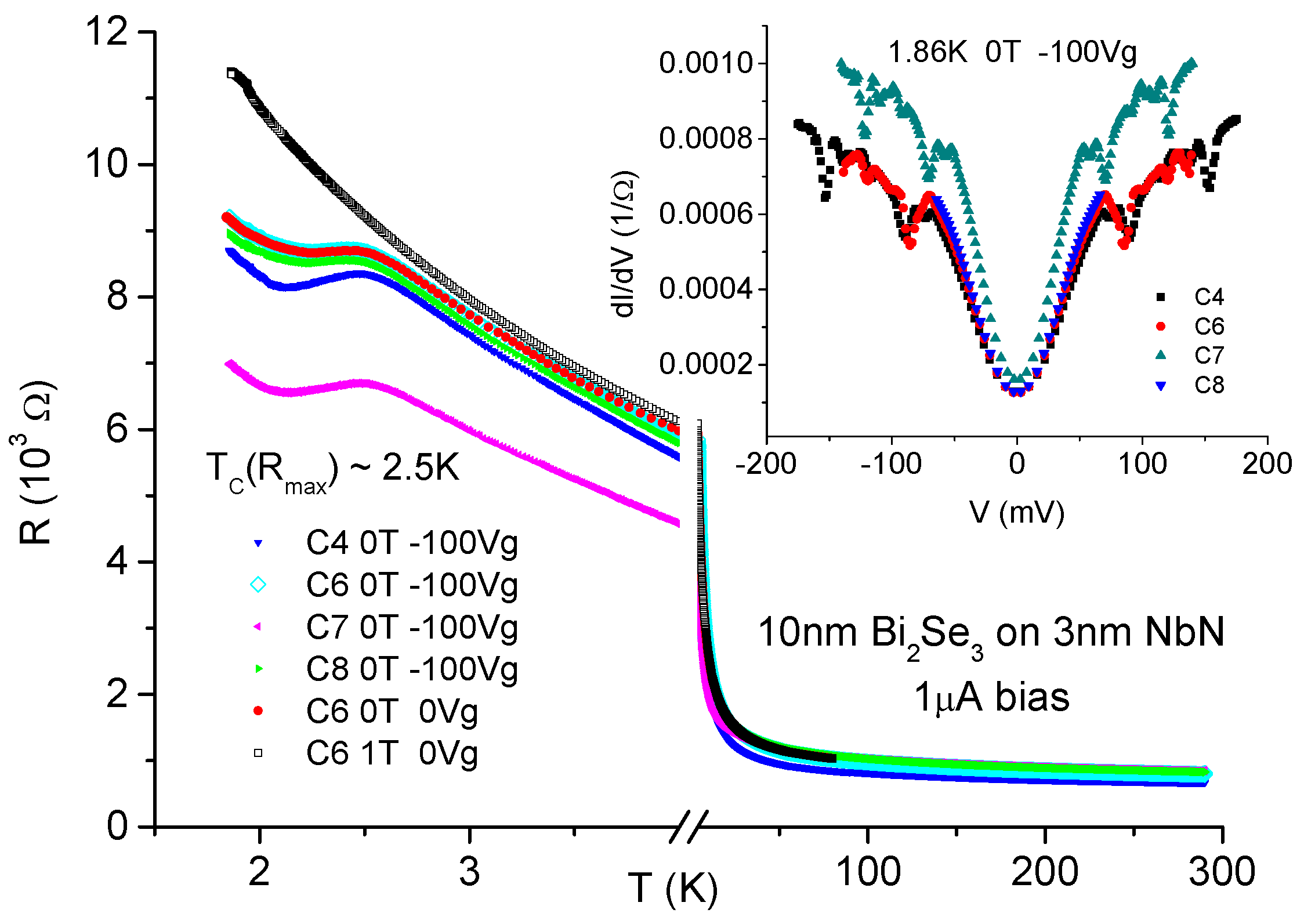
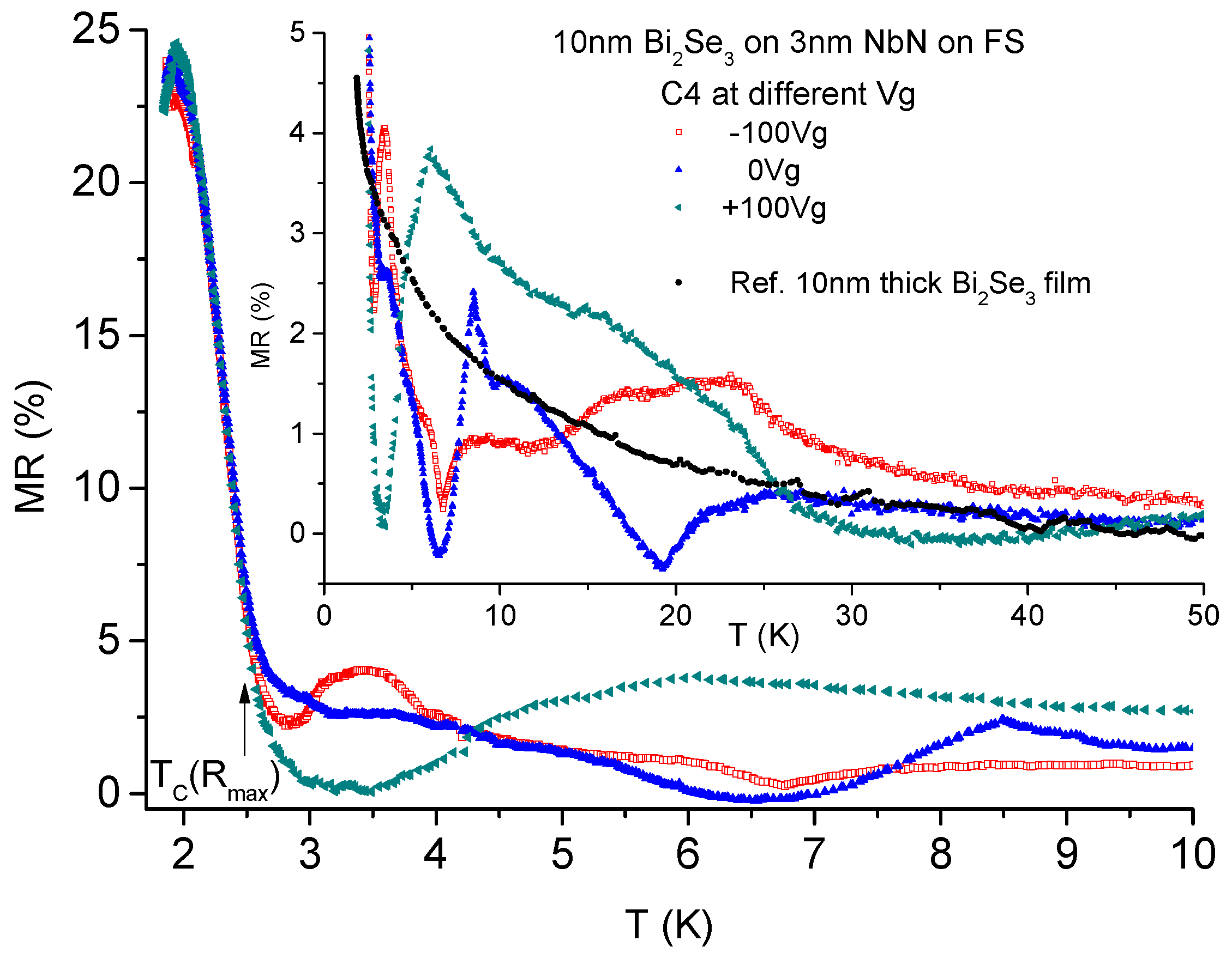
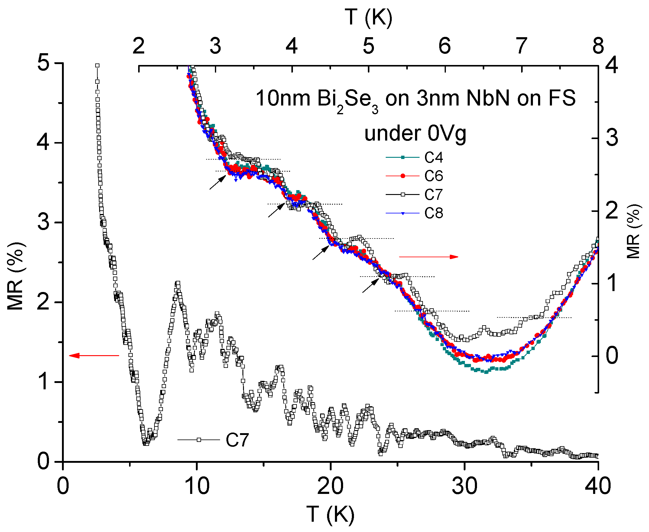
3. Results and Discussion
4. Materials and Methods
5. Conclusions
Supplementary Materials
Acknowledgments
Conflicts of Interest
References
- Hassan, M.Z.; Kane, C.L. Colloquium: Topological insulators. Rev. Mod. Phys. 2010, 82, 3045–3067. [Google Scholar] [CrossRef]
- Fu, L.; Kane, C.L. Superconducting Proximity Effect and Majorana Fermions at the Surface of a Topological Insulator. Phys. Rev. Lett. 2008, 100, 096407. [Google Scholar] [CrossRef] [PubMed]
- Pesin, D.; MacDonald, A.H. Spintronics and pseudospintronics in graphene and topological insulators. Nat. Mater. 2012, 11, 409–416. [Google Scholar] [CrossRef] [PubMed]
- Bravyi, S.B.; Kitaev, A. Fermionic quantum computation. Ann. Phys. 2002, 298, 210–226. [Google Scholar] [CrossRef]
- Kriener, M.; Segawa, K.; Ren, Z.; Sasaki, S.; Wada, S.; Kuwabata, S.; Ando, Y. Electrochemical synthesis and superconducting phase diagram of CuxBi2Se3. Phys. Rev. B 2011, 84, 054513. [Google Scholar] [CrossRef]
- Ando, Y. Topological insulator materials. J. Phys. Soc. Jpn. 2013, 82, 102001. [Google Scholar] [CrossRef]
- Guan, S.Y.; Chen, P.J.; Chu, M.W.; Sankar, R.; Chu, F.; Jeng, H.T.; Chang, C.S.; Chuang, T.M. Superconducting topological surface states in the noncentrosymmetric bulk superconductor PbTaSe2. Sci. Adv. 2016, 2, e1600894. [Google Scholar] [CrossRef] [PubMed]
- Koren, G.; Kirzhner, T.; Lahoud, E.; Chashka, K.B.; Kanigel, A. Proximity induced superconductivity by Bi in topological Bi2Te2Se and Bi2Se3 films: Evidence for a robust zero energy bound state that could be due to Majorana Fermions. Phys. Rev. B 2011, 84, 224521. [Google Scholar] [CrossRef]
- Yang, F.; Ding, Y.; Qu, F.; Shen, J.; Chen, J.; Wei, Z.; Ji, Z.; Liu, G.; Fan, J.; Yang, C.; et al. Proximity effect at superconducting Sn-Bi2Se3 interface. Phys. Rev. B 2012, 85, 104508. [Google Scholar] [CrossRef]
- Mourik, V.; Zuo, K.; Frolov, S.M.; Plissard, S.R.; Bakkers, E.P.; Kouwenhoven, L.P. Signatures of Majorana fermions in hybrid superconductor-semiconductor nanowire devices. Science 2012, 336, 1003. [Google Scholar] [CrossRef] [PubMed]
- Das, A.; Ronen, Y.; Most, Y.; Oreg, Y.; Heiblum, M.; Shtrikman, H. Zero-bias peaks and splitting in an Al-InAs nanowire topological superconductor as a signature of Majorana fermions. Nat. Phys. 2012, 8, 887–895. [Google Scholar] [CrossRef]
- Xu, J.P.; Liu, C.; Wang, M.X.; Ge, V.; Liu, Z.L.; Yang, X.; Chen, Y.; Liu, Y.; Xu, Z.A.; Gao, C.L.; et al. Artificial topological superconductor by the proximity effect. Phys. Rev. Lett. 2014, 112, 217001. [Google Scholar] [CrossRef]
- Haim, A.; Berg, E.; von Oppen, F.; Oreg, Y. Signatures of Majorana zero modes in spin-resolved current correlations. Phys. Rev. Lett. 2015, 114, 166406. [Google Scholar] [CrossRef] [PubMed]
- Kells, G.; Meidan, D.; Brouwer, P.W. Near-zero-energy end states in topologically trivial spin-orbit coupled superconducting nanowires with a smooth confinement. Phys. Rev. B 2012, 86, 100503. [Google Scholar] [CrossRef]
- Higginbotham, A.P.; Albrecht, S.M.; Kirsanskas, G.; Chang, W.; Kuemmeth, F.; Krogstrup, P.; Jespersen, T.S.; Nygard, J.; Flensberg, K.; Marcus, C.M. Parity lifetime of bound states in a proximitized semiconductor nanowire. Nat. Phys. 2015, 11, 1017–1021. [Google Scholar] [CrossRef]
- Churchill, H.O.H.; Fatemi, V.; Grove-Rasmussen, K.; Deng, M.T.; Caroff, P.; Xu, H.Q.; Marcus, C.M. Superconductor-nanowire devices from tunneling to the multichannel regime: Zero-bias oscillations and magnetoconductance crossover. Phys. Rev. B 2013, 87, 241401. [Google Scholar] [CrossRef]
- Koren, G. Proximity effects at the interface of a superconductor and a topological insulator in NbN-Bi2Se3 thin film bilayers. Supercond. Sci. Technol. 2015, 28, 025003. [Google Scholar] [CrossRef]
- Koren, G.; Kirzhner, T. Zero-energy bound states in tunneling conductance spectra at the interface of an s-wave superconductor and a topological insulator in NbN/Bi2Se3/Au thin-film junctions. Phys. Rev. B 2012, 86, 144508. [Google Scholar] [CrossRef]
- Koren, G.; Kirzhner, T.; Kalcheim, Y.; Millo, O. Signature of proximity-induced px + ipy triplet pairing in the doped topological insulator Bi2Se3 by the s-wave superconductor NbN. EPL 2013, 103, 67010. [Google Scholar] [CrossRef]
- Du, X.-K.; Wang, T.-M.; Wang, C.; Chen, B.L.; Zhou, L. Microstructure and Optical Characterization of Magnetron Sputtered NbN Thin Films. Chin. J. Aeronaut. 2007, 20, 140–144. [Google Scholar] [CrossRef]
- Zhang, Z.; Yates, J.T., Jr. Band bending in semiconductors: Chemical and physical consequences at surfaces and interfaces. Chem. Rev. 2012, 112, 5520–5551. [Google Scholar] [CrossRef] [PubMed]
- Gotoh, Y.; Tsuji, H.; Ishikawa, J. Measurements of work function of transition metal nitride and carbide thin films. J. Vac. Sci. Technol. B 2003, 21, 1607. [Google Scholar] [CrossRef]
- Takane, D.; Souma, S.; Sato, T.; Takahashi, T.; Segawa, K.; Ando, Y. Work function of bulk insulating topological-insulator Bi2-xSbxTe3-ySey. Appl. Phys. Lett. 2016, 109, 91601. [Google Scholar] [CrossRef]
- Steinberg, H.; Gardner, D.J.; Lee, Y.S.; Jarillo-Herrero, P. Surface state transport and ambipolar electric field effect in Bi2Se3 nanodevices. Nano Lett. 2010, 10, 5032–5036. [Google Scholar] [CrossRef] [PubMed]
- Steinberg, H.; Laloe, J.-B.; Fatemi, V.; Moodera, J.S.; Jarillo-Herrero, P. Electrically tunable surface-to-bulk coherent coupling in topological insulator thin films. Phys. Rev. B 2011, 84, 233101. [Google Scholar] [CrossRef]
- Koren, G.; Millo, O. Conventional proximity effect in bilayers of superconducting underdoped La1.88Sr0.12CuO4 islands coated with nonsuperconducting overdoped La1.65Sr0.35CuO4. Phys. Rev. B 2009, 80, 054507. [Google Scholar] [CrossRef]
- Kamlapure, A.; Mondal, M.; Chand, M.; Mishra, A.; Jesudasan, J.; Bagwe, V.; Benfatto, L.; Tripathi, V.; Raychaudhuri, P. Measurement of magnetic penetration depth and superconducting energy gap in very thin epitaxial NbN films. Appl. Phys. Lett. 2010, 96, 072509. [Google Scholar] [CrossRef]
- Sheet, G.; Mukhopadhyay, S.; Raychaudhuri, P. Role of critical current on the point-contact Andreev reflection spectra between a normal metal and a superconductor. Phys. Rev. B 2004, 69, 134507. [Google Scholar] [CrossRef]
- Oudenaarden, A.; Devoret, M.H.; Nazarov, Y.V.; Mooij, J.E. Magneto-electric Aharonov-Bohm effect in metal rings. Nature 1998, 391, 768–770. [Google Scholar] [CrossRef]
- Huefner, M.; Molitor, M.; Jacobsen, A.; Pioda, A.; Stampfer, C.; Ensslin, K.; Ihn, T. The Aharonov-Bohm effect in side-gated graphene ring. New J. Phys. 2010, 12, 043054. [Google Scholar] [CrossRef]
- Koren, G.; Millo, O. Enhancement of the superconducting transition temperature of La2-xSrxCuO4 and La1.875Ba0.125CuO4 bilayers: Bilayer and reference film prepared on the same wafer. Phys. Rev. B 2010, 81, 134516. [Google Scholar] [CrossRef]
- Kirzhner, T.; Lahoud, E.; Chaska, K.B.; Salman, Z.; Kanigel, A. Point-contact spectroscopy of Cu0.2Bi2Se3 single crystals. Phys. Rev. B 2012, 86, 064517. [Google Scholar] [CrossRef]
- Wang, Y.; Li, L.; Ong, N.P. Nernst effect in high-Tc superconductors. Phys. Rev. B 2006, 73, 024510. [Google Scholar] [CrossRef]
- Liu, T.; Franz, M. Electronic structure of topological superconductors in the presence of a vortex lattice. Phys. Rev. B 2015, 92, 134519. [Google Scholar] [CrossRef]
- Darlinski, A.; Halbritter, J. Angle-resolved XPS Studies of Oxides at NbN, NbC, andl Nb Surfaces. Surf. Interface Anal. 1987, 10, 223–237. [Google Scholar] [CrossRef]


© 2017 by the author. Licensee MDPI, Basel, Switzerland. This article is an open access article distributed under the terms and conditions of the Creative Commons Attribution (CC BY) license (http://creativecommons.org/licenses/by/4.0/).
Share and Cite
Koren, G. Magnetoresistance, Gating and Proximity Effects in Ultrathin NbN-Bi2Se3 Bilayers. Condens. Matter 2017, 2, 14. https://doi.org/10.3390/condmat2020014
Koren G. Magnetoresistance, Gating and Proximity Effects in Ultrathin NbN-Bi2Se3 Bilayers. Condensed Matter. 2017; 2(2):14. https://doi.org/10.3390/condmat2020014
Chicago/Turabian StyleKoren, Gad. 2017. "Magnetoresistance, Gating and Proximity Effects in Ultrathin NbN-Bi2Se3 Bilayers" Condensed Matter 2, no. 2: 14. https://doi.org/10.3390/condmat2020014
APA StyleKoren, G. (2017). Magnetoresistance, Gating and Proximity Effects in Ultrathin NbN-Bi2Se3 Bilayers. Condensed Matter, 2(2), 14. https://doi.org/10.3390/condmat2020014