Abstract
In this study, the effects of specific power (1–100 W/cm2), operating pressure (0.5–3.0 Pa), and voltage frequency (20–500 kHz) on film growth kinetics, morphology, and silicon entrainment were investigated to optimize magnetron sputtering for producing thin silicon films suitable for lithium-ion battery anodes. Silicon films were deposited on copper substrates using the Caroline D12C system. The film thickness and morphology were determined using scanning electron microscopy and atomic force microscopy. It was found that the porosity of the films increases with increasing pressure in the working chamber. It was found that the film morphology is non-uniform up to a thickness of 100–150 nm. After that, the film thickness becomes uniform over the entire substrate surface, and the deposition rate increases sharply, i.e., an induction period is observed. The induction period duration decreases with increasing voltage power and frequency. At the same time, silicon removal increases. Frequency has a greater effect on both parameters. The paper specifies a strategy for the technical and economic optimization of the magnetron sputtering process, which determines a compromise between the positive effect of increasing productivity and the negative effect of silicon removal.
1. Introduction
A special class of film-based structures are silicon films. They may contain various polymorphic modifications of silicon, such as amorphous, crystalline, and nanocrystalline silicon. In addition to silicon, such films can include impurity components such as oxygen, carbon, hydrogen, nitrogen, metal atoms, etc. [1].
Depending on the properties of silicon films—their structure, morphology, thickness, doping with impurity components, production technology, manufacturing complexity and production cost—they can be used in various fields of technology, ranging from photovoltaic cells to gas sensors. The above applications involve very small amounts of silicon transfer during the production process. In this regard, silicon-based thin films have been successfully prepared using chemical vapor deposition (CVD), magnetron sputtering, and vacuum evaporation [2,3,4].
More recently, a new area of application for thin-film silicon structures has emerged: the production of anodes for commercial lithium-ion batteries (LIB). The specific capacity of LIB anodes made of graphite for commercial lithium-ion batteries has been increased to the highest possible value. This figure is close to the theoretical value—372 mAh/g. One option to increase LIB capacity is to switch to materials that can store more lithium than carbon-based materials. Many researchers consider silicon and its polymorphic modifications to be the most promising materials. This is due to the fact that the theoretical specific capacity of silicon for lithium is 4200 mAh/g [5,6,7,8].
According to current LIB manufacturing technologies, the creation of silicon films is carried out by spreading a suspension of silicon powder with the addition of binders onto the surface of the substrate. After this, drying and subsequent production operations are carried out. However, such films are not nano-sized, because their thickness reaches tens and hundreds of micrometers. The lithiation process of the silicon anode during LIB charging is limited by the diffusion of ions in the anode volume, so a large film thickness leads to an increase in battery charging time. Meanwhile, modern equipment and technologies require a radical reduction in the charging time of rechargeable chemical current sources and an increase in the number of charge–discharge cycles with minimal loss of battery electrical capacity. This can be achieved by reducing the thickness of the silicon anode. To prevent a decrease in the total charge storage capacity, a multilayer battery can be created with alternating multiple layers of nano-sized cathode and anode films in one housing [9].
A difficulty with this solution is the low productivity of existing equipment for growing thin nano-sized films. The existing capabilities of transferring materials to a substrate using laser epitaxy, magnetron sputtering, and vapor deposition are sufficient to solve problems in the production of microelectronics but are not enough for the mass production of high-energy capacity LIBs. In this regard, studying the kinetics of growing thin nanosized silicon films and identifying possibilities for accelerating this process become relevant.
2. Results and Discussion
The morphology of the surface of a silicon film during the stationary period of magnetron sputtering. The morphology of silicon film obtained by magnetron sputtering is an important characteristic that determines its properties and suitability for various fields of film application.
At the initial stage of the research, experiments were carried out at a fixed specific power on the target—1 W/cm2 with a constant, pulseless voltage supply and a distance from the target to the substrate of 7 cm. At certain intervals, the morphology of the resulting silicon film was studied, and its thickness was assessed. The results of the study are presented in Figure 1.
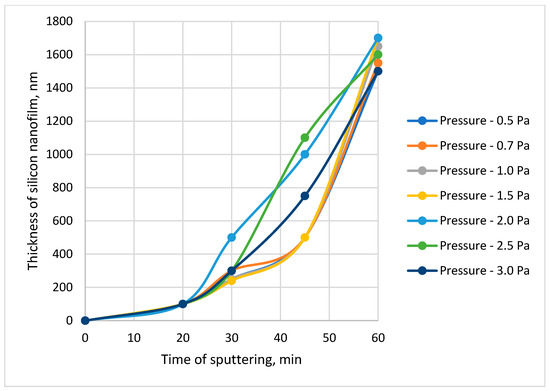
Figure 1.
Kinetic curves of thickness growth of silicon nanofilms during magnetron sputtering, specific power on the target—1 W/cm2, pulseless voltage supply, distance from target to substrate 7 cm.
During the study, it was found that up to a film thickness of 100 nm (20 min from the start of the process), the morphology of the film is heterogeneous. The density of particle formation on the substrate is uneven. Particle agglomerations take place. There are areas of the substrate that do not contain silicon particles.
The conventional rate of film formation is 5 nm/min. After the formation of a continuous film surface, the growth rate of the film thickness increases sharply to 35–40 nm/min. This speed is typical for all pressure values in the working chamber. This indicates that within 20 min for all operating pressures in the chamber, silicon condensation centers appear from the plasma flow. Around these centers, further intensification of film growth occurs. This period is called the induction period of the process.
After the completion of the induction period of film formation and the transition to a stationary growth mode, the kinetic curves acquire a specific form, different for different pressure values in the working chamber. The nature of the kinetic curves of film thickness growth in stationary mode is exponential for low (0.5–1.5 Pa) and high (3.0 Pa) pressures, and linear for the middle range (2.0–2.5 Pa). Mathematical models describing kinetic curves and approximation reliability values (R2) for various pressure values in the working chamber are presented in Table 1.

Table 1.
Mathematical models describing the kinetic curves of magnetron sputtering (Figure 1) and the values of approximation reliability for various pressure values in the working chamber.
Figure 2, Figure 3, Figure 4 and Figure 5 show the results of studies carried out on a scanning electron microscope Jeol.
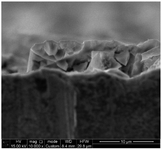
Figure 2.
Images of the surface of silicon nanofilms in the final stage of the stationary growth mode at pressure in the working chamber—0.5 Pa.
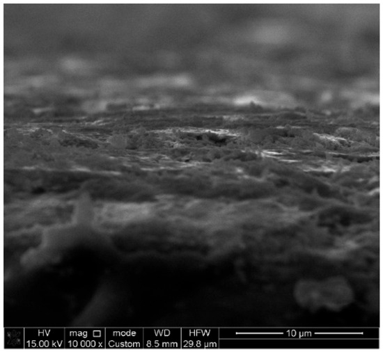
Figure 3.
Images of the surface of silicon nanofilms in the final stage of the stationary growth mode at pressure in the working chamber—1.0 Pa.
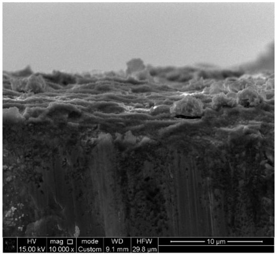
Figure 4.
Images of the surface of silicon nanofilms in the final stage of the stationary growth mode at pressure in the working chamber—2.0 Pa.
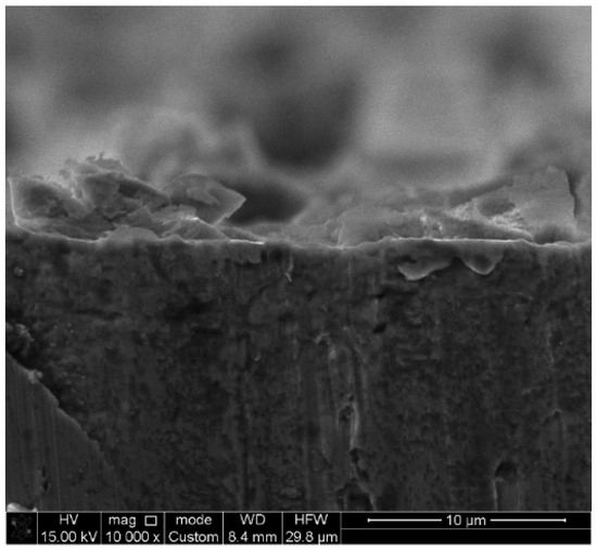
Figure 5.
Images of the surface of silicon nanofilms in the final stage of the stationary growth mode at pressure in the working chamber—3.0 Pa.
JSM-6490 LA, with the help of which the thickness of silicon nanofilms obtained in the final stage of the stationary period of magnetron sputtering was assessed.
As can be seen from Figure 2, Figure 3, Figure 4 and Figure 5, the pressure in the working chamber does significantly affect the structure of the silicon nanofilm. In all variants of the study, the adhesion of silicon particles to the substrate is high, the distribution over the surface (prior to the study, the substrate was previously treated with sandpaper with an average grain size of 200 µm).
We have conducted initial studies in the field of long-term stability of the nanofilms we have obtained. In particular, we selectively assessed the adhesion of the nanofilms to the substrate. It is fundamentally important that the film adhesion is strong enough to prevent delamination of the cathode and anode system of the LIB. The adhesion variability ranged from 9 to 12 MPa. This is a good enough value that will ensure the mechanical stability of thin silicon films on the substrate. The obtained films were stored in a desiccator for 12 months, after which repeated adhesion studies were conducted. The results showed that the adhesion value of the films did not change, which indicates the long-term stability of the films.
Further studies are needed that will indicate good thermal and electrochemical stability as well as adhesion retention. In this case, it is much more important to study not the stability of the films themselves, but the system of multiple alternating cathodes and anodes separated by layers of electrolyte in the composition of the LIB. It is necessary to understand how these indicators will change as the number of charge–discharge cycles increases. In this work, we have not yet obtained such a system, so the study of long-term stability was postponed until the time when the production of a working LIB based on silicon nanofilms is completed.
In Figure 2, the film presented demonstrates significant heterogeneity in thickness and structure. Areas with different density, porosity, and the presence of defects are observed. The film structure is characterized by colonial growth. Individual colonies consisting of smaller grains are visible. The boundaries between the colonies are clearly defined. The film contains a significant number of pores of various sizes and shapes, especially near the interface with the substrate. The resulting morphology is determined by various factors, such as plasma instability (plasma instability during the deposition process can lead to fluctuations in the deposition rate and changes in the film composition, which in turn affects its morphology), limited atomic mobility (at low pressure and high deposition rate, silicon atoms may not have time to migrate along the substrate surface and occupy thermodynamically favorable positions, which leads to the formation of defects and a porous structure), interaction with the substrate (the interaction between silicon atoms and the surface of the copper substrate affects the growth rate and orientation of the film grains).
In Figure 3, the film exhibits a complex and homogeneous morphology, which is due to the interaction of various factors, including deposition conditions, material properties, and film growth kinetics. Increasing the working gas pressure to 1.0 Pa led to an increase in porosity and the expression of the colonial structure of the film. At a pressure of 1.0 Pa, a more pronounced porosity of the film is observed compared to the film obtained at a pressure of 0.5 Pa. This may be due to a decrease in the ion energy and deterioration of the conditions for the migration of atoms on the substrate surface. The colonial structure of the film at a pressure of 1.0 Pa is more pronounced (individual colonies consisting of smaller grains are visible). The boundaries between the colonies are clearly defined, which may be due to a decrease in the mobility of atoms on the substrate surface and difficulty in the coalescence of islands.
Increasing the working gas pressure to 2.0 Pa further enhances the trends observed at lower pressures (Figure 4). An increase in the number of particle collisions in the plasma leads to a further decrease in the energy of ions bombarding the substrate, which led to an even lower film growth rate and an increase in its roughness. The rough copper substrate contributed to the formation of a non-uniform film structure, especially at the initial stage of growth. The substrate irregularities could serve as nuclei for colony formation. At a pressure of 2.0 Pa, an even more pronounced porosity of the film is observed compared to the films obtained at pressures of 0.5 Pa and 1.0 Pa. It should be noted that this film porosity (uniform distribution of pores) will most likely lead to more efficient charge transfer and conductivity, especially in thin films, which is essential for silicon LIB films.
The film (Figure 5) has an extremely porous structure, which is due to the very high pressure of the working gas. Sputtering conditions at a pressure of 3.0 Pa lead to the formation of a film with a pronounced colonial structure and a significant number of defects. Such a film most likely does not have good mechanical or electrical properties, since numerous pores can reduce the effective thickness of the conductive layer, which will lead to an increase in resistance.
Based on the analysis, it is necessary to conclude that with an increase in the working gas pressure, the energy of ions bombarding the substrate decreases. This leads to a decrease in the mobility of atoms on the surface and difficulty in forming a dense film. At high pressures, the deposition rate can increase, which also contributes to the formation of a more porous structure. To obtain a dense and homogeneous silicon film by magnetron sputtering, it is recommended to use low working gas pressures. Increasing the pressure (3.0 Pa) leads to the deterioration of the morphological characteristics of the film and a decrease in its quality. At low pressures (0.5–1.0 Pa), a denser film with fewer pores is formed. With increasing pressure (2.0–3.0 Pa), the film becomes increasingly porous, with a pronounced colonial structure and a rough surface. The working gas pressure of 2 Pa remains preferable, since the film (Figure 4) has an intermediate porosity value between the films obtained at lower pressures and the films obtained at higher pressures. For films in LIB, there is no need to have a very dense film structure, since excessive film density will contribute to its destruction during the diffusion of lithium ions during the charging and discharging of the LIB. Free expansion of the film as a result of the absorption of lithium ions will be ensured by the presence of pores in the film structure. However, an excessively porous structure is also undesirable, since such a structure will worsen the mechanical strength of the LIB. In any case, the choice of the final version of the film will be determined by its stability during long-term tests of the LIB (charging and discharging), which will be made from these films.
Study of the growth kinetics of silicon film thickness at different values of specific power on the target. To optimize the magnetron sputtering process and obtain films with specified parameters, it is necessary to determine the growth kinetics of silicon film thickness at different values of specific power on the target.
At the next stage of the work, similar series of experiments were carried out to study the kinetics of growth of the thickness of the silicon film at different values of the specific power on the target. It should be noted that for all values of specific power, uniform film morphology was achieved only starting with a film thickness of more than 100–150 nm (Figure 6 and Figure 7). We assume that this is due to the fact that, during the induction period, individual centers of condensed silicon initially appeared on the substrate surface. Like any appearance of a new phase boundary surface, this is associated with energy costs. Therefore, the appearance of condensation centers was possible due to various plasma fluctuations around substrate surface defects. Then, the condensed silicon phase had growth options in the vertical and horizontal directions. In the initial period, vertical growth has an advantage, i.e., towards increasing film thickness. Horizontal growth of condensation centers is much less, so the film thickness at different points of the substrate is not uniform. Only after the entire substrate surface has been covered with a silicon film does the film thickness begin to level out. Moreover, mainly silicon fills the depressions in the film relief. This leads to an increase in the uniformity of the film thickness. It is possible that such a model of silicon condensation from plasma is associated with microscopic defects of the substrate surface or similar defects of the substrate at the crystal lattice level. Probably, if we ensure uniform distribution of defects on the substrate surface by thermomechanical processing methods or manufacturing the substrate by powder metallurgy, then it will be possible to provide a greater number of silicon condensation centers from the plasma flow. Then, the film will cover the substrate surface faster and uniformity will be achieved with a median film thickness of less than 100–150 nm. We plan to develop this direction in further work on magnetron sputtering of silicon films.

Figure 6.
AFM images of silicon film thickness—50 nm.
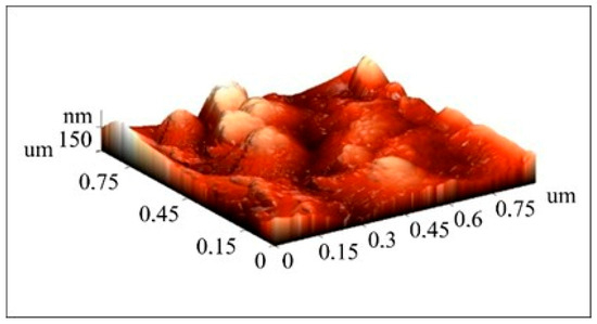
Figure 7.
AFM images of silicon film thickness—150 nm.
After reaching a given film thickness, in all experiments a sharp increase in the rate of growth of film thickness is observed. Atomic force microscopy was used to determine the surface morphology and the degree of uniformity of the deposition. The surface with different modifications of silicon has a large roughness. Semi-contact and contact AFM methods were used. Three-dimensional AFM images are also presented.
To assess the uniformity of the film thickness, the 3D model of the AFM image was analyzed using multiple sections. For each experiment, we obtained a data array of film thickness at different points on the sample. We processed the data arrays using statistical analysis methods. In this case, we obtained variances and standard deviations. Table 2 presents examples of the results of statistical analysis of data arrays, based on which it was concluded that the statistical indicators of the distribution of the film thickness over the substrate surface come to a minimum and stabilize with an increase in the median film thickness to 100–150 nm. The table does not present all the studied data arrays but only selected arrays to give an idea of the existing trends on which we relied in further analysis of the results.
Table 2.
Statistical parameters of data arrays of silicon film thickness values.
The data we obtained are consistent with the data of other studies. In particular, in the work of R. Edrei et al. [10], significant non-uniformity of the substrate coating is observed at a silicon film thickness of less than 150 nm (60–80 nm). Just like us, the authors used the method of sections of a three-dimensional AFM image model to estimate the non-uniformity of the film. However, unlike our work, this study did not find a film thickness above which the film is leveled and the roughness is reduced. As can be seen from Figure 8 [10], the condensed phase of silicon tends to grow in the vertical direction, perpendicular to the substrate. In contrast to these data, we found that with an increase in the film thickness of more than 100–150 nm, the film thickness is leveled over the entire surface of the substrate.
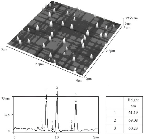
Figure 8.
Three-dimensional non-contact AFM image and its cross-section for amorphous silicon deposited at 560 °C [10].
However, the time it takes to achieve such a film thickness varies. The higher the specific power, the less time is needed to create a morphologically uniform film, i.e., the shorter the induction period of magnetron sputtering. Graphs of the dependence of the main indicators of magnetron sputtering, such as the induction period time, the film growth rate in stationary mode and silicon removal on the specific power at a constant (not pulsed) voltage on the target, the corresponding mathematical models and the approximation reliability values are presented in Figure 9, Figure 10 and Figure 11.

Figure 9.
Influence of specific power on film growth rate during magnetron sputtering at a constant voltage on the target.
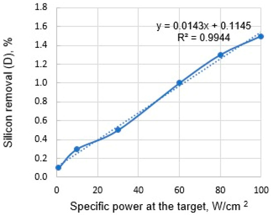
Figure 10.
Effect of specific power on silicon removal during magnetron sputtering at a constant voltage on the target.

Figure 11.
The influence of specific power on the induction period time in magnetron sputtering at constant voltage on the target.
Figure 9 shows a nonlinear graph of the dependence of the growth rate of the silicon film thickness obtained by magnetron sputtering on the specific power supplied to the crystalline silicon target. The film growth rate increases nonlinearly with increasing specific power. In the initial section, the curve has a steeper rise, then the growth rate slows down and reaches a plateau. Such behavior is typical and is explained by an increase in the flux of sputtered atoms with increasing power. The graph has a clearly defined maximum, which indicates the existence of an optimal value of the specific power at which the film growth rate is maximum. This is due to the fact that at too low a power, the flux of sputtered atoms is insufficient to ensure a high growth rate.
Figure 10 shows a graph displaying the dependence of the percentage of silicon removal (D) on the specific power supplied to the target during magnetron sputtering. The graph demonstrates a virtually linear relationship between the percentage of silicon removal and the specific power. This means that with increasing power supplied to the target, the amount of material that is sputtered and carried away from the system increases proportionally. At higher power, the number of ions bombarding the target increases, which leads to more intense knocking out of silicon atoms from the target surface. The value of the determination coefficient R2 is close to unity (R2 = 0.9944), which indicates a high degree of correlation between the experimental data and the approximating straight line. This indicates good approximation accuracy and reliability of the obtained results. The graph (Figure 11) demonstrates an exponential dependence of the induction period time on the specific power. This means that with increasing power supplied to the target, the time required for the start of stable film growth exponentially decreases. The value of the determination coefficient R2 indicates good approximation accuracy and reliability of the obtained results. The induction period time is the time required for the formation of a stable layer of atoms on the substrate surface and the start of continuous film growth. Increasing the power leads to an increase in the flow of sputtered atoms, which accelerates the process of nucleation and film growth. Consequently, the induction period time decreases. The exponential nature of the dependence is explained by the fact that the rate of nucleation is proportional to a certain degree of concentration of atoms on the substrate surface. With increasing power, the concentration of atoms increases rapidly, which leads to a rapid increase in the rate of nucleation and a reduction in the induction period time.
Summarizing the results presented in Figure 8, Figure 9 and Figure 10, the decrease in the most important indicator; the induction period time slows down to a range of 0.5–2.0 min, which corresponds to a specific power on the target of 60–100 W/cm2. In this case, the indicator—the rate of growth of the thickness of the silicon film also slows down in the region of 400–500 nm/min, and the removal (losses) of silicon monotonically increases as the specific power on the target increases. It can be assumed that with increasing power the flow of sputtered atoms increases, which leads to an increase in the film growth rate. However, high power values have a negative effect on the quality of the film, worsening its morphological characteristics. In addition, the obtained data can be used to model the sputtering process and predict the properties of the resulting films.
There are similar studies that examined the effect of the power supplied to the target on the magnetron sputtering rate [11]. In this work, sputtering was performed not with silicon but with copper on the surface of a glass substrate. In addition, the work provides absolute power values, not those reduced to the area of the target’s working surface. The geometric parameters of the target are also not specified. All this does not allow us to quantitatively compare their results with the results of our experiments. However, a similar trend can be noted. In the study [11], it was found that the growth rate increases exponentially with an increase in the power supplied to the target. In this case, the rate was increased by two orders of magnitude (up to 700 nm/s) compared to normal values under similar conditions at lower power (up to 5 nm/s). In our case, we also observe a significant increase in the sputtering rate, but the trend follows a power law rather than an exponential growth, eventually leveling off at a plateau.
Effect of the frequency of the voltage applied to the target on the main parameters of magnetron sputtering of silicon films. In order to study the possibility of further reduction in the induction period, similar experiments were carried out, during which the frequency of the voltage supplied to the target varied from 20 to 500 kHz.
Figure 12 shows a graph of the nonlinear dependence of the film thickness growth rate in the steady-state mode on the frequency of the voltage supplied to the target during magnetron sputtering. In the initial section, the curve has a steeper rise, then the rate growth slows down and reaches a plateau. The graph has a maximum, which indicates the existence of an optimal voltage frequency value at which the film growth rate is maximum. This is due to the fact that at too low a frequency, the flux of sputtered atoms is insufficient to ensure a high growth rate, and at too high a frequency, various negative effects may occur, such as overheating of the target, a change in the plasma composition, and deterioration of the adhesion of the film to the substrate. With increasing frequency, the power supplied to the discharge increases, which leads to an increase in the flux of sputtered atoms and, consequently, to an increase in the film growth rate.
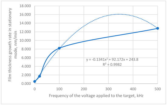
Figure 12.
Graph of the dependence of the film thickness growth rate on the frequency of the voltage supplied to the target during magnetron sputtering at a constant specific power on the target—100 W/cm2.
The graph (Figure 13) shows the dependence of the percentage of silicon removal (D) on the frequency of the voltage supplied to the target during magnetron sputtering. The percentage of silicon removal increases nonlinearly with increasing voltage frequency. At the initial section, the curve has a steeper rise, then the rate growth slows down and reaches a plateau and is explained by the increase in the flow of sputtered atoms with increasing frequency. The graph has a clearly defined maximum, which indicates the existence of an optimal value of the voltage frequency, at which the percentage of silicon removal is maximum. This is due to the fact that at too low a frequency, the flow of sputtered atoms is insufficient to ensure a high removal rate, and at too high a frequency, various negative effects may occur, such as overheating of the target, a change in the plasma composition, and deterioration of the adhesion of the film to the substrate.
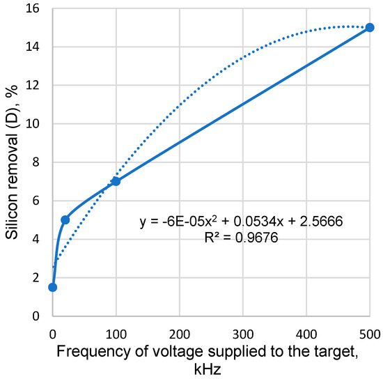
Figure 13.
Graph of the dependence of the percentage of silicon removal (D) on the frequency of the voltage supplied to the target during magnetron sputtering at a constant specific power on the target—100 W/cm2.
The graph (Figure 14) displays the exponential dependence of the induction period time on the voltage frequency supplied to the target during magnetron sputtering of silicon. An increase in the voltage frequency leads to a rapid increase in the concentration of atoms, which leads to a rapid increase in the rate of nucleation and a reduction in the induction period time. As can be seen from the graph (Figure 13), it makes sense to study the magnetron sputtering process in a wider range of voltage frequencies. In the frequency range from 100 to 500 kHz, the reduction in the induction period time is not as significant as in the range from 0 to 100 kHz. It is obvious that the graph has not yet fully reached a plateau and there is significant potential for further intensification of the magnetron sputtering process. However, in this work we were limited by the capabilities of the equipment we have. In further studies, we will look for opportunities to increase the frequency of magnetron sputtering voltage, and we also recommend that researchers who will work in this direction keep this in mind.

Figure 14.
Graph of the dependence of the induction period time on the frequency of voltage supplied to the target during magnetron sputtering at a constant specific power on the target—100 W/cm2.
Increasing the voltage frequency on the target, on the one hand, increases the productivity of the magnetron sputtering process, but on the other hand, we lose silicon with the gas leaving the working chamber. Therefore, it is necessary to seek a compromise in this regard. The optimization strategy should then be of an economic nature and concern not only the process of obtaining anode films but the finished product—a lithium-ion battery (LIB). In the process of industrial optimization of the process, we observe how the specific consumption of electrical energy and the cost of the wages of the plant operator will change with an increase in the voltage frequency. Since productivity increases with an increase in the frequency, the time of manufacturing the LIB will decrease. The power of the sputtering plant is constant, regardless of the frequency. Therefore, reducing the time of manufacturing the LIB will reduce the energy costs for the manufacture of a unit of LIB power. Similarly, for the costs of the wages of the magnetron sputtering plant operator. Since silicon carryover increases with an increase in the voltage frequency, the specific consumption of silicon for manufacturing the LIB increases accordingly. We transform the mass specific consumption of silicon into financial costs. We sum up the costs of electricity, wages, and silicon. To do this, we will need data on the cost of the above resources at the enterprise that will commercialize the technology. We ensure that in each case the technical characteristics of the LIB remain at the same level and the magnetron sputtering equipment operates stably in a safe mode. We plot a graph of the dependence of total costs on the voltage frequency. Perhaps this graph will have a minimum, since at some point the positive effect of increased productivity will be offset by the negative effect of increased specific silicon consumption. It is possible that the minimum will not be reached due to technical limitations of the equipment in terms of voltage frequency or due to deterioration in the quality of the LIB when a certain voltage frequency level is exceeded. In this work, we do not carry out such optimization, but we plan to as our project develops.
An increase in frequency is traditionally associated with a decrease in the ion energy distribution (IED) width. In turn, a narrow IED width promotes a more uniform deposition of material on the substrate and a decrease in the deposition rate. In this sense, we have obtained a result that is not quite traditionally expected. Probably, this is due to the fact that we accompanied the increase in voltage frequency with a fairly high-power density on the target. The result was an inversion of traditional trends, when an increase in frequency at high powers, although insignificant, reduces the film quality and an ultra-high deposition rate is achieved. Unfortunately, we cannot use this effect in practice, since the rate increase is achieved at too large a film thickness beyond the induction period time limit. The paradoxical nature of the obtained result could be explained if we studied the experimental ion bombardment spectra. However, unfortunately, our magnetron equipment was not equipped with a differentially pumped delay grating analyzer of the ion flux energy. We hope that colleagues who have such an opportunity will repeat our study and will be able to explain the effect we obtained. In this regard, we propose here a preliminary working hypothesis to explain this effect. As the voltage frequency and specific power applied to the target increase, the ions acquire higher energy, which increases the efficiency of sputtering the material from the target. This leads to a larger number of sputtered silicon atoms that pass into the gas phase, resulting in increased losses.
3. Materials and Methods
To conduct experimental studies, the most productive of the currently existing equipment options was chosen—the Caroline D12C system. The Caroline D12C vacuum deposition system is intended for small- and medium-scale production and research in the field of thin-film deposition using magnetron and thermal sputtering.
When choosing the temperature and environmental conditions for the initial study, we decided to limit ourselves to standard operating conditions of the magnetron sputtering equipment, since in this case the research results will be easier to implement in the actual production process.
Silicon crystals were used as targets for magnetron sputtering. To produce silicon crystals, we used TCR-5C-1k/t equipment, manufactured by Techno Search Corporation (Tokyo, Japan). The crystals were grown according to the Czochralski method using commercial high-purity silicon of SoG-Si grade 6–7 N. The silicon melt was previously exposed to a vacuum, which also made it possible to minimize the amount of impurities in the silicon powder. Silicon powder was loaded into a crucible made of high-purity quartz with a diameter of 5 cm and a height of 7 cm. The crucible was installed in the graphite element of the heating part of the system in the middle position. In the graphite element, the crucible was heated to 1500 °C for 2 h in an inert atmosphere. Argon was used as an inert gas. In this way, uniform heating of the powder was achieved. The initial silicon crystal (seed) in the form of a round rod with a diameter of 3 mm was fixed in a holder. Using a tungsten wire, the seed was lowered into the crucible until it came into contact with the surface of the melt. The seed attracts crystallizing silicon particles from the melt. In this way, a silicon crystal is formed. Samples were prepared from silicon crystals for subsequent magnetron sputtering. The sample preparation includes the following steps:
- -
- cutting the crystal with a diamond disk into cylindrical samples;
- -
- grinding the cylindrical samples with abrasive micropowders;
- -
- polishing the samples using synthetic diamond micropowders of grades ASM7–ASM1, with a grain size from 7 microns to 1 micron and finer.
The substrate was a copper foil 0.5 mm thick, with varying degrees of difference (roughness), which was pre-etched with an alcohol solution of ammonia. Before deposition, the copper foil was sanded with sandpaper with an average grain size of 200 μm.
The substrate material can significantly affect the magnetron sputtering process. For example, the ability of ionized silicon to deposit from the plasma flow onto the substrate and the features of the growth of colonies of condensed silicon in the horizontal and vertical directions. However, we are significantly limited in the choice of substrate material when considering its application for LIB. The substrate must have good electrical conductivity, and copper or aluminum are the most suitable options. Since aluminum has lower electrical conductivity, we primarily focused on studying the deposition of silicon on a copper substrate.
A preliminary assessment of the film morphology was carried out using the ELLIPS-1891 spectral ellipsometer (ELLIPS, Eindhoven, The Netherlands), designed for precision measurements of the thickness of thin films, the optical parameters of thin-film structures and the spectral dependences of the optical constants of the surfaces of various materials (metals, semiconductors, dielectrics, etc.). When the uniform morphology of the silicon film was revealed and the absence of a substrate surface not covered by the film, further determination of the thickness of the resulting film was carried out using a Jeol scanning electron microscope JSM-6490 LA (JEOL, Tokyo, Japan), with a magnification range of up to 300,000×.
The most important parameter of the silicon nanofilm formation process is the specific power at the target. Obviously, an increase in power will accelerate the ionization of target silicon atoms and their transition into plasma. Accordingly, a greater flow of silicon in the direction of the substrate will provide a greater speed of film growth. In this regard, the specific power during magnetron sputtering was varied in the maximum possible range from 1 to 100 W/cm2, taking into account the available technical capabilities of the modern production equipment.
The second important indicator is the working pressure in the working chamber. After a deep vacuum is created in the working chamber and voltage is applied to the target, an inert gas is supplied to the chamber, which is a means of transporting ionized silicon to the surface of the substrate. By adjusting the amount of supplied inert gas, the operating pressure in the chamber is regulated. For the existing industrial equipment, the pressure control range is from 0.5 to 3.0 Pa. An increase in gas flow (increase in operating pressure) accelerates film growth. However, on the other hand, an excessive increase in gas velocity in the working chamber can affect the loss of silicon along with the gases leaving the chamber. Therefore, in all experiments, silicon removal during the deposition process was monitored. Silicon removal (D) was estimated as the ratio of the difference in target weight loss and the increase in the weight of the resulting film to the target weight loss according to Formula (1).
where —is the target weight loss during magnetron sputtering, g.
—increase in the weight of the film obtained in the process of magnetron sputtering, g.
The third important parameter of magnetron sputtering is the frequency of the voltage pulses applied to the target. Presumably, an increase in the frequency of impact on the target will accelerate the destabilization of the atomic lattice, the ionization of silicon atoms, and their transition into plasma. In this regard, three voltage pulse frequency levels available during the experiments were used—20, 100, and 500 kHz.
4. Conclusions
The research established that the process of magnetron sputtering of silicon qualification grade 6–7 N is characterized by an induction period. The boundary of this induction period is determined by the thickness of the film, which reaches 100 nm. Up to this thickness, the morphology of the film is non-uniform. The density of particle formation on the substrate is uneven, with particle agglomerations occurring. Some areas of the substrate do not contain silicon particles. The conventional rate of film formation in this period is 5 nm/min, with a minimum specific power on the target of 1 W/cm2 and a constant voltage applied to the target. After the formation of a continuous film surface, the growth rate of the film thickness increases sharply to 35–40 nm/min. The kinetic curves of film thickness growth in stationary mode are exponential for low (0.5–1.5 Pa) and high (3.0 Pa) pressures, and linear for the middle range (2.0–2.5 Pa).
Based on scanning electron microscopy data, it was found that all the films demonstrated the presence of a porous structure, expressed to varying degrees. At low pressures (0.5–1.0 Pa), a denser film with fewer pores is formed. With increasing pressure (2.0–3.0 Pa), the film becomes increasingly porous, with a pronounced colonial structure and a rough surface. Increasing the pressure to 3.0 Pa leads to deterioration of the morphological characteristics of the film and a decrease in its quality. An operating gas pressure of 2 Pa is preferable, since the film obtained at such a pressure shows the presence of pores uniform in size and distribution. This should ensure long-term stability of the film when the anode is saturated with lithium ions in the charge–discharge cycle of the LIB.
An increase in the specific power supplied to the target in the variation range of 1 to 100 W/cm2 reduces the induction period from 20 to 0.5 min and increases the film growth rate in stationary mode from 35 to 40 to 500 nm/min at a constant voltage applied to the targets. Silicon losses are insignificant at the level of 0.5–1.5% over the entire range of specific powers studied. However, when using an alternating voltage on the target, a maximum specific power of 100 W/cm2 and an increase in the frequency of voltage pulses to 20–500 kHz, silicon losses increase to 7–15% with a sharp reduction in the induction period to 5–15 s and an increase in the growth rate of silicon films up to 12800 nm/min in stationary mode. Unfortunately, such speeds are achieved after the induction period, when the thickness of the silicon film is already several micrometers. Such a large film thickness is unacceptable for us. Therefore, the actual speeds when scaling the process will be much less than 500–1000 nm/min, in order to complete the process by the time the film thickness is 100–150 nm. The obtained result can significantly increase equipment productivity when organizing the production of silicon anodes for lithium-ion batteries (LIB) using the magnetron sputtering method.
Author Contributions
All authors contributed to the study conception and design. Material preparation and methodology were developed by B.Z.; data collection and analysis were performed by K.T. (Figure 1), N.Z. (Figure 6, Figure 7, Figure 8, Figure 9, Figure 10 and Figure 11), and G.D. (Figure 2, Figure 3, Figure 4 and Figure 5). The first draft of the manuscript was written by K.T. and S.K. All authors commented on previous versions of the manuscript. All authors have read and agreed to the published version of the manuscript.
Funding
This research received no external funding.
Data Availability Statement
Data are available upon request to the author.
Conflicts of Interest
The author declare no conflicts of interest.
References
- Mikhailova, T.S.; Kalusulingam, R.; Bogush, I.Y.; Myasoedova, T.N. Impedance sensors based on silicon-carbon films for detection low concentrations of organic vapors. Solid-State Electron. 2024, 220, 108978. [Google Scholar] [CrossRef]
- Catchpole, K.R.; McCann, M.J.; Weber, K.J.; Blakers, A.W. A review of thin-film crystalline silicon for solar cell applications. Part 1: Native substrates. Sol. Energy Mater. Sol. Cells 2001, 68, 173–215. [Google Scholar] [CrossRef]
- Hamakawa, Y. Solar PV energy conversion and the 21st century’s civilization. Sol. Energy Mater. Sol. Cells 2002, 74, 13. [Google Scholar] [CrossRef]
- Bergmann, R.B.; Werner, J.H. The future of crystalline silicon films on foreign substrates. Thin Solid Film. 2002, 162, 403–404. [Google Scholar] [CrossRef]
- Chan, C.K.; Peng, H.; Liu, G.; McIlwrath, K.; Zhang, X.F.; Huggins, R.A.; Cui, Y. High-performance lithium battery anodes using silicon nanowires. Nat. Nanotechnol. 2008, 3, 31–35. [Google Scholar] [CrossRef] [PubMed]
- Yao, W.; Zou, P.; Wang, M.; Zhan, H.; Kang, F.; Yang, C.H. Design Principle, Optimization Strategies, and Future Perspectives of Anode-Free Configurations for High-Energy Rechargeable Metal Batteries. Electrochem. Energy Rev. 2021, 4, 601–631. [Google Scholar] [CrossRef]
- Berla, L.A.; Lee, S.W.; Cui, Y.; Nix, W.D. Mechanical behavior of electrochemically lithiated silicon. J. Power Sources 2015, 273, 41–51. [Google Scholar] [CrossRef]
- Limthongkul, P. Electrochemically-driven solid-state amorphization in lithium–metal anodes. J. Power Sources 2003, 119, 604–609. [Google Scholar] [CrossRef]
- Zhautikov, B.A.; Zobnin, N.N.; Romanov, V.I.; Aikeeva, A.A.; Zhautikov, F.B.; Dairbekova, G.S.; Zhaslan, R.K. Patent 34959 Republic of Kazakhstan, IPC N01M 10/02. Lithium-Ion Battery Pack. Applicant and Patent Holder: RSE on PVC “KGIU”; publ. 03/19/2021, Bulletin. No. 11.7p. Available online: https://gosreestr.kazpatent.kz/Invention/Details?docNumber=317309 (accessed on 11 March 2025).
- Edrei, R.; Shauly, E.N.; Roizin, Y.; Hoffman, A. The effect of deposition process parameters and post-deposition treatments on the poly- and amorphous-silicon morphology. Appl. Surf. Sci. 2022, 188, 539–544. [Google Scholar] [CrossRef]
- Krivobokov, V.P.; Yanin, S.N.; Tretyakov, R.S. High-Speed Magnetron Deposition of Metallic Coatings//Reshetnevskie Readings. 2010. No. 14. Available online: https://cyberleninka.ru/article/n/vysokoskorostnoe-magnetronnoe-osazhdenie-metallicheskih-pokrytiy (accessed on 9 March 2025).
Disclaimer/Publisher’s Note: The statements, opinions and data contained in all publications are solely those of the individual author(s) and contributor(s) and not of MDPI and/or the editor(s). MDPI and/or the editor(s) disclaim responsibility for any injury to people or property resulting from any ideas, methods, instructions or products referred to in the content. |
© 2025 by the authors. Licensee MDPI, Basel, Switzerland. This article is an open access article distributed under the terms and conditions of the Creative Commons Attribution (CC BY) license (https://creativecommons.org/licenses/by/4.0/).