Article

Early Stage of Sb Ultra-Thin Film Growth: Crystal Structure and Electron Band Structure

by
Mirosław Stróżak
,
Marek Kopciuszyński
,
Agnieszka Stępniak-Dybala
,
Mariusz Krawiec
and
Mieczysław Jałochowski
*
Institute of Physics, Maria Curie-Skłodowska University, Pl. M. Curie-Skłodowskiej 1, 20-031 Lublin, Poland
*
Author to whom correspondence should be addressed.
Condens. Matter 2016, 1(1), 11; https://doi.org/10.3390/condmat1010011
Submission received: 10 November 2016 / Revised: 8 December 2016 / Accepted: 14 December 2016 / Published: 16 December 2016

Abstract

:
The evolution of the electron band structure upon the reduction of Sb film on a Si(111)-(6 × 6)Au substrate, relevant to topological insulator properties, is experimentally systematically investigated by the reflection high-energy electron diffraction (RHEED), in situ surface electron transport and angular resolved photoemission spectroscopy methods. The experiments reveal that a bilayer (BL) of Sb is crystalline but the subsequent three BLs on top of it form amorphous layers. The five-BL-thick film transforms back to the crystalline form. The bilayer as well as 1.2- and 3.8-BL-thick films show the electron band structure with a relatively large energy gap at the Γ point of the Brillouin zone. The theoretically predicted band structure is observed at 4.8 BL coverage.

1. Introduction

Two surface bands of elemental antimony are connected to the conduction band and the valence band separately. According to the theory, ultra-thin, four- to seven-bilayer (BL)-thick Sb(111) films should be topologically nontrivial [1]. However, the electronic structure features a small negative band gap which avoids the existence of a topologically invariant phase [2]. Although the bulk antimony crystal is semi-metallic, it is believed that in the form of ultra-thin film, it should acquire topological insulator properties [3]. First-principles calculations suggest that the topologically nontrivial insulating phase can be induced by tensile strain, pointing to the possibility of realizing the quantum Hall state for Sb thin films on proper substrates [4]. On the other hand, the reduction of the film thickness leads to the increase of the coupling between opposite surface states, and thus to the degradation or even destruction of novel properties. Moreover, due to a high surface-to-volume ratio, the band structure of ultrathin Sb films should be sensitive to surface reconstruction, interface and substrate electronic structures and substrate morphology [1]. Thus, it should be possible to modify the band structure of Sb films by its interaction with various substrates.
The first-principles calculations have predicted the surface-coupling–induced gap in four and five-BL films [5]. Another theoretical work [6] has also studied this problem and came to similar conclusions, i.e., the free-standing ultra-thin Sb films with a preserved, although relaxed, crystal structure should undergo the transition from a simple wide-band-gap material (one BL thick) to a topological insulator phase for films with thicknesses between four and eight BLs, and then to ordinary semi-metal. However, real ultra-thin systems always interact with a substrate and the resulting crystal structure modifications will certainly influence the Sb band structure.
In the present paper we report on the reflection high-energy electron diffraction (RHEED), the angular resolved photoemission electron spectroscopy (ARPES), and the in situ electric surface resistance variation study of Sb films on the Si(111)-(6 × 6)Au surface. We show that the electronic structure of 1.2 BL crystalline Sb film features a relatively large energy gap, which exists also in 1.2- to four-BL-thick partially amorphous films. At room temperature, 4.8-BL-thick film transforms spontaneously into the crystalline phase with the electron band structure characteristics of Sb crystalline ultra-thin films. The observed modifications of the band structure of Sb(111) support existing theoretical predictions [3,4,5,6].

2. Methods and Parameters

The measurements were performed at room temperature (RT) in separate UHV chambers with the base pressure around 7 × 10⁻¹¹ mbar. The n-type Si(111) samples, with dimensions of 18 × 4 × 0.4 mm3 and specific resistivity of 26 ÷ 33 Ω·cm, were used in experiments. The Si(111)-(6 × 6)Au surface reconstruction was prepared by deposition of 1.4 monoatomic layers (expressed in units equivalent to one half of Si(111) surface atoms density) of Au and subsequent annealing [7,8]. The Si(111)-(6 × 6)Au surface features the flat topography, metallic character of the bands, and large surface energy—a favorable property allowing to grow macroscopically flat two dimensional (2D) structures exhibiting pronounced quantum size effects (QSE) [7].
The electrical resistance was determined in situ by measuring the voltage drop V between two tungsten electrochemically etched tips placed on the Si(111) surface exposed to evaporators. Two Mo clamps at the sample edges served as contacts for the current. During Sb deposition 2 μA AC (alternating current) 1025 Hz stabilized current was applied to the sample clamps and a voltage signal from the pair of tungsten tips was detected by the lock-in amplifier. The method was successfully used previously in the electrical conductivity studies of metallic quantum wells on Si(111) [7] and Pb atomic chains on Si(553)-Au surface [9]. Sb was deposited on the Si(111)-(6 × 6)Au substrate at the rate of about 0.3 BL/min. measured with a quartz crystal microbalance with accuracy better than ±15%. One BL of Sb(111) counts 12.43 × 10¹⁴ atoms/cm2.
The ARPES measurements were performed in a separate UHV chamber equipped with a high intense He lamp (He I line, = 21.2 eV) and a hemispherical electron energy analyzer (Phoibos 150) (SPECS, Berlin, Germany) with the 2D MCP detector and 12 bit CCD camera. The energy resolution was set to 40 meV. The crystal structure of a substrate and the growing Sb film were monitored by the RHEED (home-made, Lublin, Poland).

3. Results and Discussion

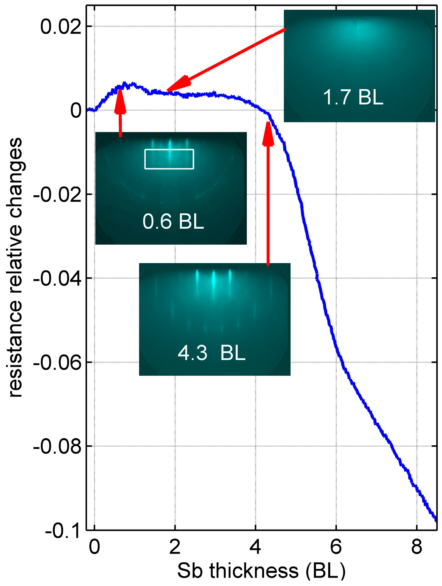
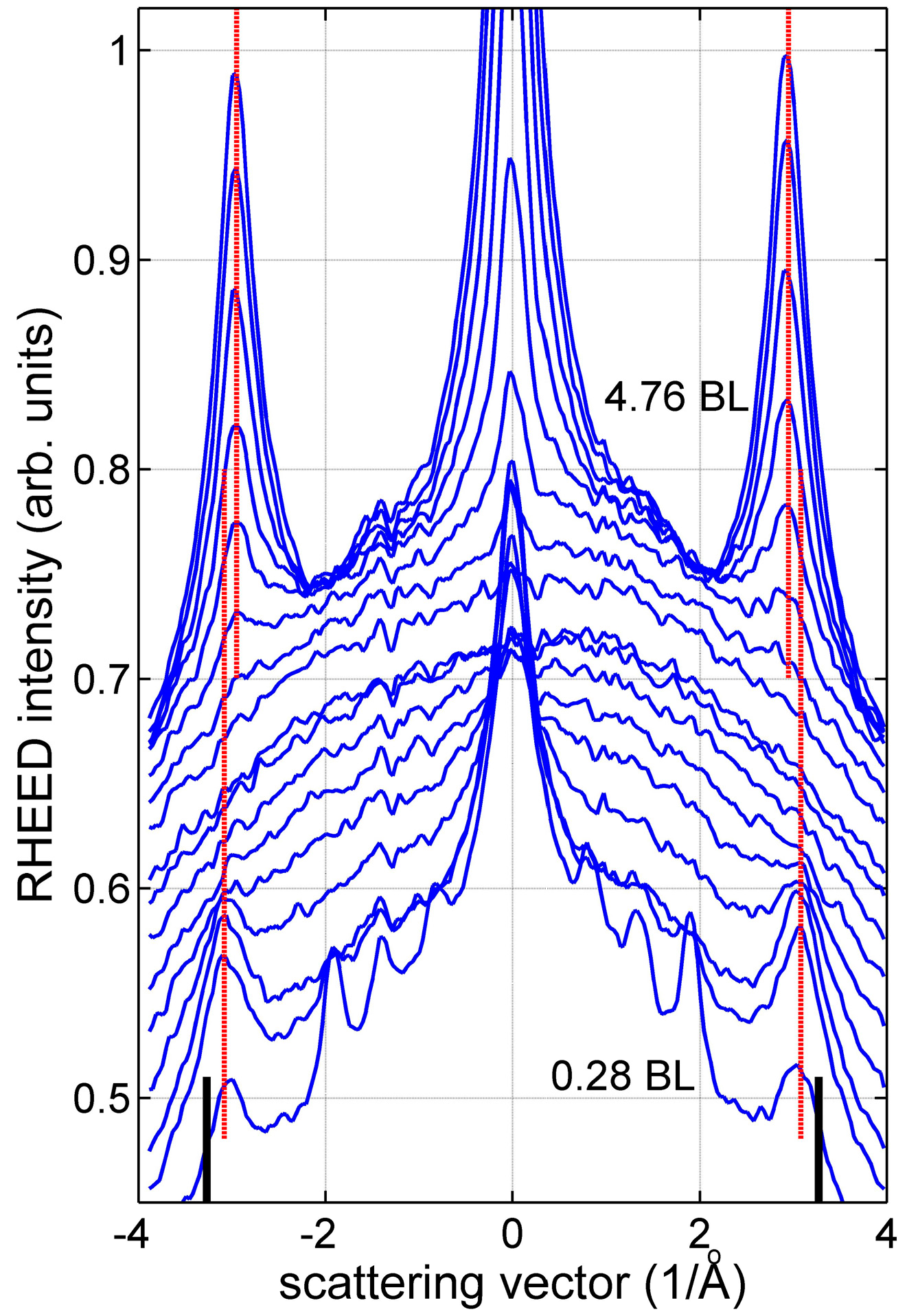
3.1. Crystal Structure and Electric Transport of Sb Layers Grown on Si(111)-(6 × 6)Au

Figure 1 displays selected in situ electron diffraction patterns and surface resistance–relative variations, recorded simultaneously during the Sb deposition. The patterns are characterized by three distinct Sb crystal structure phases. Phase I consists of an (111) epitaxial layer in plane orientation, the same as the substrate. The RHEED pattern of 0.6-BL-thick film in the middle of Figure 1 shows the crystalline order. For films deposited at room temperature, phase II spans from about 1.2 BL to about 4.5 BL. As is evident from the RHEED pattern shown in Figure 1, the 1.7-BL-thick film is already completely amorphous. Further film deposition results in the spontaneous transition of this structure into the crystalline phase, similar to phase I. The obtained phase remains stable upon further deposition of Sb. Both crystal structure transformations are relatively sharp and occur within about a 0.2–0.5 BL thickness range. At lower temperatures phase II widens and eventually starts from the beginning of the film growth. On the other hand, phase II shrinks during growth above the RT. Moreover, for a sufficiently high temperature, around 500 K, phase III forms three-dimensional islands.
The evolution of the Sb film crystal structure is also reflected in the in situ surface resistance variations, shown in Figure 1. The plot shows that in phase I, the film surface resistance slightly increases, forming a small “bump” with a maximum at 0.8 BL. In the case of 1.2 BL, where phase II appears, the resistance stabilizes and remains almost constant up to about 3.5 to four BLs, which corresponds exactly to the thickness of phase II observed by RHEED. Phase III starts with a rapid drop of the surface resistance, which decreases further as a function of the coverage. Moreover, it is possible to distinguish two regions with different slopes of the linearly decreasing resistance.
It is well known that the electric transport in the Si(111)-(6 × 6)Au is mediated by the metallic surface, not by the space charge layer [10]. Therefore, this system is sensitive mainly to the surface scattering and not to a possible doping caused by arriving atoms. These facts allow us to explain the origin and the shape of the resistance “bump”. During the Sb deposition, the arriving atoms act as scattering centers, hindering the electron transport. The effect reaches its maximum before the first BL is completed, i.e., when the layer is extremely rough. This also explains why the resistivity remains constant in phase II. Apparently, the amorphous layer formed on top of the first BL neither introduces additional charge carriers nor changes the electron scattering at the interface. The corresponding RHEED patterns show that phase III forms a well-ordered crystal already at 4.5 BLs. However, the change of the surface resistance curve slope at six BLs suggests that this process continues until six BLs.
Phases I and III, although both crystalline, differ in their lattice constants. A close inspection of the position of the RHEED pattern streaks as a function of the deposited Sb thickness allows us to determine the lattice constant for first BL and for a thickness greater than three BLs. Figure 2 shows a set of RHEED intensity profiles obtained from the pattern area outlined in the middle inset of Figure 1.
The positions of the peaks associated with the Si(111)-(6 × 6)Au surface allow us to precisely determine the Sb (111) surface lattice constant. They yield 4.10 ± 0.05 Å for phase I, and 4.27 ± 0.05 Å for phase III, respectively. These values can be compared to the bulk parameter equal to 4.31 Å [11] and to the theoretically optimized lattice constant for a free-standing single BL equal to 4.12 Å [6]. Similarly, for three BL and four BL films, the theoretical lattice constants are equal to 4.29 Å and 4.32 Å, respectively. All the above theoretical lattice constant parameters fit the experimentally determined values in our studies well.

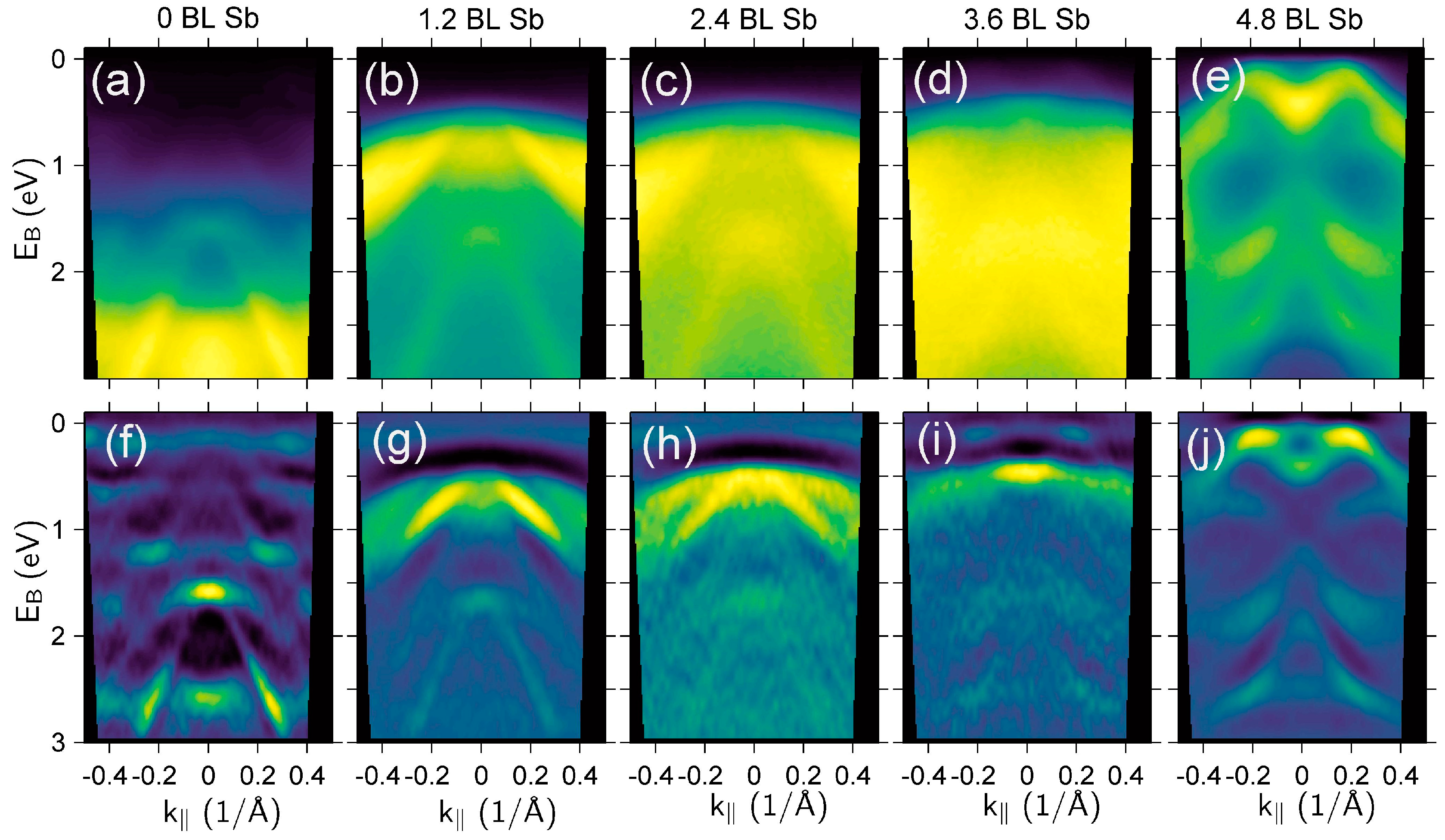
3.2. Electron Band Structure of Ultra-Thin Sb Films

Figure 3 shows the ARPES intensity maps (top row) and the corresponding second derivative (bottom row) of the bare and Sb-covered Si(111)-(6 × 6)Au substrate measured along the antimony surface Brillouin zone (BZ) K-Γ-K line. Obviously, the observed evolution of the energy bands is related to the crystalline structure of the samples. The amorphous structure of 2.4 BL- and 3.6-BL-thick films observed in RHEED may suggest the lack of any well-developed electron band, but this is not the case. We can see in Figure 3h,i the pairs of bands with top edges located at 0.54 eV and 0.52 eV below the Fermi level, respectively, for samples 2.4 BLs and 3.6 BLs thick. The band with a lower dispersion can be identified as the surface states located in the bulk gap [6]. Apparently, the layers feature some crystal order, not detected by the RHEED measurements.
In order to explain this discrepancy, we compare photoemission maps for 1.2 BLs, shown in Figure 3b,g, and 2.4 BLs, shown in Figure 3c,h. Both maps show the same bands, with the same dispersion and with almost the same energy. The main difference, in particular between maps in Figure 3g,h, is the noisy photoemission intensity in Figure 3h uniformly superimposed on the well-developed band structure in Figure 3g. Therefore, it is reasonable to assume that deposition of the second, the third, and the fourth layer of Sb preserves the crystal structure with the electron bands displayed in Figure 3b,g. Indeed, phase II, as observed in the RHEED and in the resistance data, is not uniform inside, crystalline at the interface and amorphous on the top. After the crystal structure transformation into phase III, the electron energy band structure, shown in Figure 3e,j, changes dramatically—new bands appear at the Fermi energy—and the surface band, seen in Figure 3j at the Γ-point near the Fermi energy, moves up. The figure shows that a second surface band emerges just below the Fermi level at the Γ-point. This finding confirms the theoretical prediction of such an electron band structure configuration expected for Sb five-BL-thick films [3].
Considering the electron band structure of 1.2 BL Sb thin film, it is worthwhile to mention the exceptional stability of this buried layer. As it was recently pointed out [12], a buckled honeycomb structure with a 2D hexagonal lattice can be a candidate for a stable structure. Unlike in the case of graphene and silicene, which have unsaturated metallic bonds, the one-BL-thick hexagonal Sb structure features saturated bonds. This theoretical result suggests that the one BL Sb interacts weakly with the substrate and with the second BL growing on the top of it, thus making it prone to forming an amorphous phase as observed in our experiments.

4. Conclusions

In conclusion, we have studied the thickness-dependent crystal structure, electron transport and electron band structure of Sb films within the thickness range of one to five BLs deposited on a Si(111)-(6 × 6)Au substrate. We have found that the single BL film (phase I) grows in a crystalline manner and preserves its crystallinity upon the deposition of the next three amorphous BLs (phase II). The entire film transforms into the crystalline phase after reaching the thickness of five BLs (phase III). The proposed model of the film growth was supported by results of in situ surface resistance measurements. This was further confirmed by the ARPES data. Experimental photoemission spectra of 2.4- and 3.6-BL-thick films were very similar to that of single BL. Indeed, the second, third, and fourth BLs grown on top of the first layer are electronically “dead” and do not contribute either to the electron band structure or to the surface electron transport. These films are insulators with relatively large energy gaps at the Γ-point of the Brillouin zone. Further, 4.8-BL-thick crystalline film surface bands located at the energy gap have been detected at the Γ-point. Our findings deliver clear evidence that 4.8-BL-thick Sb film on a Si(111)-(6 × 6)Au substrate fulfills some of the theoretically predicted criteria of the two-dimensional topological insulator [3]—a small energy gap and two surface states at the Γ-point. However, we point out that this conclusion is limited only to the Sb lattice reciprocal space around the Γ-point.
Part of this work has been presented at the international conference on Atomically Controlled Surfaces, Interfaces and Nanostructures ACSIN2016 held in Frascati, Rome, Italy, on October 9–15, 2016 [13].

Acknowledgments

This work was supported by the National Science Center, Poland, under Grant No. 2014/13/B/ST5/04442.

Author Contributions

Mirosław Stróżak performed resistance in situ and RHEED measurements. Marek Kopciuszyński performed ARPES measurements. Agnieszka Stępniak-Dybala optimized ultra-thin Sb film growth. Mariusz Krawiec analyzed the data. Mieczysław Jałochowski wrote the manuscript. All authors have read and approved the final manuscript.

Conflicts of Interest

The authors declare no conflict of interest.

References

  1. Zhang, P.F.; Zheng, L.; Duan, W.; Liu, F.; Wu, J. Topological and electronic transitions in Sb(111) nanofilm: The interplay between quantum confinement and surface effect. Phys. Rev. B 2012, 85, 201410(R). [Google Scholar] [CrossRef]
  2. Fu, L.; Kane, C.L. Topological insulators with inversion symmetry. Phys. Rev. B 2007, 76, 045302. [Google Scholar] [CrossRef]
  3. Wang, S.-X.; Zhang, P.; Li, S.-S. Topological properties of Sb(111)surface: A density functional theory study. 2012; arXiv:1201.1976. [Google Scholar]
  4. Chuang, F.C.; Hsu, C.H.; Chen, C.-Y.; Huang, Z.-Q.; Ozolins, V.; Lin, H.; Bansil, A. Tunable topological electronic structures in Sb(111) bilayers: A first-principles study. Appl. Phys. Lett. 2013, 102, 022424. [Google Scholar] [CrossRef]
  5. Wang, D.; Chen, L.; Liu, H.; Wang, X. Topological phase transition in Sb(111)films driven by external strain and electric field. EPL 2013, 104, 57011. [Google Scholar] [CrossRef]
  6. Wang, D.; Chen, L.; Liu, H.; Wang, X.; Cui, G.; Zhang, P.; Zhao, D.; Ji, S. Topological states modulation of Bi and Sb thin films by atomic adsorption. Phys. Chem. Chem. Phys. 2015, 17, 3577–3583. [Google Scholar] [CrossRef] [PubMed]
  7. Jałochowski, M.; Bauer, E. Quantum size and Surface effects in the electrical resistivity and high-energy electron reflectivity of ultrathin lead films. Phys. Rev. B 1988, 38, 5272–5280. [Google Scholar] [CrossRef]
  8. Stępniak, A.; Nita, P.; Krawiec, M.; Jałochowski, M. In and Si adatoms on Si(111)5 × 2-Au: Scanning tunneling microscopy and first-principles density functional calculations. Phys. Rev. B 2009, 80, 125430. [Google Scholar] [CrossRef]
  9. Jałochowski, M.; Kwapiński, T.; Łukasik, P.; Nita, P.; Kopciuszyński, M. Correlation between morphology, electron band structure, and resistivity of Pb atomic chains on the Si(553)-Au surface. J. Phys. Condens. Matter 2016, 28, 284003. [Google Scholar] [CrossRef] [PubMed]
  10. Hasegawa, S.; Tong, X.; Takeda, S.; Sato, N.; Nagao, T. Structures and electronic transport on silicon Surfaces. Prog. Surf. Sci. 1999, 60, 89–257. [Google Scholar] [CrossRef]
  11. Barrett, C.S.; Cucka, P.; Haefner, K. The crystal Structure of Antimony at 4.2, 78 and 298 K. Acta Cryst. 1963, 16, 451–453. [Google Scholar] [CrossRef]
  12. Üzengi Akturk, O.; Ongun Özçelik, V.; Ciraci, S. Single-layer-crystalline phase of antimony: Antimonenes. Phys. Rev. B 2015, 91, 235446. [Google Scholar] [CrossRef]
  13. Bianconi, A.; Marcelli, A. (Eds.) Atomically Controlled Surfaces, Interfaces and Nanostructures; Superstripes Press: Rome, Italy, 2016; ISBN 9788866830597.
Figure 1. Surface resistance relative changes recorded during Sb deposition on Si(111)-(6 × 6)Au substrate at room temperature. Insets show three selected RHEED patterns at characteristic stages of Sb growth. Labels in the patterns and red arrows indicate corresponding film thicknesses. A rectangular shape in the RHEED pattern in the middle of the figure outlines the image area for further detailed analysis (Figure 2).
Condensedmatter 01 00011 g001
Figure 2. RHEED intensity profiles recorded during the Sb film growth at room temperature. Only the small area of patterns outlined in Figure 1 is taken for analysis. The curves are drawn for every 0.28 BL of Sb. Scattering vector is pointed along the <112> direction of the substrate and the Sb film. Two black bars placed at the bottom at ±3.27 (1/Å) denote peak positions expected for the Si(111) surface with the bulk lattice constant. Two sets of perpendicular red lines denote Sb peak positions for sample phase I (bottom) and phase III (upper). Well-resolved peaks within the scattering vector range ±2.0 (1/Å) for 0.28-BL-thick film (bottom) originate from the Si(111)-(6 × 6)Au reconstruction.
Condensedmatter 01 00011 g002
Figure 3. ARPES intensity spectra of the bare and Sb-covered Si(111)(6 × 6)Au surface measured along the Sb surface BZ K-Γ-K line (ae), and second derivative of the intensity (fj). The spectra were acquired at room temperature. (a,f) Bare Si(111)-(6 × 6)Au substrate. The Si upper valence band with the upper edge at the binding energy of 1.60 eV is visible. Some surface metallic states exist at the Fermi energy. In (bd) and (gi) an energy gap is observed for 1.2-, 2.4-, and 3.6-BL-thick Sb. Sb valence band edge is located at 0.54 ± 0.05 eV, 0.52 ± 0.05 eV and 0.44 ± 0.03 eV below the Fermi level at the Γ-point, respectively.
Condensedmatter 01 00011 g003

