Article

Reliability Improvement of 28 nm Intel FPGA Ring Oscillator PUF for Chip Identification

Department of Electrical and Computer Engineering, Universitas Syiah Kuala, Jl. Teuku Nyak Arief, Darussalam, Banda Aceh 23111, Indonesia
*
Author to whom correspondence should be addressed.
Cryptography 2025, 9(2), 36; https://doi.org/10.3390/cryptography9020036
Submission received: 23 April 2025 / Revised: 17 May 2025 / Accepted: 26 May 2025 / Published: 29 May 2025
(This article belongs to the Section Hardware Security)

Abstract

:
The Ring Oscillator Physical Unclonable Function (RO-PUF) is a hardware security innovation that creates a secure and distinct identifier by utilizing the special physical properties of ring oscillators. Their unique response, low hardware overhead, and difficulty of reproduction are some of the security benefits that make them valuable in safe authentication systems. Numerous developments, such as temperature adjustment methods, aging mitigation, and better architecture and layout, have been created to increase its security, dependability, and efficiency. However, achieving the sacrifice metric makes it challenging to implement with additional complex circuits. This work focuses on stability improvement in terms of the reliability of the RO-PUF in enhanced challenge and response (CRP) by exploiting existing on-chip hard processors. This work establishes only ROs and their counters inside the chip. The built-in microprocessor performs the remaining process using the intermediary process of a Q factor and new frequency mapping. As a result, the reliability improves significantly to 95.8% compared to previous methods. The proper use of resources due to the limitation of on-chip resources has been emphasized by considering that a hard processor exists inside the new FPGA chip.

1. Introduction

RO-PUF, or the Ring Oscillator Physical Unclonable Function, is a hardware security primitive that leverages the unique physical characteristics of ring oscillators to generate a secure and unique identifier. It was introduced as a solution for authentication and secure key generation, taking advantage of the intrinsic variations in the fabrication process of integrated circuits [1]. Various types of RO-PUFs differ based on their designs and applications. Common types include those that utilize different configurations of oscillators or that incorporate additional elements to enhance security and performance [2]. The primary resources involved in implementing RO-PUFs are integrated circuits with multiple-ring oscillators, which may require careful design to optimize their functionality and resource usage [3,4].
The advantages of RO-PUFs include their low hardware overhead, the difficulty of replication, and the unique response they provide, making them useful in secure authentication systems [5]. They are particularly powerful when securing key storage or device identification, which is critical. However, there are some drawbacks to RO-PUFs. These include susceptibility to environmental variations and aging effects, impacting their reliability and uniqueness over time. Additionally, design complexity and potential challenges in measuring outputs can complicate their use in practical applications [6].
Several advancements are being made in RO-PUF technology to improve its security, reliability, and efficiency. These include temperature compensation techniques, aging mitigation, improved design and layout, machine learning-based attacks and countermeasures, hybrid PUFs, integrating RO-PUFs with other security primitives, ultra-low-power RO-PUFs, and chip- or system-level integration. These advancements are crucial for expanding the application scope of RO-PUFs in secure authentication, key generation, and anti-counterfeiting, among other use cases, especially in the context of the Internet of Things (IoT) and edge computing [7,8].
In this work, we focus on improving stability in terms of RO-PUF reliability in enhanced challenge and response (CRP) scenarios and exploiting existing on-chip microprocessors.

2. Background

2.1. Motivation

The primary problem with the RO-PUF is the occurrence of unstable ROs in response to environmental changes. The tendency of RO pairs with close frequency differences to contribute bit flips decreases reliability [1,2]. Over the years, research has been conducted to lessen the problem. However, it has also resulted in other issues, such as decreased distinctiveness and increased area use [3].
However, a thorough investigation has not yet been completed into creating designs for the FPGA-based RO-PUF that successfully balance space efficiency and performance. Most suggested RO-PUFs need a large area with a significant number of ROs on a chip. Extra space is required to generate challenge–response pairs (CRPs) and other regulating circuits [9,10,11,12,13].

2.2. Related Works

Solutions for unstable pairs of RO-PUFs have been proposed. For instance, Rahman et al. focused on techniques to improve RO-PUF reliability [14]. An ultra-low-power, lightweight, and configurable RO-PUF based on the 4T XOR architecture, which is claimed to be aging-resilient, has been proposed [7]. Recently, the analysis of how long ROs should be activated to achieve proper reliability has been introduced [14,15,16].
Further improvements to RO-PUFs are being prepared to be implemented as highly secure fingerprints with minimum resources. Maiti et al. and Delavar et al. realized a tiny FPGA area by only establishing the RO chains [17,18]. The CRP process was carried out on the chip. These CRP enhancement models can distinguish chip identity clearly. However, the achievement of sacrifice reliability makes it challenging to implement. Additionally, a complex circuit was required to realize the enhancement procedures. Then, the potential use of built-in hard processors was investigated in Xilinx FPGAs [19]. Therefore, external resources must be used to characterize the RO-PUF and implement it efficiently without sacrificing the FPGA resources.

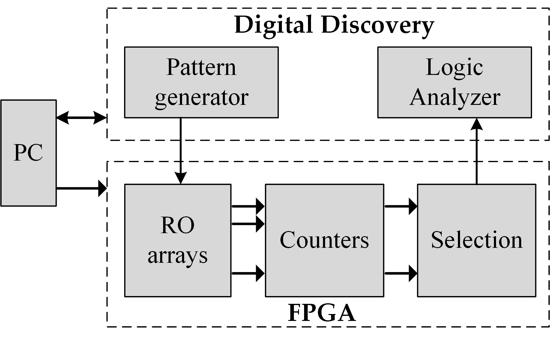
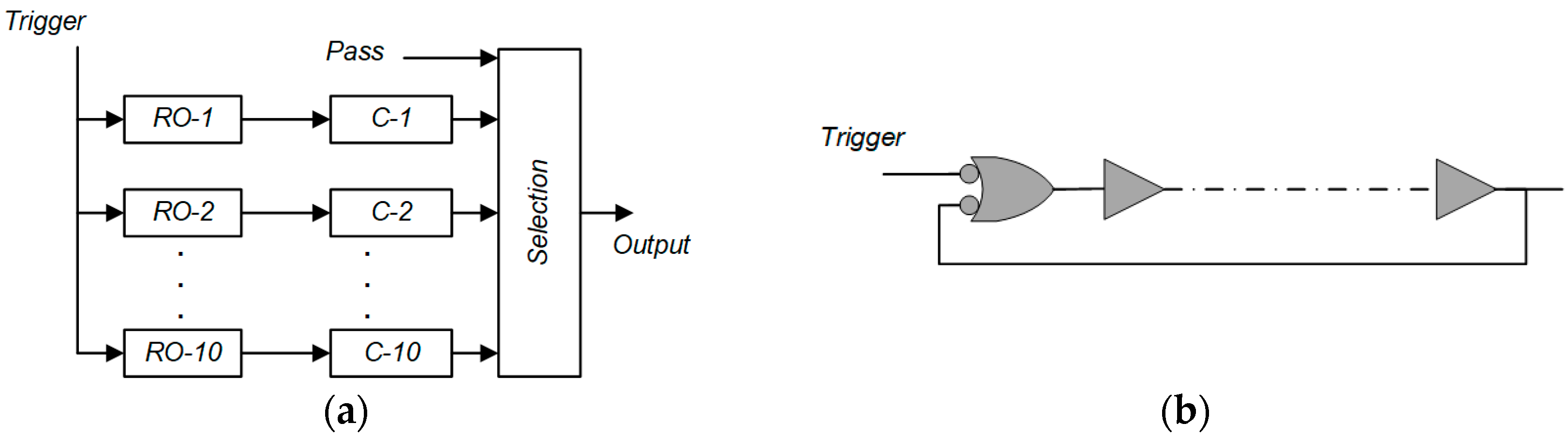
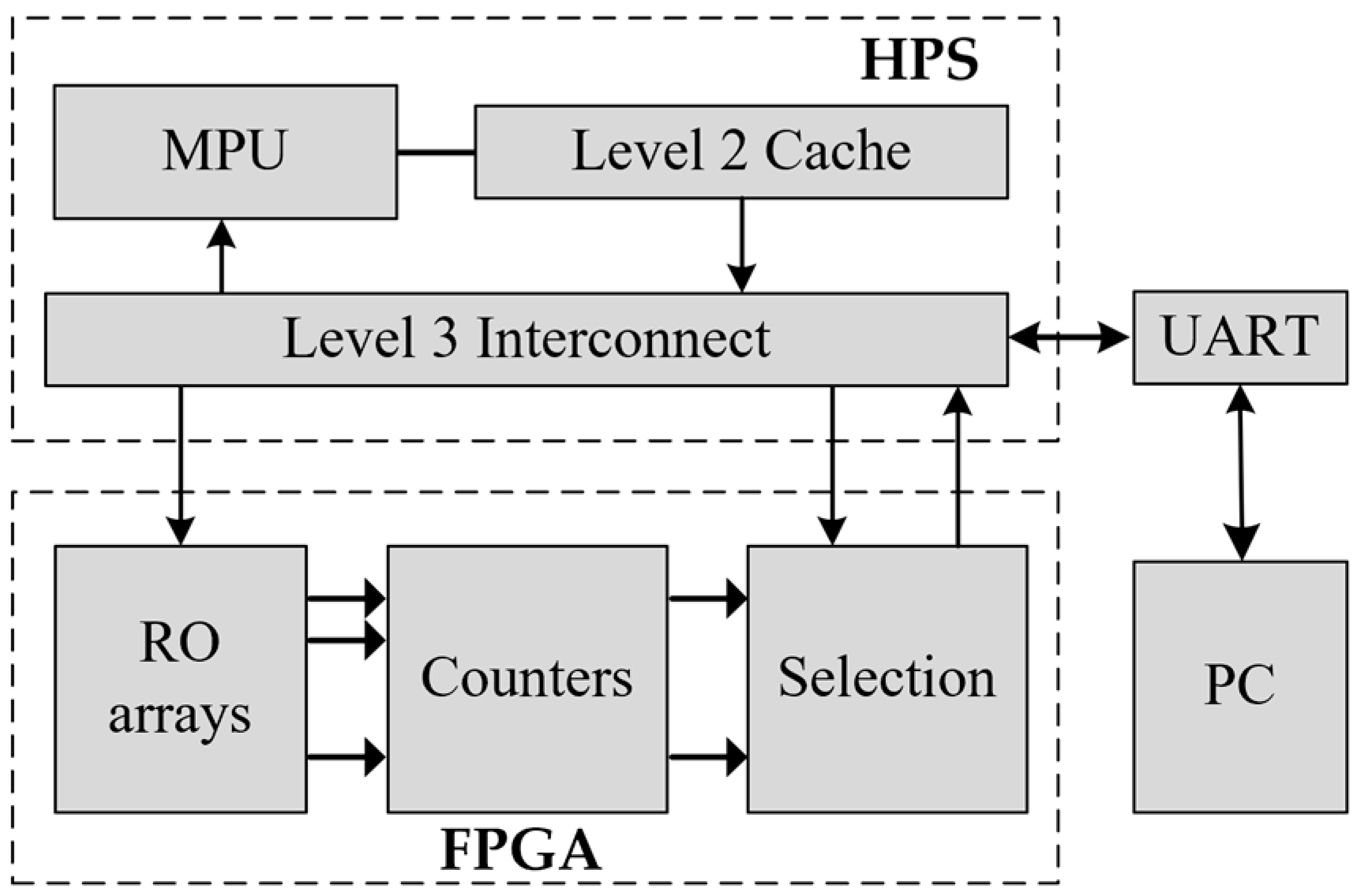
3. Ring Oscillator PUF Scheme

3.1. Frequency Measurement

Most of the proposed RO-PUFs extracted bit responses by comparing RO pairs. Those methods are not flexible due to the limited responses [9,15]. Therefore, this work extracts RO frequency directly by counting pulses, as shown in Figure 1, during the characterization process [20]. The extraction procedure aims to evaluate the exact number of pulses. The measurement is realized using a PC, FPGA boards, and Digital Discovery. ROs are activated simultaneously during a defined period controlled by the pattern generator.
The pulses of ROs that are counted simultaneously are then passed into the logic analyzer. The process may be carried out a bit slower to ensure that the logic analyzer samples values precisely, since they remain inside counters after ROs are disabled. The values are then stored in a CSV file format and converted to frequencies. The measurement was carried out repeatedly at specific low and high temperatures.
Each RO is connected directly to an individual counter, as shown in Figure 2a. Signal Trigger is used to activate the ROs during a specific period. The number of pulses counted by the counters is passed out of the chip after the ROs are disabled. Figure 2b shows the implemented ring oscillator on the Intel Cyclone V chip. Theoretically, the RO would be constructed from an odd number of gates (a NAND and a series of NOT gates). However, a straightforward implementation is not allowed on Cyclone V [3,21]. Therefore, the circuit is replaced by a negative NOR and a series of buffers with equal functionality. Moreover, the circuit in Figure 2b is more flexible because the RO constructed using an even number of gates can be established.

3.2. Identity Characterization

Resource consumption of the RO-PUF is becoming a serious issue since there is little space for establishing a primary system. Researchers proposed many ideas in order to reduce the area while keeping a large number of responses. In this case, an additional intermediary process is required to map the limited ROs that can produce enough response bits [10,20,22]. However, the scheme degrades uniqueness because it increases the possibility of frequency order among chips becoming similar. A solution using the Q factor to distinguish chips has been implemented, improving the uniqueness [17]. Hence, the identity of every chip is more apparent. Delavar et al. have proposed a slightly different idea to enhance the response bit so that it can also approach the ideal uniqueness [18].
However, those enhancement procedures further degrade the stability. Moreover, the FPGA chip of the 90 nm lithography process has become irrelevant. Recently, a new FPGA chip has been fabricated using a shorter transistor channel that narrows the pulse of the RO. Counting the exact number of pulses at such a high frequency is more challenging. Therefore, this study acquired data from the shorter transistor length chip, such as Cyclone V of 28 nm. Then, instead of using a three-stage RO, and due to higher frequencies, we prefer the higher-stage RO in order to achieve stable measurement and tackle the difficulty in capturing frequencies.
Establishing a limited RO-PUF may increase the probability of results from equal frequency orders. The resulting frequencies may differ among chips, but the order (i.e., sorted from low to high and vice versa) may be equal. Therefore, the unique frequency of individual chips using the Q factor should be considered in designing PUFs [17,18]. The Q factor, mapped from frequencies, aims to distinguish between chips. Therefore, Q may be calculated from the different frequencies of two, three, four, etc., ROs of the same chip, as shown in Equation (1).
Q p f 1 ,   f 2 , ,   f n 1 = i = 1 n 1     j = n + 1 n w . | f i f j | e
where 1 < p < n; this study set the weight factor w = 1 for simplification during the analysis and e = 0.5. In this case, all possible Q values can be estimated using Equation (2).
Q t o t a l = Q 2 + Q 3 + + Q n = n 2 + n 3 + n 4 + + n n = 2 n n 1
We evaluated Q’s randomness by comparing chips from all experiments. The Kolmogorov–Smirnov test is used to assess whether or not it accepts the hypothesis that two samples are different (h = 1) or similar (h = 0). All of them passed the Kolmogorov–Smirnov test [23]. Therefore, using Q to extract the identity of chips can be considered to increase the number of responses.

3.3. Response Generation

Conventionally, RO-PUF responses are generated by comparing neighbors’ frequencies. Many scenarios have been proposed to approach ideal uniqueness and reliability. Some achieved good metrics [9,15,24,25]. However, those methods lead to resource consumption. A further process (outside the FPGA chip) is required, which may cause inefficiency in establishing such an identity or security procedure due to the huge resources. Table 1 compares the number of CRPs in several RO-PUFs and the location of the enhancement circuit. Among the proposed methods, Maiti and Delavar enhanced response methods using limited resources [17,18]. The identity characterization, which is mapped from frequency sets to distinguish the chip, requires further mapping to extract the responses.
This work exploits the hard processor’s response generation process [17]. The Qs are converted to produce a set of responses using a quantization level. The range of Q values is divided into several equal intervals (quantization level l) with a width of q during response generation. The width of the interval of any chip is defined based on a range of Qs of a particular chip, i.e., q = (max(Q) − min(Q))/l. Any Qni of chip i falling within an interval is assigned the corresponding binary digit to create response Rni. Therefore, a binary output Rti is derived based on Equation (3) during the response generation.
R t i = 1 ,   if   Q t i   falls   inside   odd   interval 0 ,   if   Q t i   falls   inside   even   interval
Hence, the quantization level plays a vital role in generating responses. Therefore, the quantization level should be selected carefully to avoid further bit flips upon environmental change. This study estimates the number of CRPs (nC2 + nC3) based on factor Q and the response’s bit flip analysis. Later (Section 5.4), this study shows the response shifting due to quantization levels that affect uniqueness and reliability. Then, we proposed selected Qs to improve reliability.

3.4. Resource Utilization

The availability of a PUF circuit aims to provide hardware-based identification and security. During operation, the circuit is activated once to allow the user access to the chip contents. After that, the PUF is unused or idle. Therefore, the resources utilized to establish PUFs should be as low as possible. This issue encouraged the researchers to develop a PUF that utilized a small amount of resources. However, since most previous methods required additional resources outside the FPGA chip, they are challenging to implement due to the absence of such advanced mathematical calculations [14,17,18].
A new FPGA chip may contain a built-in processor (such as Intel Cyclone V and Zynq 7000, including Cortex A-9 ARM). In this case, the all-in-one chip PUF circuit may be established. Therefore, this study realizes the CRP enhancement all-in-one chip PUF process, as shown in Figure 3. The challenge is provided via a Universal Asynchronous Receiver/Transmitter (UART) from the PC (for example) to a hard processor (HPS). Communication between HPS and FPGA is performed using AXI connections (in the case of Cyclone V). The connection allows HPS to control the RO arrays. The HPS controlled the duration of the RO activation. Then, the counters hold the values (number of pulses) after the RO is disabled. The HPS orders the selection circuit to pass the counter values one by one. The remaining processes (CRP enhancement procedures) are performed using an HPS. The response will be transferred to the PC.
The design and experiment of this study can be migrated to other FPGA platforms as long as the chip contains a built-in processor. However, adjustments are required since the size of the CLB in Xilinx FPGAs (for example, Zynq 7000) is different. In Quartus, a series of buffers, as shown in Figure 2b, is implemented using primitive LCELL, while in Xilinx, they can be realized using LUT1. Various RO stages are arranged, such as 5, 11, and 20, which can also be realized in the Xilinx chip. However, the 20-stage RO is not possible since the CLB of Zynq 7000 consists of only 16 LUTs. Consequently, the size of the counter also needs to be reduced to achieve equal routing. This adjustment affects the duration of ROs that are activated to be reinvestigated [16].

4. Evaluation and Stability Improvement Scenarios

4.1. PUF Metrics

The metrics in terms of uniqueness, reliability, uniformity, and bit aliasing of the RO-PUF are investigated in this work. The hamming distance (HD), which is determined by Equation (4) [26], is used to determine uniqueness based on the difference in response bits between chips. Here, c is the chip number, rb is the number of response bits, Ru and Rv are the response bits of the u and v chips under comparison, and HD(Ru, Rv) is the Hamming distance between the response bits. As a result, the uniqueness might be assessed in the following way:
U n = 2 c c 1 u = 1 c 1   v = u + 1 c ( H D R u , R v / r b ) × 100 %
The ideal uniqueness is 50% of the circuit implemented on many chips. Otherwise, the value would not equal 50%, which indicates that the number of “1” and “0” in a series of responses is not equal. The shift in ideal uniqueness is as formulated in Equation (5) [27].
U s h i f t = ( 1 c 2 c 1 ) × 100 %  
Equations (6) and (7) were used in this work to calculate reliability based on the consistency of pulses at various temperatures [14]. The response bit from chip i at low temperatures is denoted by Rs, and the t-th sample of the R’s response bit from chip i at higher temperatures is denoted by Rs,t. The number of tests on the same chip is represented by k.
H D   I n t r a = 1 k t = 1 k H D ( R s , R s , t ) r b  
R e l = ( 1 H D I n t r a ) × 100 %
Responses with “1” and “0” in a string of bits are assessed using additional RO-PUF metrics. Bit aliasing estimates the unpredictability of a specific bit’s answer in a collection of chips, whereas uniformity establishes the randomness of a particular chip’s responses. The number of “1” and “0” in a sequence of response bits is identical when the ideal uniformity and bit aliasing are 50%. According to Equation (8), uniformity is determined by comparing the Hamming weight (HW) of “1” on the same chip, where Rs,l is the l-bit from a specific chip’s response bit sequence. Equation (9) measures bit aliasing based on the Hamming Weight of “1” among a set of chips, where Rs,j is the j-bit from the sequence of response bits of a chip group.
U n i f o r m i t y = 1 r b l = 1 r b R s , l × 100 % ,
B i t a l i a s i n g = 1 c l = 1 c R s , j × 100 % ,

4.2. Proposed Frequency Mapping

The response of a PUF may flip due to environmental change, i.e., temperature and supply voltage. In the case of RO-PUFs, the close frequency pairs tend to contribute to this phenomenon when they are mapped to produce a response via an intermediary process. Therefore, this study introduces a new way of mapping frequencies based on the recorded pulses. The idea is to shift the frequencies slightly to acquire equal differences among them. Let us illustrate our concept by considering the five frequencies of f1 = 200 MHz, f2 = 210 MHz, f3 = 201 MHz, f4 = 220 MHz, and f5 = 218 MHz.
First, sort them (frequencies) from low to high as follows:
f1 = 200, f3 = 201, f2 = 210, f5 = 218, f4 = 220
Hence, the difference in frequencies is as follows:
df1,3 = 1 MHz, df3,2 = 9 MHz, df2,5 = 8 MHz, df54 = 2 MHz
Second, estimate the equal difference among the closest frequencies.
dfequal = (fmax − fmin)/(n − 1) = (220 − 200)/4 = 5 MHz
Third, map the frequencies into new values:
f1 = 200, f3 = 205, f2 = 210, f5 = 215, f4 = 220
After that, with these equal differences among frequencies, calculate the Q values [17]. As described in Algorithm 1, this procedure is used to perform our proposed frequency mapping.
Algorithm 1 Proposed step for frequency mapping
f_temp = [Initial f]; --reads frequencies and their position
f_sort = sortrows(f_temp,2); --sorts frequencies
f_dif = range(f)/(n − 1); --calculates average difference
f_sort(1,2) = min(f); --reads out minimum frequency
for p = 2: n
      f_sort(p,2) = f_sort(p-1,2) + f_dif; --maps into new values
end
f_re_sort = sortrows(f_sort,1); --reposition frequencies to initial

4.3. Proposed Response Generation

During the response generation process, this study analyzed the reduction in reliability by evaluating every single bit of the response. This study found a direct correlation between the Q factor and response bits. Any shift in Q values might be mapped into different quantization levels (even or odd levels), which would generate different responses between low and high temperatures (25 °C and 50 °C, as shown in Table 2). Therefore, it will also increase the bit flip of the response.
Table 2. Experimental specifications and conditions of RO-PUF in 28 nm Intel Cyclone V.
ItemsSpecification/Condition
ChipCyclone V
Hard ProcessorARM Cortex A-9
Lithography28 nm
No. of chips11
Temperatures25 °C, 50 °C
Recorded frequency11,000
RO placementFixed location
Routing hotspotsUniform [16]
No. of ROsTen
Measurement toolsPattern Generator, Logic Analyzer
Therefore, this work excludes several Q values to reduce bit flips based on the evaluation Q that will be discussed in Section 5.2. In the end, it is expected to increase reliability. Consequently, the reduction will reduce the number of response bits. This work evaluates the reduction in the number of response bits and how much the reliability improves. A detailed discussion is covered in the next section.

5. Results

In most RO-PUF designs, all circuits are placed inside the chip. This placement reduces the space for primary circuits. A new FPGA chip equipped with a microprocessor may be used to process the PUF while using a small amount of FPGA resources. This study left more space for primary circuits by shifting the process of generating responses using the built-in microprocessor. The direct connection of the Advanced eXtensible Interface (AXI) transfers frequencies (counter values) to the microprocessor. The experimental conditions of this work are summarized in Table 2.

5.1. Metric Evaluation

The procedure to evaluate the PUF’s metric (uniqueness and reliability) is as follows:
  • Activate ROs during a specific time.
  • Read counter values out of the chip.
  • Convert the values into frequencies.
  • Calculate Q values (Q2, Q3, … Qn−1).
  • Set quantization to level (denoted as ql).
  • Generate response bits.
  • Calculate uniqueness and reliability.
A set of data using the procedure is listed in Table A1 in the Appendix A. The results show step-by-step processes until the responses are generated. This study evaluates the CRP-enhanced method of uniqueness and reliability using original data; Figure 4 shows uniqueness and reliability vs. quantization levels. The calculation is performed under nine quantization levels (ql = 4, 6, 8, 10, 12, 16, 20, 28, and 32). It can be seen that as the quantization level increases, the uniqueness rises to approach the ideal value. However, on the other hand, the reliability decreases significantly. Therefore, this study evaluates further Q values that affected the reduction in the reliability of all quantization levels.

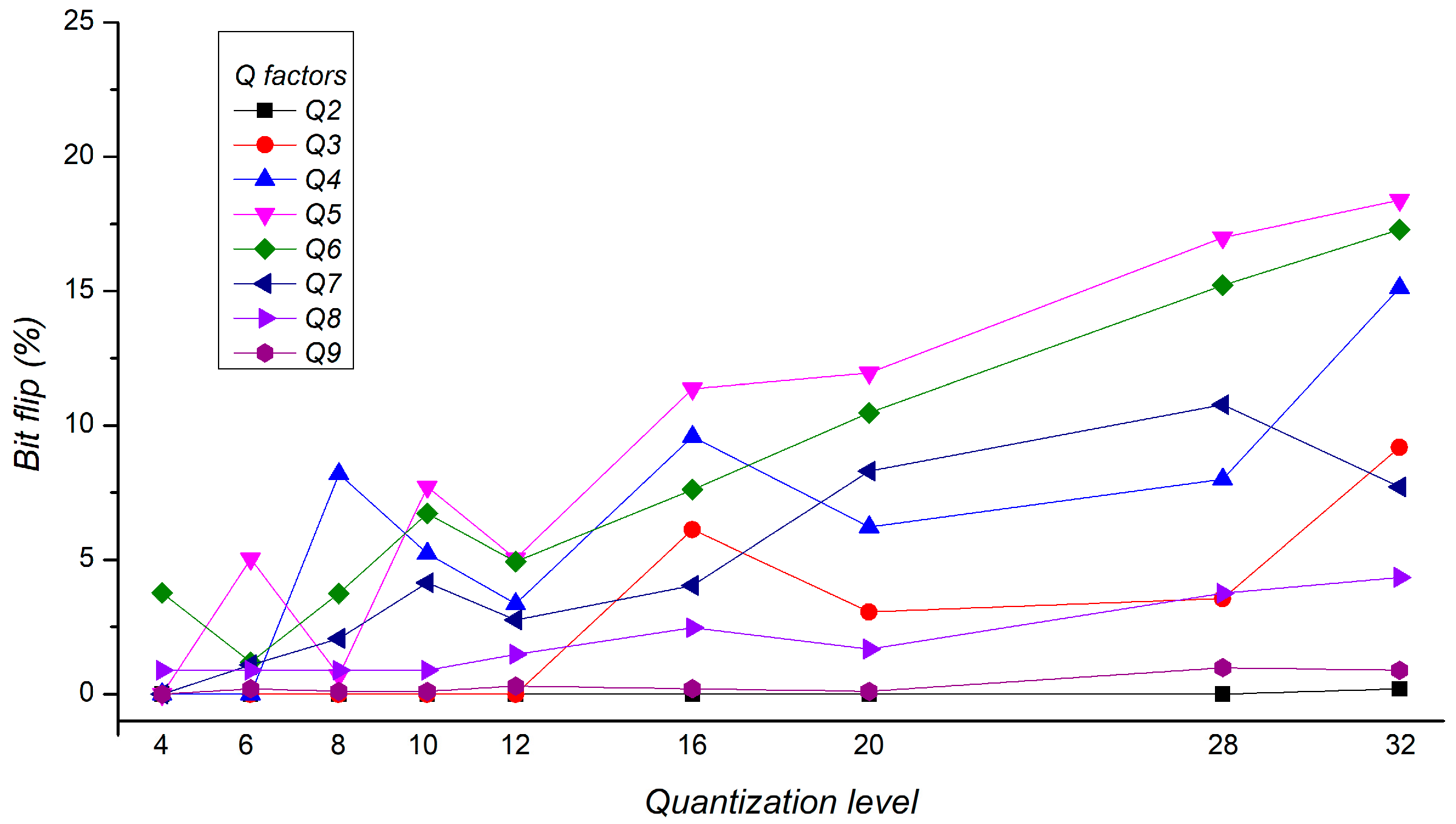
5.2. Bit Flip Contribution of Q

The Q values depend on frequency differences among ROs (Equation (1)); choosing a suitable RO stage has become challenging since the frequency depends on the delay of the series inverters. This study evaluates frequency differences of 5-, 11-, and 20-stage ROs. For example, the five-stage RO, with an average frequency of 436 MHz, has an average difference among frequencies of 1.18 MHz. For 11 stages (average frequency 219 MHz), the frequency difference among ROs is 0.44 MHz, while the 20-stage ROs, with a 108 MHz average frequency, have an average frequency of 0.22 MHz. Q values are classified as follows, with ten ROs (ten frequencies) and based on Equation (1).
  • Q2 and Q8: each 45 values.
  • Q3 and Q7: each 120 values.
  • Q4 and Q6: each 210 values.
  • Q5: 252 values.
  • Q9: 10 values.
Based on the evaluation in Section 5.1 regarding metric performance, as shown in Figure 4, this study identifies every single response bit to seek those that contribute to bit flips. Since the response bit is associated directly with Q, this work identifies any Q values that affected the reduction in reliability. This work compares responses at low and high temperatures; hence, any bit flip exists marked and associated with specific Q values. Figure 5 shows, in percentages, the extent to which bit flips are affected by Q versus the quantization level.

5.3. Improvement of Q

When many ROs are realized, the total Q also increases. For instance, a realization of six ROs generates 57 total Qs, and a realization of ten ROs would result in 1013 Q values, based on Equation (2). Moreover, the calculation complexity increases significantly as the number of Qs increases. Table 3 shows the calculation complexity of Qs for a single individual value. Therefore, a trade-off between the number of Qs and calculation complexity should be considered.
This work further evaluates the Q shift upon temperature change regarding reliability reduction. For instance, Figure 6 compares Q2 at low and high temperatures (fifth column in Table A1). The Q is calculated from data on an experiment of chip 2. As can be seen, significant changes exist in Q2(4), Q2(9), Q2(16), and Q2(35). When these Qs are used to generate a response, it might be flipped because they will fall inside different levels (i.e., Q2(4) at low temperatures falls inside an odd level; in contrast, Q2(4) at higher temperatures falls inside an even level). Therefore, the significant differences in Q between high and low temperatures should be reduced.
This work proposes a new frequency mapping that aims to reduce those significant differences. When the proposed frequency mapping is applied (Section 4.2), the significant difference in Qs between low and high temperatures becomes tiny. Figure 7 compares Q2 at low and high temperatures in chip 2 after applying the new frequency mapping. There is no significant change in Qs, as can be seen from the figure. This tiny change is because the difference in frequencies among ROs has become uniform. Therefore, it is expected that the bit flip might be reduced. Hence, the reliability would be higher.
Using the proposed frequency mapping, the significant difference in Qs between low and high temperatures becomes tiny. This change is due to uniform frequency differences among ROs.

5.4. Improvement in Response

During response generation, the quantization level ql is essential in mapping a set of Q values to responses. When ql is chosen to be small (i.e., ql = 4), the reliability will increase, but the uniqueness will decrease to an unacceptable score, as seen in Figure 4. This reduction in reliability due to bit flips might also be associated with a particular Q, as the quantitation level is higher. This trend can be seen in Figure 8, where the bit flip tends to increase at higher quantization levels.
Based on the bit flip trend in Figure 8 and considering the quantization level shown in Figure 4, this study recommends the following scenarios:
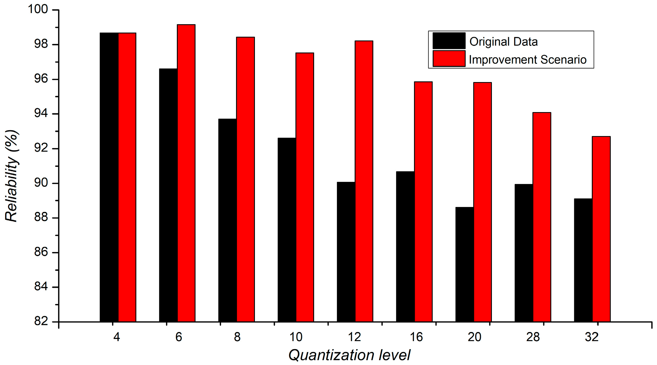
  • Apply Q improvement using the proposed frequency mapping. As Qs are extracted to distinguish among chips, the shift in frequency difference between low and high temperatures causes lower reliability. The frequency mapping is proposed to uniformize frequency differences and improve Qs, as shown in Figure 7.
  • Consider Qs that contribute fewer bit flips. Response bits are generated using several Qs, for instance, Q2, Q3, Q8, and Q9 (others are neglected). Exclusion is based on a detailed analysis, as can be seen in Figure 5, where Q4, Q5, and Q6 contribute a significant bit flip. The response is expected to be more immune to temperature change, even though this scenario produces fewer response bits.
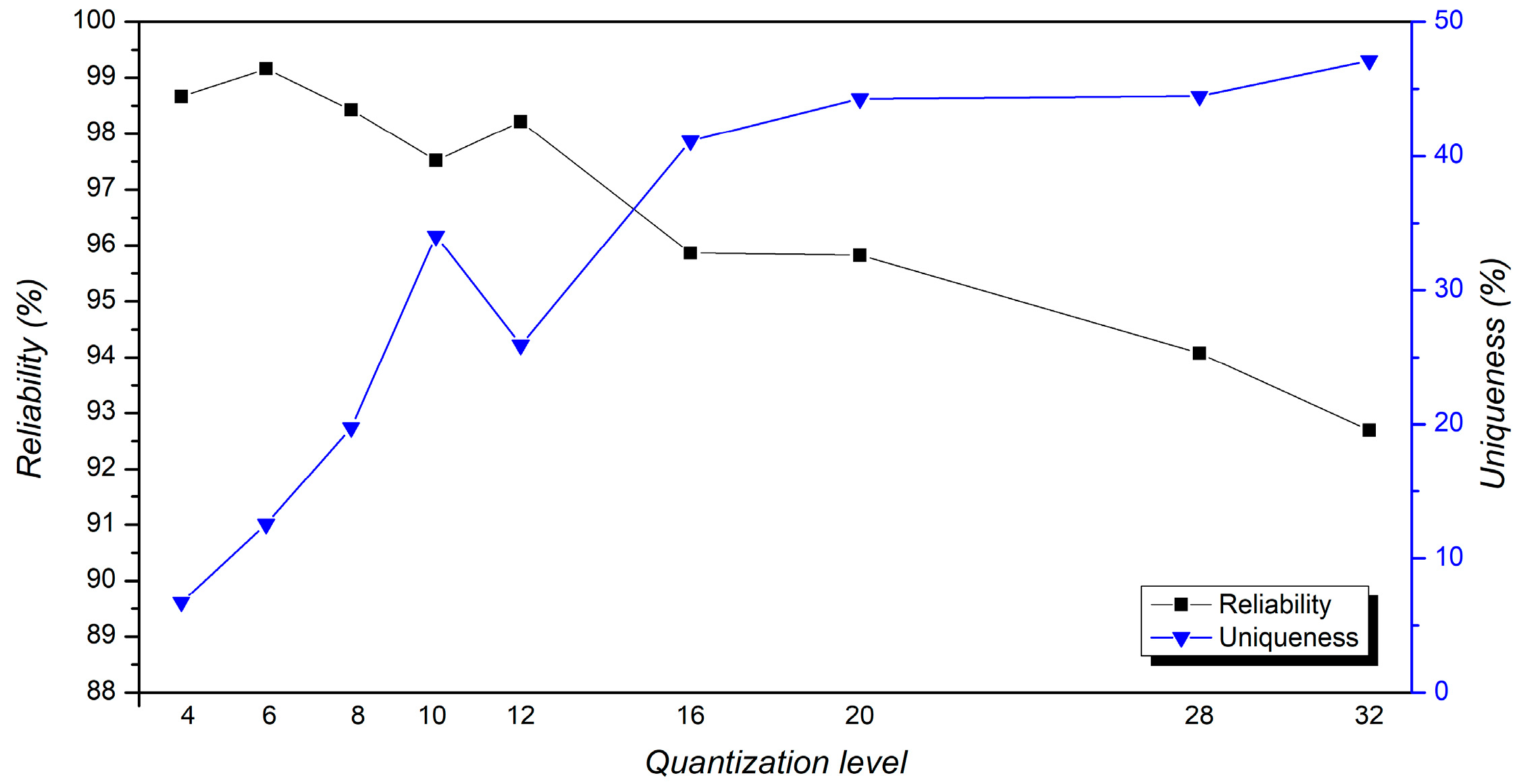
  • Choose a quantization level that balances reliability and uniqueness. This work suggests generating responses using a quantization level of ql = 16. At this point, the reliability is around 95.8%, which is acceptable, and the uniqueness is approximately 42%. The score is also acceptable since the ideal uniqueness value is estimated using 11 chips, implying that uniqueness is less than 50% [22]. The selected quantization level affects responses when higher Q values are involved because the levels derived from a range of Q values shift.
This work also analyzes further Qs regarding the required resources or calculation complexity upon implementation, as shown in Table 3. As Qs are based upon frequency differences of two, three, and more ROs (Equation (1)), this study considers using only Q2 and Q3. Those scenarios are not limited to this study and can also be applied to other designed RO-PUFs based on a particular technology. Figure 9 shows the metric (reliability) of the RO-PUF with CRP enhancements between the original data and the data after applying the improvement scenario. It can be seen that the reliability improves of all selected quantization levels. The tiny improvement in reliability is when the responses are generated using ql = 4. This small increase is because the reliability almost achieves an ideal value.

5.5. Uniformity and Bit Aliasing

In the conventional RO-PUF, the responses are generated naturally by comparing the frequency variation in RO arrays without post-processing. The response may contain an unequal number of “1” and “0”. Hence, the uniformity and bit aliasing are unpredictable. On the other hand, this work generates responses based on Qs that fall into odd or even quantization levels. Theoretically, the uniformity and bit aliasing may approach ideal values of 50% when the PUF is tested in many devices. We found that the values were subject to change based on the quantization level, ranging from about 51% to 61%, as the quantization level decreased. As per the discussion in Section 5.4, this study suggests quantifying Q using ql = 16; at this point, both uniformity and bit aliasing scores are 56.97%. This value is acceptable since the results were obtained from 11 devices.

5.6. Performance Comparison

This study examined how well the novel frequency mapping RO-PUF performed regarding bit aliasing, uniqueness, uniformity, and dependability compared to previous studies. Although some work has been conducted on Altera (Intel) FPGAs, most of the suggested RO-PUFs in the literature use Xilinx FPGAs. The measurements from this experiment and the published works are compared in Table 4. In some previously published research, the authors used various strategies to increase RO quality [3,15,17,24]. Most previously suggested works are unsuitable because they require significant space for the regulating circuit, CRP production, or RO creation. Due to CRP boosting approaches, we discovered that the concepts put out by Maiti et al. [17] and Delavar et al. [18] are applicable. However, both designs have lower reliability scores.
Based on the concept of PUFs proposed by Delavar et al. [18], Chauhan et al. [25] suggested an alternative frequency characterization to increase reliability. However, significant space was needed because no expanded CRP techniques were applied during response production. Deng et al. and Abulibdeh et al. suggested employing hybrid logic gates to alter the configurable ring oscillator (C-RO) [26,28]. However, the studies did not categorize or define the influence of aging that can modify the frequency when comparing RO-PUFs [29,30,31]. For example, the frequency may be deteriorated by high temperatures and the time required to extract data from chips. Therefore, the proposed structure is tested at no more than 50 °C.
Bernard et al. (2012) initially realized the ROs as PUFs on Altera in the literature, utilizing Cyclone II and Cyclone III on a comparable FPGA architecture [32]. Nevertheless, the study made no mention of metrics. Feiten et al. [3] used Cyclone IV to realize the RO-PUF. They provided a detailed description of Altera FPGA’s implementation; however, they were unable to increase its uniqueness.
Regarding huge resource consumption that limits the space for the primary circuits, some works in the literature have successfully carried out the chip CRP process [19]. However, additional large resources may be difficult to realize. This situation can compromise selected FPGA chips that contain built-in processors such as Zynq 7000 and Cyclone V series. As can be seen from Table 4, this work’s metric (uniqueness: 42%; reliability: 95.8%) is acceptable because it is extracted using 11 devices, where the ideal uniqueness is 45% (Equation (5)). In comparison, Martinez et al. [19], who utilized a built-in processor, tested the algorithm using only three devices, with an ideal uniqueness shift of 50%.
This work established ten ROs of 5, 11, and 20 stages onto Cyclone V. Consequently, ten 20-bit counters are used to record the pulses resulting from ROs by considering runtimes suggested in [16] to avoid pulses falling inside gray areas, which might lower reliability. Initially, the design required 355 ALMs and 290 FFs in the case of a 20-stage RO implementation, which is equal to 1% of the available resources in the chip (5CSEMA5F31C6). However, most of the area was used by control circuits. Upon realization of a fixed runtime, resource usage may be reduced. This work requires 100 ALMs for ring oscillators, 105 ALMs and 200 FFs for realizing counters, and 105 ALMs and 35 FFs for selection, in order for the circuit to pass the counter values. When each ALM contains two LUTs, the design approximately draws a maximum of 420 mW of static power.
Table 4. Comparison of resource utilization and RO-PUF metrics.
Uniqueness (%)Reliability (%)Uniformity (%)Bit Aliasing (%)
Suh et al. [9], 200746.1599.52--
Maiti et al. [10], 200935.91–45.90---
Xin et al. [33], 201132, 4199.29--
Maiti et al. [17], 201149.99–50.07±92 *, ±70 *50.02, 49.450.02, 49.4
Feiten et al. [3], 20136.68–37.0399.41–82.550.00, 62.07-
Sahoo et al. [4], 201347.5790.70 **4714.95
Kodytek et al. [24], 201648.42–48.7498.22, 97.55--
Delavar et al. [18], 201649.8196.07--
Chauhan et al. [25], 201949.997.85–99.80--
Deng et al. [26], 202049.9591.4–99.13 *49.61-
Zulfikar et al. [14], 202150.18 #99.51 #47.5562.98
Martinez et al. [19], 202247.52–48.9496.84−98.53--
This work42% #95.8% #56.97 #56.97 #
* Approximation, ** reliability measured in room temperature, and # best result (quantization level ql = 16).

6. Conclusions

Using a built-in hard processor can reduce the area of an RO-PUF since it is used once the chip is accessed. Using the intermediary process to generate more responses using frequency mapping is a promising solution. The proposed new frequency mapping shifts the frequencies slightly to acquire equal differences among them. Then, by considering Q2 and Q3, the improvement scenario proved able to increase the metric compared to previous enhanced CRP models, especially reliability, which improves significantly to 95.8% using a quantization level of 16, as shown in Table 4. The procedure explained in this work might be implemented in other chips of Intel, Xilinx, and other platforms as long as the built-in hard processor exists. This research may be improved further to suit more application requirements for integrated circuit identity. For instance, to prevent a change in routing equality between ROs and counters when the primary circuit is established, the proposed design should be isolated in a specific area, which would require hardware macro calibration.

Author Contributions

Conceptualization, Z.Z. and H.W.; methodology, Z.Z. and K.M.; software, Z.Z. and K.M.; validation, Z.Z., A.R. and K.M.; formal analysis, H.W.; investigation, Z.Z.; resources, Z.Z.; data curation, K.M.; writing—original draft preparation, Z.Z. and A.R.; writing—review and editing, Z.Z. and H.W.; visualization, A.R.; supervision, Z.Z. and K.M.; project administration, H.W.; funding acquisition, Z.Z. All authors have read and agreed to the published version of the manuscript.

Funding

This research was funded by the Ministry of Education, Culture, Research, and Technology under PFR-DRTPM (Grant No. 094/E5/PG.02.00.PL/2024).

Data Availability Statement

The original contributions presented in this study are partially included in the Appendix A. Further inquiries can be directed to the corresponding author(s).

Conflicts of Interest

The authors declare no conflicts of interest.

Abbreviations

The following abbreviations are used in this manuscript:
RO-PUFRing Oscillator Physical Unclonable Function
CRPChallenge and Response
FPGAField-Programmable Gate Array
PCPersonal Computer
UARTUniversal Asynchronous Receiver/Transmitter
HPSHard Processor
HDHamming Distance
HWHamming Weight
AXIAdvanced eXtensible Interface

Appendix A

Table A1 shows a complete set of examples of data used and or calculated in this work, starting from captured counter values (measurement) until the final step of response generation. The data was taken from the first experiment in chip 2 at low temperatures using a five-stage RO. First of all, ten counter values were carried out on the chip (second column in Table A1). The frequency is calculated with respect to the duration of an RO activation of 1 ms (third column in Table A1). Then, frequencies are mapped into new values (fourth column in Table A1) using the proposed Algorithm 1 (Section 4.2). Based on these frequencies, Qs are calculated. To simplify, Table A1 lists only Q2, which contains 45 values (fifth column in Table A1). Then, the responses associated with Q2 are generated using a quantization level of ql = 6 (column 6 in Table A1).
Table A1. Example: a set of data measurements until responses are generated.
No.Measurement (Pulse)Frequency (MHz)Proposed Freq. Mapping
Frequency (MHz)
Q2Response
1434,405434.405436.80866671.0869941
2433,389433.389435.62711112.4305921
3440,266440.266442.71644442.1739881
4437,535437.535441.53488891.0869941
5434,414434.414437.99022221.8827290
6433,264433.264433.2642.662581
7443,898443.898443.8981.8827291
8436,520436.52440.35333331.5372411
9433,556433.556434.44555561.5372411
10434,452434.452439.17177782.662580
11---2.4305920
12---1.5372411
13---1.5372411
14---2.8759150
15---2.1739880
16---1.0869941
17---1.8827291
18---1.0869941
19---2.1739880
20---3.0744830
21---1.0869941
22---1.5372411
23---2.8759150
24---1.8827291
25---1.8827291
26---2.8759150
27---1.5372411
28---1.0869941
29---2.662580
30---1.5372411
31---2.1739881
32---2.4305920
33---1.5372411
34---1.8827291
35---1.0869941
36---3.2609810
37---2.662580
38---1.0869941
39---2.4305921
40---1.8827291
41---3.0744830
42---2.1739880
43---2.4305921
44---1.0869941
45---2.1739881

References

  1. Halak, B. Physically Unclonable Functions: From Basic Design Principles to Advanced Hardware Security Applications; Springer: Berlin/Heidelberg, Germany, 2018. [Google Scholar]
  2. Maes, R. Physically Unclonable Functions: Constructions, Properties and Applications; Springer Science & Business Media: Berlin/Heidelberg, Germany, 2013. [Google Scholar]
  3. Feiten, L.; Spilla, A.; Sauer, M.; Schubert, T.; Becker, B. Implementation and analysis of ring oscillator PUFs on 60 nm Altera Cyclone FPGAs. Inf. Secur. J. Glob. Perspect. 2013, 22, 265–273. [Google Scholar] [CrossRef]
  4. Sahoo, D.P.; Mukhopadhyay, D.; Chakraborty, R.S. Design of low area-overhead ring oscillator PUF with large challenge space. In Proceedings of the 2013 International Conference on Reconfigurable Computing and FPGAs (ReConFig), Cancun, Mexico, 9–11 December 2013; pp. 1–6. [Google Scholar]
  5. Karmakar, M.; Naz, S.F.; Shah, A.P. Fault-tolerant reversible logic gate-based RO-PUF design. Mem.-Mater. Devices Circuits Syst. 2023, 4, 100055. [Google Scholar] [CrossRef]
  6. Zhu, Y.; Fang, Y.; Hu, X.; Yang, R. Design and FPGA Implementation of a Password Management System Utilizing RO PUF. In Proceedings of the 2024 5th International Seminar on Artificial Intelligence, Networking and Information Technology (AINIT), Nanjang, China, 29–31 March 2024; pp. 303–307. [Google Scholar]
  7. Khan, S.; Shah, A.P.; Gupta, N.; Chouhan, S.S.; Pandey, J.G.; Vishvakarma, S.K. An ultra-low power, reconfigurable, aging resilient RO PUF for IoT applications. Microelectron. J. 2019, 92, 104605. [Google Scholar] [CrossRef]
  8. Abulibdeh, E.; Saleh, H.; Mohammad, B.; Al-Qutayri, M.; Santikellur, P. Boosted PUF: Boosting Efficiency and Resilience in Configurable RO PUF for IoT Devices. TechRxiv 2024. [Google Scholar]
  9. Suh, G.E.; Devadas, S. Physical unclonable functions for device authentication and secret key generation. In Proceedings of the DAC07: The 44th Design Automation Conference, San Diego, CA, USA, 4–8 June 2007; pp. 9–14. [Google Scholar]
  10. Maiti, A.; Schaumont, P. Improving the quality of a physical unclonable function using configurable ring oscillators. In Proceedings of the 2009 International Conference on Field Programmable Logic and Applications, Prague, Czech Republic, 31 August–2 September 2009; pp. 703–707. [Google Scholar]
  11. Yin, C.-E.; Qu, G. Obtaining statistically random information from silicon physical unclonable functions. IEEE Trans. Emerg. Top. Comput. 2014, 2, 96–106. [Google Scholar] [CrossRef]
  12. Giechaskiel, I.; Rasmussen, K.B.; Eguro, K. Leaky Wires: Information Leakage and Covert Communication Between FPGA Long Wires. In Proceedings of the 2018 on Asia Conference on Computer and Communications Security, Incheon, Republic of Korea, 4 June 2018; pp. 15–27. [Google Scholar]
  13. Ikeda, M.; Kang, H.; Iwamura, K. Direct challenge ring oscillator PUF (DC-ROPUF) with novel response selection. In Proceedings of the 2017 IEEE 6th Global Conference on Consumer Electronics (GCCE), Las Vegas, NV, USA, 24–27 October 2017; pp. 1–2. [Google Scholar]
  14. Zulfikar, Z.; Soin, N.; Wan Muhamad Hatta, S.F.; Abu Talip, M.S.; Jaafar, A. Routing density analysis of area-efficient ring oscillator physically unclonable functions. Appl. Sci. 2021, 11, 9730. [Google Scholar] [CrossRef]
  15. Merli, D.; Stumpf, F.; Eckert, C. Improving the quality of ring oscillator PUFs on FPGAs. In Proceedings of the 5th Workshop on Embedded Systems Security, Scottdale, AZ, USA, 24 October 2010; pp. 1–9. [Google Scholar]
  16. Zulfikar, Z.; Soin, N.; Wan Muhamad Hatta, S.F.; Abu Talip, M.S. Runtime analysis of area-efficient uniform RO-PUF for uniqueness and reliability balancing. Electronics 2021, 10, 2504. [Google Scholar] [CrossRef]
  17. Maiti, A.; Kim, I.; Schaumont, P. A robust physical unclonable function with enhanced challenge-response set. IEEE Trans. Inf. Forensics Secur. 2011, 7, 333–345. [Google Scholar] [CrossRef]
  18. Delavar, M.; Mirzakuchaki, S.; Mohajeri, J. A ring oscillator-based PUF with enhanced challenge-response pairs. Can. J. Electr. Comput. Eng. 2016, 39, 174–180. [Google Scholar] [CrossRef]
  19. Martínez-Rodríguez, M.C.; Rojas-Muñoz, L.F.; Camacho-Ruiz, E.; Sánchez-Solano, S.; Brox, P. Efficient RO-PUF for generation of identifiers and keys in resource-constrained embedded systems. Cryptography 2022, 6, 51. [Google Scholar] [CrossRef]
  20. Zulfikar, Z.; Soin, N.; Hatta, S.W.M.; Talip, M.S.A.; bin Jaafar, A. Uniformizing Routing Hotspots of Ring Oscillators on the Cyclone V FPGA for PUF Applications. In Proceedings of the 2019 IEEE Regional Symposium on Micro and Nanoelectronics (RSM), Putrajaya, Malaysia, 21–23 August 2019; pp. 176–179. [Google Scholar]
  21. Feiten, L.; Sauer, M.; Becker, B. Implementation of Delay-Based PUFs on Altera FPGAs. In Hardware Security and Trust; Springer: Berlin/Heidelberg, Germany, 2017; pp. 211–235. [Google Scholar]
  22. Maiti, A.; Schaumont, P. Improved ring oscillator PUF: An FPGA-friendly secure primitive. J. Cryptol. 2011, 24, 375–397. [Google Scholar] [CrossRef]
  23. Lopes, R.H.; Reid, I.; Hobson, P.R. The Two-Dimensional Kolmogorov-Smirnov Test; Proceedings of Science: Treste, Italy, 2007. [Google Scholar]
  24. Kodýtek, F.; Lórencz, R.; Buček, J. Improved ring oscillator PUF on FPGA and its properties. Microprocess. Microsyst. 2016, 47, 55–63. [Google Scholar] [CrossRef]
  25. Chauhan, A.S.; Sahula, V.; Mandal, A.S. Novel randomized placement for FPGA based robust ROPUF with improved uniqueness. J. Electron. Test. 2019, 35, 581–601. [Google Scholar] [CrossRef]
  26. Deng, D.; Hou, S.; Wang, Z.; Guo, Y. Configurable ring oscillator PUF using hybrid logic gates. IEEE Access 2020, 8, 161427–161437. [Google Scholar] [CrossRef]
  27. Maiti, A.; Gunreddy, V.; Schaumont, P. A systematic method to evaluate and compare the performance of physical unclonable functions. In Embedded Systems Design with FPGAs; Springer: Berlin/Heidelberg, Germany, 2013; pp. 245–267. [Google Scholar]
  28. Abulibdeh, E.; Saleh, H.; Mohammad, B.; Al-Qutayri, M.; Hussain, A. Kernel-based response extraction approach for efficient configurable ring oscillator PUF. Sci. Rep. 2025, 15, 5938. [Google Scholar] [CrossRef] [PubMed]
  29. Hsieh, M.-H.; Huang, Y.-C.; Yew, T.-Y.; Wang, W.; Lee, Y.-H. The impact and implication of BTI/HCI decoupling on ring oscillator. In Proceedings of the 2015 IEEE International Reliability Physics Symposium, Monterey, CA, USA, 13–23 April 2015; pp. 6A. 4.1–6A. 4.5. [Google Scholar]
  30. Karimi, N.; Danger, J.-L.; Guilley, S. Impact of aging on the reliability of delay PUFs. J. Electron. Test. 2018, 34, 571–586. [Google Scholar] [CrossRef]
  31. Maiti, A.; Schaumont, P. The impact of aging on a physical unclonable function. IEEE Trans. Very Large Scale Integr. (VLSI) Syst. 2013, 22, 1854–1864. [Google Scholar] [CrossRef]
  32. Bernard, F.; Fischer, V.; Costea, C.; Fouquet, R. Implementation of ring-oscillators-based physical unclonable functions with independent bits in the response. Int. J. Reconfig. Comput. 2012, 2012, 13. [Google Scholar] [CrossRef]
  33. Xin, X.; Kaps, J.-P.; Gaj, K. A configurable ring-oscillator-based PUF for Xilinx FPGAs. In Proceedings of the 2011 14th Euromicro Conference on Digital System Design, Oulu, Finland, 31 August–2 September 2011; pp. 651–657. [Google Scholar]
Figure 1. Block diagram of frequency extraction of ROs.
Cryptography 09 00036 g001
Figure 2. Internal structure during characterization process: (a) direct connection between RO and counter; (b) ring oscillator implemented onto Intel Cyclone V.
Cryptography 09 00036 g002
Figure 3. Proposed CRP enhancement of all-in-one chip RO-PUF.
Cryptography 09 00036 g003
Figure 4. Uniqueness and reliability vs. quantization level using enhanced CRP.
Cryptography 09 00036 g004
Figure 5. Bit flip contribution of Q versus quantization level.
Cryptography 09 00036 g005
Figure 6. Comparison of Q2 of low and high temperatures in experiment 1 of chip 2.
Cryptography 09 00036 g006
Figure 7. Comparison of Q2 of low and high temperatures in experiment 1 of chip 2 using the proposed frequency mapping.
Cryptography 09 00036 g007
Figure 8. Bit flip trend of Q versus the quantization level of the RO-PUF.
Cryptography 09 00036 g008
Figure 9. Reliability comparison of original data and the improvement scenario.
Cryptography 09 00036 g009
Table 1. Comparison of the number of CRPs and the location of the enhancement circuit.
AuthorNo. of CRPsCRP Enhance/Location
Suh et al. [9]n/8no/inside chip
Maiti et al. [10]n − 1no/inside chip
Merli et al. [15]n/2no/inside chip
Maiti et al. [17]2nn − 1yes/outside chip
Yin et al. [11]log2 n!no/inside chip
Delavar et. al. [18]2n − 1yes/outside chip
Zulfikar et al. [14]n!/2(n − 2)!yes/inside or outside
This worknC2 + nC3yes/outside chip
Table 3. Calculation complexity of each Q value of Q2, Q3, Q4, and Q5.
Factor QMathematical Expressions
SubtractionPower/SquareSummation
Q2110
Q3332
Q4665
Q510109
Disclaimer/Publisher’s Note: The statements, opinions and data contained in all publications are solely those of the individual author(s) and contributor(s) and not of MDPI and/or the editor(s). MDPI and/or the editor(s) disclaim responsibility for any injury to people or property resulting from any ideas, methods, instructions or products referred to in the content.

