Article

Wordline Input Bias Scheme for Neural Network Implementation in 3D-NAND Flash

Division of Materials Science and Engineering and Department of Semiconductor Engineering, Hanyang University, Seoul 04763, Republic of Korea
*
Author to whom correspondence should be addressed.
Biomimetics 2025, 10(5), 318; https://doi.org/10.3390/biomimetics10050318
Submission received: 10 April 2025 / Revised: 8 May 2025 / Accepted: 14 May 2025 / Published: 15 May 2025
(This article belongs to the Special Issue Advances in Brain–Computer Interfaces 2025)

Abstract

:
In this study, we propose a neuromorphic computing system based on a 3D-NAND flash architecture that utilizes analog input voltages applied through wordlines (WLs). The approach leverages the velocity saturation effect in short-channel MOSFETs, which enables a linear increase in drain current with respect to gate voltage in the saturation region. A NAND flash array with a TANOS (TiN/Al2O3/Si3N4/SiO2/poly-Si) gate stack was fabricated, and its electrical and reliability characteristics were evaluated. Output characteristics of short-channel (L = 1 µm) and long-channel (L = 50 µm) devices were compared, confirming the linear behavior of short-channel devices due to velocity saturation. In the proposed system, analog WL voltages serve as inputs, and the summed bitline (BL) currents represent the outputs. Each synaptic weight is implemented using two paired devices, and each WL layer corresponds to a fully connected (FC) layer, enabling efficient vector-matrix multiplication (VMM). MNIST pattern recognition is conducted, demonstrated only a 0.32% accuracy drop for the short-channel device compared to the ideal linear case, and 0.95% degradation under 0.5 V threshold variation, while maintaining robustness. These results highlight the strong potential of 3D-NAND flash memory, which offers high integration density and technological maturity, for neuromorphic computing applications.

1. Introduction

Artificial intelligence (AI) has advanced rapidly in recent years, driven by improvements in machine learning algorithms, increased computational power, and the availability of large datasets. However, conventional computing systems based on the von Neumann architecture suffer from inherent limitations due to the physical separation of memory and processing units [1]. This limitation, known as the von Neumann bottleneck, poses major challenges for real-time processing of large-scale data, particularly under the increasing demands of AI and edge computing. As conventional von Neumann computing architectures face fundamental limitations in energy efficiency and latency, neuromorphic computing, inspired by biological nervous systems, is increasingly considered a promising alternative. To overcome these limitations, computing-in-memory (CIM) has emerged as a promising solution. Unlike traditional architectures, CIM integrates computation within memory arrays, significantly alleviating data transfer bottlenecks and improving energy efficiency. This paradigm is especially well-suited for accelerating deep neural network (DNN) workloads [2,3,4,5,6,7,8,9,10,11,12].
DNNs, which drive advancements in AI, require highly efficient computational architectures. CIM has been recognized as a promising approach for accelerating core operations, such as vector-matrix multiplication (VMM), which are central to DNN computations. Various non-volatile memory devices, including resistive random-access memory (ReRAM) [13,14,15,16,17,18,19,20,21,22,23,24,25,26], phase-change memory (PCM) [27,28,29,30,31,32,33,34,35,36], and ferroelectric devices [37,38,39,40,41,42,43,44,45,46], have been investigated for CIM applications due to their distinctive properties. Among them, flash memory has gained significant attention in the CIM application [47,48,49,50,51,52,53,54,55,56]. In particular, NAND flash stands out as a highly attractive candidate owing to its high memory density, technological maturity, and excellent scalability. Compared to other emerging memory devices, its advanced development and manufacturing readiness make it especially suitable for the increasing demands of AI and edge computing systems.
However, 3D-NAND flash presents unique challenges, particularly in supporting analog input methodologies. The nonlinear current–voltage (IV) characteristics of field-effect transistors (FETs), combined with the vertically stacked architecture, complicate the processing of analog data inputs. Although several studies have explored binary or ternary input schemes via wordlines (WLs) [57], these approaches often suffer from accuracy degradation due to data loss associated with non-analog encoding. In contrast, analog input can minimize data loss and ensure a linear relationship between input and output, which is critical for fully connected (FC) layers. Nonetheless, implementing analog input remains difficult because of the quadratic dependence of drain current on gate voltage in a transistor. To address this issue, alternative methods such as bitline (BL)-based input and pulse-width modulation (PWM) techniques have been proposed; however, the implementation of multi-level inputs and weights in these approaches relies on shift-and-adder circuits, along with a large number of cells and BLs, leading to reduced area efficiency and cell density [58,59,60]. Additionally, analog inputs implemented using PWM introduce inference latency, which depends on the input values, while also requiring additional peripheral circuitry for input encoding. Lastly, analog input through BLs operating in the device linear region inherently limits the usable voltage range, thereby constraining the flexibility of analog signal representation.
In this work, we present a method for applying analog input through WLs while maintaining the conventional input/output terminal configuration of the 3D-NAND flash architecture and preserving analog data processing. This approach utilizes the velocity saturation effect observed in short-channel devices, where under high drain voltage conditions, the electric field between the source and drain becomes sufficiently strong to saturate carrier velocity. Consequently, the drain current exhibits a near-linear dependence on gate voltage, unlike the quadratic behavior observed in long-channel devices. By exploiting this characteristic, we can achieve the representation of linear analog input through the WLs, with a relatively wider range compared to the BL-based scheme. Also, by utilizing two distinct memory states, program (PGM) and erase (ERS), within a wide memory window that provides a large difference in current, the proposed scheme exhibits strong tolerance to threshold voltage variations. A charge trap-flash (CTF)-based NAND array was fabricated using a TANOS (TiN/Al2O3/Si3N4/SiO2/poly-Si) flash stack, and its electrical and memory characteristics were experimentally evaluated. Transfer characteristics were compared across devices with different gate lengths, confirming the linear response of short-channel devices. The current-voltage characteristics were applied to a neural network, and the system performance was analyzed against an ideal software-based linear input function. In addition, the robustness of the system was evaluated under threshold voltage variation in the PGM state, demonstrating its suitability for analog neural computing.

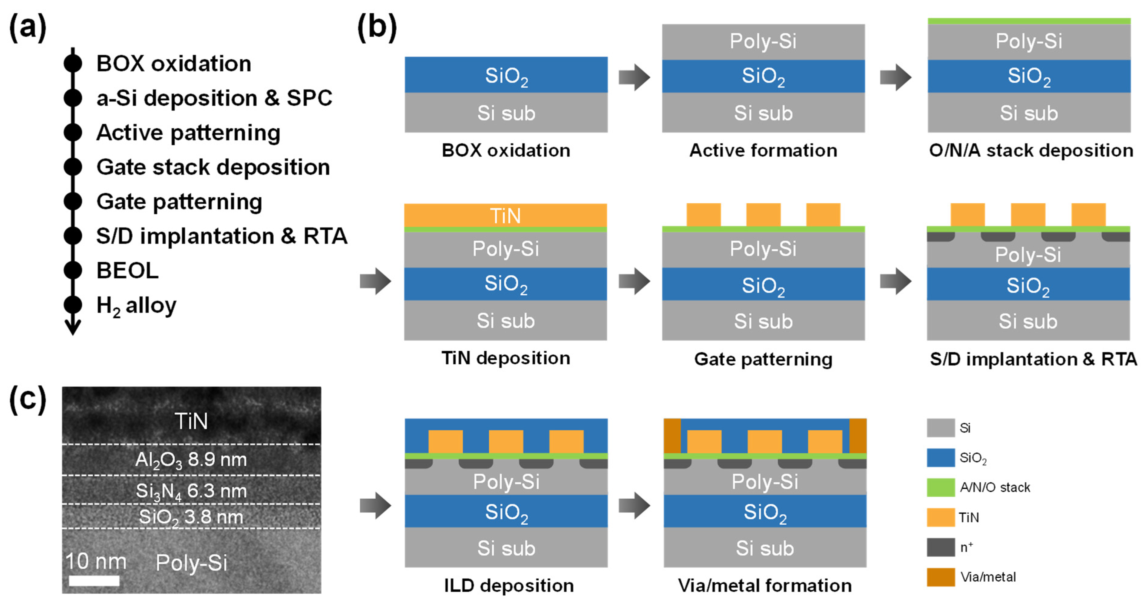
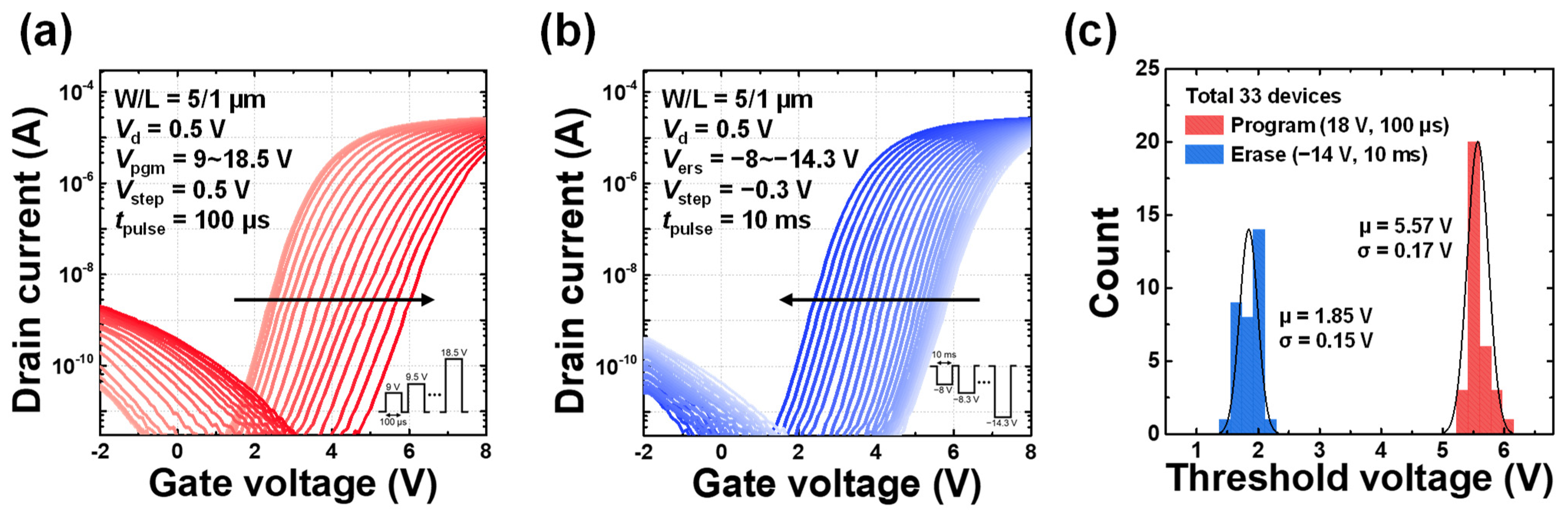
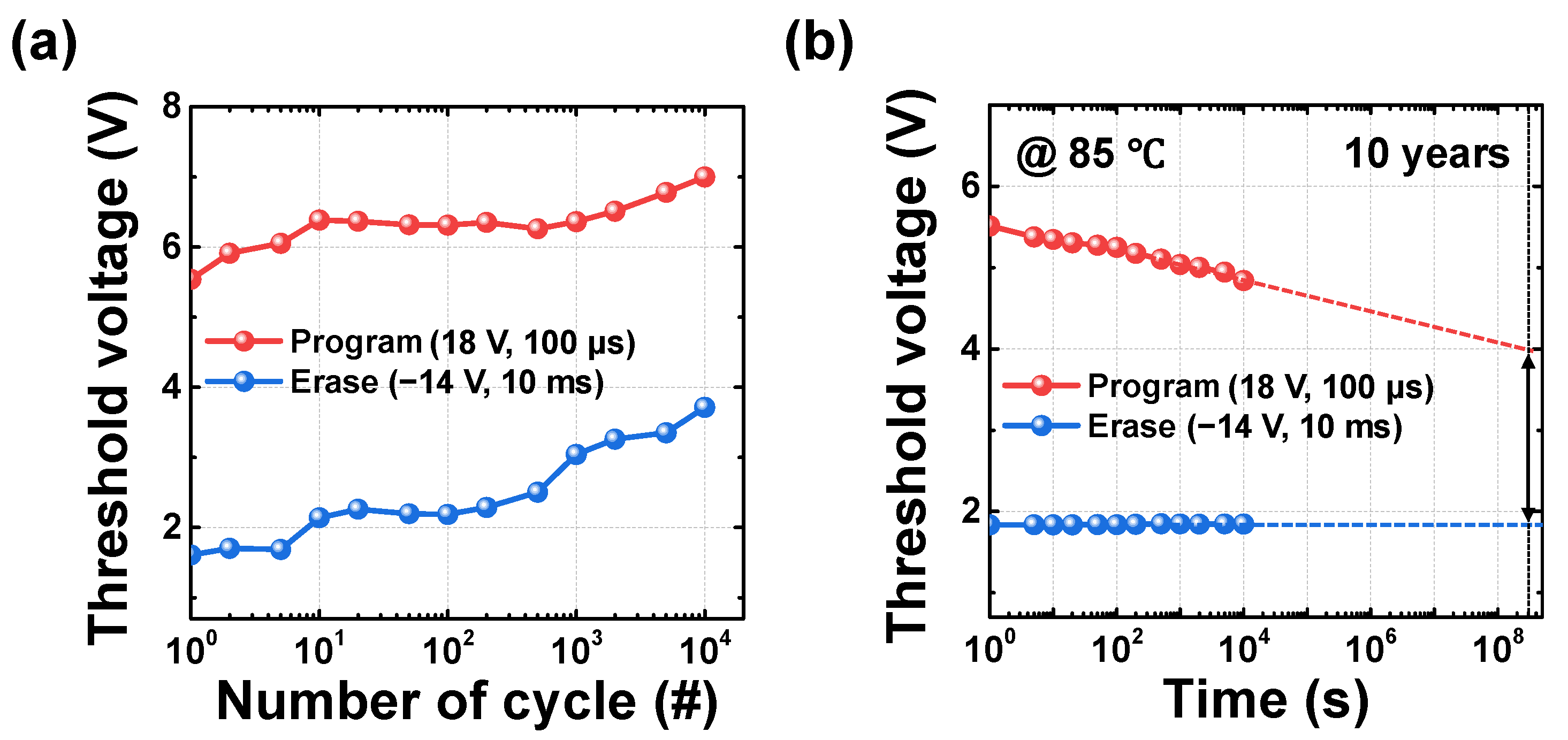
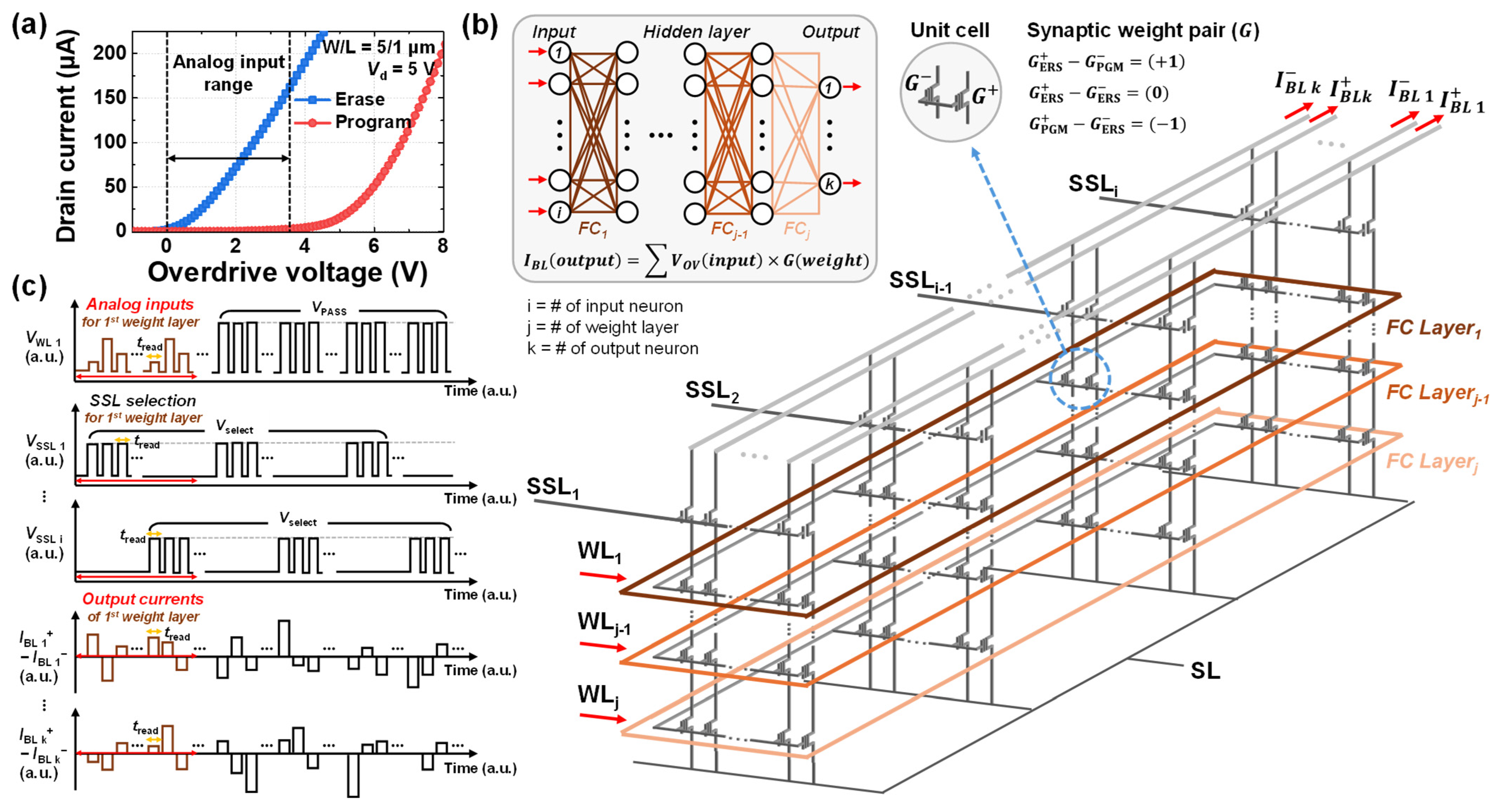
2. Device Fabrication and Electrical Characteristics

Figure 1a shows the process flow of the fabricated NAND flash array, while Figure 1b presents schematic illustrations of each corresponding process step. Initially, a 300 nm-thick buried oxide layer was formed through wet oxidation on a p-type bulk silicon wafer. Then, 100 nm-thick amorphous silicon was deposited at 550 °C using low-pressure chemical vapor deposition (LPCVD). Subsequently, solid-phase crystallization (SPC) was carried out by annealing at 600 °C for 24 h, resulting in the formation of a 100 nm thick poly-Si channel layer. Active area patterning and isolation were then performed through dry etching. Then, 3.8 nm-thick SiO2 tunneling oxide and a 6.3 nm-thick Si3N4 charge trap layer were deposited by LPCVD, followed by the deposition of an 8.9 nm-thick Al2O3 blocking oxide using the atomic layer deposition (ALD). A 50 nm TiN gate electrode was then deposited using metal-organic chemical vapor deposition (MOCVD), followed by the addition of a 25 nm SiO2 hard mask through plasma-enhanced chemical vapor deposition (PECVD) to enhance adhesion between the TiN gate and the photoresist. Gate patterning was followed by etching processes, where the hard mask region was etched using buffered oxide etchant. Subsequently, self-aligned source/drain ion implantation was carried out using As⁺ ions at 40 keV with a dose of 2 × 1015 cm−2, followed by dopant activation via rapid thermal annealing (RTA) at 950 °C for 10 s. Afterward, the BEOL process, including inter-layer dielectric (ILD) deposition, via hole formation, and metallization followed. Finally, forming gas annealing (FGA) was performed at 450 °C for 30 min. Figure 1c shows a cross-sectional transmission electron microscopy (TEM) image of the TANOS gate stack in the fabricated flash device, demonstrating proper layer formation.
The electrical properties of the fabricated device were characterized with a channel width (W) of 5 μm and gate length (L) of 1 μm. The electrical measurements were performed using a Keysight B1500A semiconductor parameter analyzer. The transfer characteristics (Id-Vg) were obtained using the source measure unit (SMU), while write operations of PGM and ERS pulses were applied through the pulse generator unit (PGU). To evaluate the memory characteristics of the fabricated device, incremental step pulse program (ISPP) and incremental step pulse erase (ISPE) methods were employed. Figure 2a presents the measured transfer curves under ISPP operation. For program operation, program voltage (Vpgm) was increased in 0.5 V steps from 9 V to 18.5 V with a pulse width (tpulse) of 100 µs. Conversely, Figure 2b shows the transfer curves under the ISPE operation, where erase voltage (Vers) was decreased in −0.3 V steps from −8 V to −14.3 V with a pulse width of 10 ms. In both operations, the drain voltage (Vd) was set to 0.5 V. Figure 2c shows the device-to-device threshold voltage distributions for the PGM and ERS states measured from 33 devices. For each state, a Vpgm of 18 V with a width of 100 μs and a Vers of −14 V with a width of 10 ms were applied. This confirms that both states follow a Gaussian distribution well.
Figure 3a presents the endurance characteristics over 104 PGM and ERS cycles. A Vpgm of 18 V with a width of 100 μs and a Vers of −14 V with a width of 10 ms were applied, under the same conditions used in Figure 2c. Even after 104 cycles, the device maintains a memory window of approximately 3.28 V, indicating robust endurance performance. Figure 3b illustrates the retention characteristics of the programmed and erased states, evaluated at a temperature of 85 °C. Similar to the endurance measurement, the device was programmed with a Vpgm of 18 V with a pulse width of 100 μs and erased with a Vers of −14 V with a pulse width of 10 ms. The threshold voltage was then measured over time by repeated read operations. After 104 seconds, the threshold voltage of the programmed state decreased from 5.51 V to 4.84 V (a shift of 0.67 V), while the erased state showed shifting from 1.83 V to 1.84 V (a shift of 0.01 V). Extrapolation of the curves using a log-scale plot indicates that the memory window remains greater than 2 V even after 10 years, demonstrating sufficient separation between the two states. These results confirm that the fabricated device exhibits excellent and reliable switching characteristics thanks to the mature technology of flash stack.

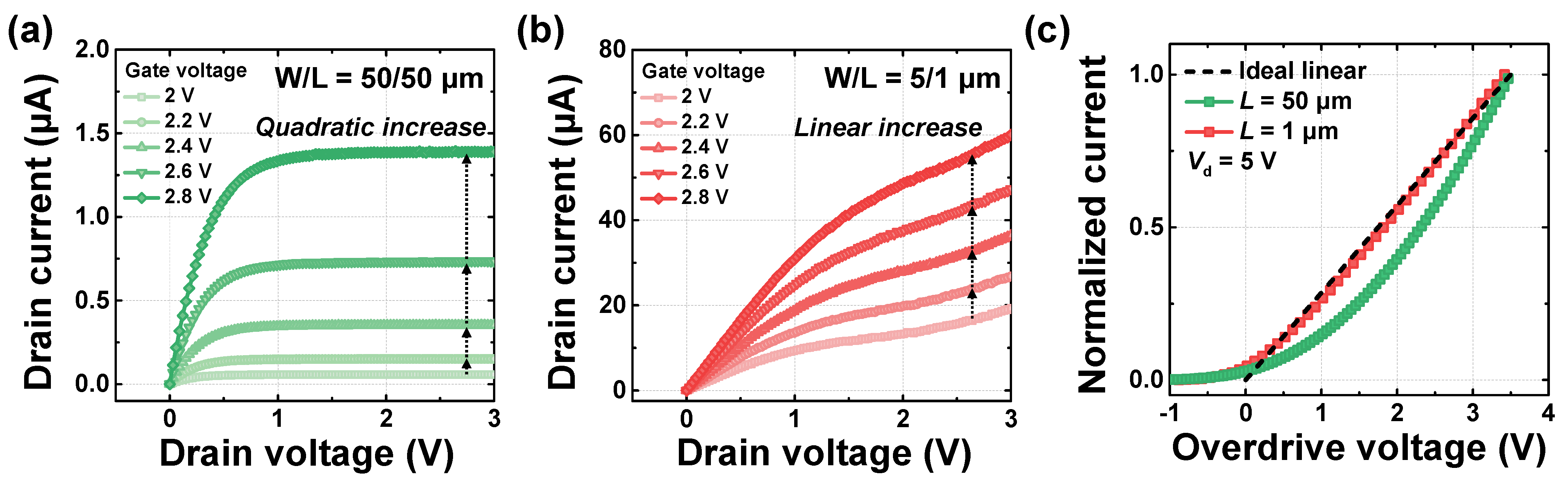
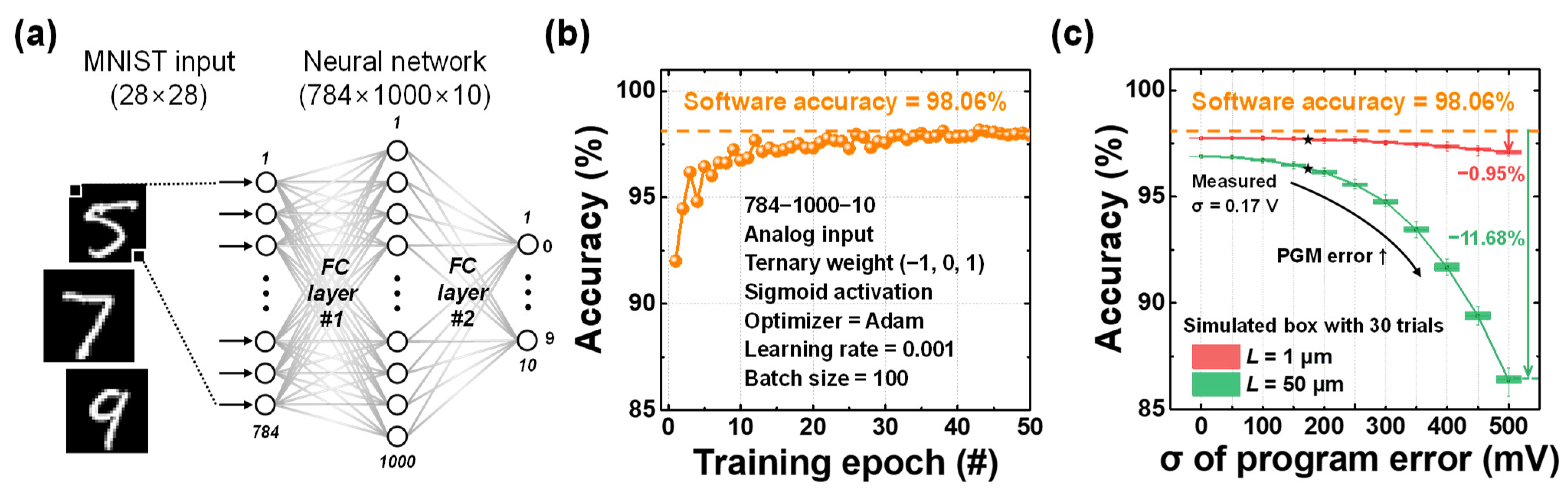
3. Wordline Input Bias Scheme for Neural Network Implementation

Figure 4a,b show the output characteristics of the flash memory devices with L of 50 μm and 1 μm, respectively. This confirms that the increment in drain current with respect to gate voltage becomes linear as velocity saturation occurs because of velocity saturation, for the short channel device. Theoretically, carrier velocity can be expressed as the product of mobility and the electric field applied across the channel. Under these conditions, the resulting drain saturation current is typically approximated as a quadratic function of gate voltage. However, when the electric field increases beyond a specific range, carrier velocity saturates, behaving more like a constant rather than varying with the electric field. This phenomenon causes the relationship between drain current and gate voltage to deviate from a quadratic trend and instead follow a linear relationship. Consequently, the drain saturation current can be approximated as a first-order function of gate voltage. Figure 4c shows the normalized drain current as a function of overdrive voltage (VOV), which is defined as the gate voltage with the threshold voltage subtracted, for both long-channel and short-channel devices, compared against an ideal linear function. To utilize the saturation current, the drain voltage was set to 5 V. As discussed earlier, the long-channel device exhibits a quadratic increase in current, whereas the short-channel device shows a linear increase due to velocity saturation, significantly influencing its response to varying gate voltages. To model this behavior, the region where gate voltage ranged from 0 V to 3.5 V is fitted using a third-order polynomial function for the simulation of 3D-NAND flash array to implement a deep neural network with the WL input bias scheme. This confirms that analog input data can be encoded according to the gate voltage in short-channel devices due to its linear relationship.
Figure 5a shows the Id-VOV characteristics of both the program and erase states of the short-channel device for neuromorphic computing applications. Within the memory window defined by the two states, the erase state exhibits a linear increase in drain current with respect to the gate voltage, which is attributed to velocity saturation. This characteristic enables the use of the memory window region for analog input voltage range. In addition, the device in the erase state operates in the on-current regime, while the program state remains in the subthreshold region, thereby ensuring a large current difference between the two states. This linear IV relationship enables the application of input data as VOV input voltages through the WLs in the 3D-NAND array.
Figure 5b presents the schematic view of the WL input biasing scheme based on the 3D-NAND flash architecture, incorporating the synaptic weight layer. The proposed neuromorphic system performs VMM operations using a weight summation approach based on the following input and output weight configurations: I B L o u t p u t = V O V i n p u t   ×   G ( w e i g h t ) , where IBL represents the BL current, VOV is the input analog WL voltage, and G represents the synaptic weight stored in each cell. Each unit cell consists of two devices, one storing a positive weight value (G+) and the other storing a negative weight value (G). The synaptic weight pair follows the relation G = G + G , where each weight cell is programmed or erased to represent ternary weight states (−1, 0, 1). This configuration allows a single pair of cells to store a weight equivalent to that in the software. Additionally, each FC layer is implemented as a dedicated WL layer, where its corresponding weights of each FC layer are stored. During VMM operation, analog WL voltages are applied to the selected WL layer associated with the active FC layer, while a pass voltage (VPASS) is applied to the remaining WLs to minimize string IR drop and to ensure that computations occur only within the selected layer. The output is then obtained by summing the currents flowing through the BLs. Lastly, the number of SSLs (i) corresponds to the number of input neurons in the input layer, the number of WLs (j) corresponds to the number of FC layers in the neural network model, and the number of paired BLs (k) corresponds to the number of output neurons in the output layer.
Figure 5c illustrates the VMM operation scheme, presenting the pulse diagrams of the applied voltages on the WL1 and SSLs, along with the corresponding BL current responses over time. To obtain the desired product of input values and weights on the BL, only one SSL is activated at a time. This exclusive select operation, which reads the current from a single synaptic pair cell at a time, introduces a drawback in inference latency due to its sequential operation. However, it alleviates the issue of large parasitic capacitance typically found in conventional 3D-NAND flash read operations, which arises from the simultaneous activation of multiple SSLs. In addition, by avoiding the overlap of multiple cell currents, it effectively prevents the accumulation of discrete random telegraph noise-induced fluctuations.
During the first phase of the operation, a select voltage (Vselect) is applied to SSL1 to activate the string select transistor, the first input value X1, encoded as an analog overdrive voltage, is applied to WL1, and the remaining WLs (WL2 to WLj) are biased with VPASS to minimize IR drop and avoid interference in the unselected WL layers. All of these operations are performed simultaneously during a single read pulse (tread). As a result, the corresponding BL pairs generate an output current, representing the product of the input voltage and stored weight. For instance, the sum of the currents from BL1+ and BL1 corresponds to X1 × W11, while the sum of BLk+ and BLk corresponds to X1 × W1k. In the second phase, SSL2 is activated by applying Vselect, and WL1 is biased with the second input value X2, also encoded as voltage, while the remaining WLs continue to bias VPASS. Similar to the first phase, the BLs output currents corresponding to the product of the second input and the weights connected to the second input neuron. Specifically, BLk+ and BLk output X2 × Wk. This process continues iteratively for all n inputs, from SSL1 to SSLi. In this example, a single-layer neural network is considered for demonstration purposes, and all operations are performed on a single WL layer. In the case of multi-layer neural networks, each FC layer is mapped to a corresponding WL layer, and read operations are performed sequentially from the input WL layer to the output WL layer.
A simulation of the MNIST classification task was conducted using a neural network with a 784 × 1000 × 10 architecture, consisting of two FC layers, as illustrated in Figure 6a. The sigmoid function was used as the activation function, and the weights were quantized to ternary values (−1, 0, 1). Quantization-aware training was employed to incorporate weight quantization effects during the training process. The model was trained using the CrossEntropyLoss function and the Adam optimizer with a learning rate of 0.001. A total of 60,000 images were used for training and 20,000 for testing, with training performed over 35 epochs. Figure 6b shows the test accuracy after each epoch using an ideal linear input function, with the accuracy reaching 98.06% at the final epoch. Subsequently, simulations were performed using the fitted Id-VOV transfer curves of the short-channel (L = 1 μm) and long-channel (L = 50 μm) devices, respectively. For both cases, variations in the threshold voltage of the PGM state were applied using a Gaussian distribution with a mean of 0 V and standard deviations ranging from 0 V to 500 mV in 50 mV increments. As shown in Figure 2c, the measured device-to-device threshold variation for the PGM state exhibited a standard deviation of approximately 170 mV. Based on this result, the simulations reflected not only the experimentally extracted variation but also larger potential errors to examine the robustness of the scheme under more severe conditions.
Figure 6c shows the recognition accuracy results, presented as box plots from 30 repeated trials for each case. First, in the case without variation in the PGM state, the recognition accuracy dropped by 1.16% for the long-channel device and by 0.32% for the short-channel device, compared to the ideal linear input function. The relatively larger accuracy drop observed in the long-channel device is attributed to the quadratic characteristic of its IV characteristics. In contrast, although the short-channel device maintained high accuracy, a small drop was still observed. This accuracy drop is attributed to its imperfect linearity compared to the ideal function, as well as the accumulation of residual current due to its inability to fully suppress the current near the zero-input voltage point. Additionally, as the threshold voltage variation of the PGM state increases, the recognition accuracy of the long channel device significantly decreases, by up to 11.68%. This degradation is attributed to the increased shift of the PGM state toward the turn-on region within the memory window between the ERS and PGM states. In this region, although the PGM state is ideally expected to produce zero current, it begins to generate small but non-zero currents relative to the ERS state. As the threshold variation increases, the number of such undesired outputs increases, and the accumulated current eventually affects the overall output, leading to degraded recognition performance. Consequently, the long channel device exhibits a noticeable drop in accuracy. In contrast, despite the presence of such non-idealities, the short channel device shows less than a 1% accuracy drop even under a standard deviation error of 500 mV. This robustness is attributed to its near-perfect linear analog input-output characteristics, which maintain a large current difference between the PGM and ERS states even as program variation increases. As a result, the short-channel device demonstrates strong tolerance to variation and offers the advantage of achieving high accuracy by leveraging analog input behavior.
In addition, in the current implementation, nearly the entire memory window between the PGM and ERS states is used as the input voltage range. However, if the input voltage range is limited to a narrower region within the memory window where the current difference between the PGM and ERS states is very large, the resulting accuracy drop can be reduced. This approach would not only enhance robustness against threshold voltage variation but also improve resilience to other noise sources such as RTN. Moreover, the analog WL input scheme can be effectively applied to short channel devices with channel lengths below approximately 5 μm, as long as they exhibit sufficiently linear IV characteristics, and its effectiveness improves as the channel length decreases due to the increasingly linear behavior [61,62]. In particular, commercially available 3D vertical NAND (VNAND) devices have already been scaled down to below sub-micrometer channel lengths, and even more linear IV characteristics can be achieved compared to the 1 μm channel devices demonstrated in this work [63]. Consequently, such commercialized VNAND is expected to maintain high recognition accuracy and exhibit enhanced robustness against variation. Furthermore, since this approach operates in the saturation region, the drain current exhibits minimal sensitivity to variations in the drain voltage. This characteristic provides tolerance in the output current with respect to fluctuations in the applied drain voltage.

4. Conclusions

We proposed a neuromorphic system based on 3D-NAND flash architecture that utilizes analog input voltages applied through WLs and corresponding BL current outputs. This approach utilized the velocity saturation effect in short-channel MOSFETs in the saturation region, which leads to a near-linear increase in drain current with respect to gate voltage. A NAND flash array utilizing the TANOS gate stack was fabricated, and its electrical characteristics and memory characteristics were evaluated. The output characteristics were experimentally verified to vary with the device channel length. As the channel length decreased, the drain current shifted from a quadratic to a more linear increase with respect to the gate voltage, due to the velocity saturation. By utilizing the linear transfer characteristics, the VOV was used as the input voltage applied through the WLs. Two paired devices represented a single synaptic weight, and each WL layer corresponds to FC layer. The resulting summed BL currents represent the output values. Based on this configuration, we presented a neural network implementation using 3D-NAND flash architecture, along with the voltage biasing scheme required for VMM operations. This methodology overcame the limitations of previous studies, such as the need for additional peripheral circuits to implement multi-bit or analog input signals as well as multi-bit weights and enables the representation of a wider range of analog values with greater flexibility compared to the analog voltages through BLs. Finally, a simulation of MNIST pattern recognition was performed based on the proposed neuromorphic system. The recognition accuracy was evaluated by comparing the cases that reflect the characteristics of long-channel and short-channel devices with that of an ideal linear input function implemented in software. Furthermore, by applying threshold voltage variation in the PGM state, the resulting degradation in recognition accuracy was analyzed. These results demonstrate that the short channel allows for the use of analog inputs with minimal accuracy drop compared to the ideal software-based model while also exhibiting strong robustness against threshold voltage variations, with an accuracy drop under 1% even under worst-case conditions. Moreover, by leveraging the high integration density and technological maturity of 3D-NAND flash arrays, the proposed approach demonstrated strong potential for neuromorphic computing applications.

Author Contributions

Conceptualization, H.K.; methodology, H.H., G.K. and D.Y.; software, G.K.; validation, H.H. and G.K.; writing—original draft preparation, H.H. and G.K.; writing—review and editing, H.K.; supervision, H.K.; funding acquisition, H.K., H.H. and G.K. equally contributed to this work. All authors have read and agreed to the published version of the manuscript.

Funding

This work was supported in part by the NRF funded by the Korean government (RS-2023-00270126, 20%, RS-2025-07402970, 30%), in part by the IITP (Institute for Information & Communications Technology Planning & Evaluation) grant funded by the Korean government (RS-2021-II212052, 20%, RS-2024-00506767, 30%), and in part by the Brain Korea 21 Four Program.

Data Availability Statement

The original contributions presented in the study are included in the article; further inquiries can be directed to the corresponding author/s.

Conflicts of Interest

The authors declare no conflicts of interest.

References

  1. Backus, J. Can programming be liberated from the von Neumann style? A functional style and its algebra of programs. Commun. ACM 1978, 21, 613–641. [Google Scholar] [CrossRef]
  2. Yu, S.; Jiang, H.; Huang, S.; Peng, X.; Lu, A. Compute-in-memory chips for deep learning: Recent trends and prospects. IEEE Circuits Syst. Mag. 2021, 21, 31–56. [Google Scholar] [CrossRef]
  3. Wouters, D.; Brackmann, L.; Jafari, A.; Bengel, C.; Mayahinia, M.; Waser, R.; Menzel, S.; Tahoori, M. Reliability of Computing-In-Memory Concepts Based on Memristive Arrays. In Proceedings of the 2022 International Electron Devices Meeting (IEDM), San Francisco, CA, USA, 3–7 December 2022; pp. 5.3.1–5.3.4. [Google Scholar]
  4. Kim, K.; Song, M.S.; Hwang, H.; Hwang, S.; Kim, H. A comprehensive review of advanced trends: From artificial synapses to neuromorphic systems with consideration of non-ideal effects. Front. Neurosci. 2024, 18, 1279708. [Google Scholar] [CrossRef] [PubMed]
  5. Yu, J.; Lee, G.; Na, T. High-performance Sum Operation with Charge Saving and Sharing Circuit for MRAM-based In-memory Computing. J. Semicond. Technol. Sci. 2024, 24, 111–121. [Google Scholar] [CrossRef]
  6. Chen, L.; Huang, W.; Zhang, K.; Li, B.; Zhang, Z.; Feng, X.; Lin, K.; He, Y.; Zhao, W.; Zhang, Y. Orthogonal-Bulk-Spin-Orbit-Torque Device for All-Electrical In-Memory Computing. IEEE Electron Device Lett. 2024, 45, 504–507. [Google Scholar] [CrossRef]
  7. Liu, N.; Zhou, J.; Zheng, S.; Jin, F.; Fang, C.; Chen, B.; Liu, Y.; Hao, Y.; Han, G. Photoelectric In-memory Logic and Computing Achieved in HfO 2-based Ferroelectric Optoelectronic Memcapacitors. IEEE Electron Device Lett. 2024, 45, 1357–1360. [Google Scholar] [CrossRef]
  8. Wu, B.; Liu, K.; Yu, T.; Zhu, H.; Chen, K.; Yan, C.; Deng, E.; Liu, W. High-performance STT-MRAM-based computing-in-memory scheme utilizing data read feature. IEEE Trans. Nanotechnol. 2023, 22, 817–826. [Google Scholar] [CrossRef]
  9. Kim, C.-K.; Phadke, O.; Kim, T.-H.; Kim, M.-S.; Yu, J.-M.; Yoo, M.-S.; Choi, Y.-K.; Yu, S. Capacitive Synaptor with Overturned Charge Injection for Compute-in-Memory. IEEE Electron Device Lett. 2024, 45, 929–932. [Google Scholar] [CrossRef]
  10. Vasilopoulos, A.; Büchel, J.; Kersting, B.; Lammie, C.; Brew, K.; Choi, S.; Philip, T.; Saulnier, N.; Narayanan, V.; Le Gallo, M. Exploiting the state dependency of conductance variations in memristive devices for accurate in-memory computing. IEEE Trans. Electron Devices 2023, 70, 6279–6285. [Google Scholar] [CrossRef]
  11. Ling, Y.; Wang, Z.; Yu, Z.; Bao, S.; Yang, Y.; Bao, L.; Sun, Y.; Cai, Y.; Huang, R. Temperature-dependent accuracy analysis and resistance temperature correction in RRAM-based in-memory computing. IEEE Trans. Electron Devices 2023, 71, 294–300. [Google Scholar] [CrossRef]
  12. Quesada, E.P.-B.; Mahadevaiah, M.K.; Rizzi, T.; Wen, J.; Ulbricht, M.; Krstic, M.; Wenger, C.; Perez, E. Experimental assessment of multilevel rram-based vector-matrix multiplication operations for in-memory computing. IEEE Trans. Electron Devices 2023, 70, 2009–2014. [Google Scholar] [CrossRef]
  13. Shen, Z.; Zhao, C.; Qi, Y.; Xu, W.; Liu, Y.; Mitrovic, I.Z.; Yang, L.; Zhao, C. Advances of RRAM devices: Resistive switching mechanisms, materials and bionic synaptic application. Nanomaterials 2020, 10, 1437. [Google Scholar] [CrossRef]
  14. Wong, H.-S.P.; Lee, H.-Y.; Yu, S.; Chen, Y.-S.; Wu, Y.; Chen, P.-S.; Lee, B.; Chen, F.T.; Tsai, M.-J. Metal–oxide RRAM. Proc. IEEE 2012, 100, 1951–1970. [Google Scholar] [CrossRef]
  15. Zahoor, F.; Azni Zulkifli, T.Z.; Khanday, F.A. Resistive random access memory (RRAM): An overview of materials, switching mechanism, performance, multilevel cell (MLC) storage, modeling, and applications. Nanoscale Res. Lett. 2020, 15, 90. [Google Scholar] [CrossRef]
  16. Youn, S.; Lee, J.; Kim, S.; Park, J.; Kim, K.; Kim, H. Programmable Threshold Logic Implementations in a Memristor Crossbar Array. Nano Lett. 2024, 24, 3581–3589. [Google Scholar] [CrossRef]
  17. Pan, F.; Gao, S.; Chen, C.; Song, C.; Zeng, F. Recent progress in resistive random access memories: Materials, switching mechanisms, and performance. Mater. Sci. Eng. R-Rep. 2014, 83, 1–59. [Google Scholar] [CrossRef]
  18. Park, J.; Kim, S.; Song, M.S.; Youn, S.; Kim, K.; Kim, T.-H.; Kim, H. Implementation of Convolutional Neural Networks in Memristor Crossbar Arrays with Binary Activation and Weight Quantization. ACS Appl. Mater. Interfaces 2024, 16, 1054–1065. [Google Scholar] [CrossRef]
  19. Duan, S.; Hu, X.; Dong, Z.; Wang, L.; Mazumder, P. Memristor-based cellular nonlinear/neural network: Design, analysis, and applications. IEEE Trans. Neural Netw. Learn. Syst. 2014, 26, 1202–1213. [Google Scholar] [CrossRef]
  20. Kim, T.-H.; Kim, S.; Park, J.; Youn, S.; Kim, H. Memristor Crossbar Array with Enhanced Device Yield for In-Memory Vector–Matrix Multiplication. ACS Appl. Electron. Mater. 2024, 6, 4099–4107. [Google Scholar] [CrossRef]
  21. Akinaga, H.; Shima, H. Resistive random access memory (ReRAM) based on metal oxides. Proc. IEEE 2010, 98, 2237–2251. [Google Scholar] [CrossRef]
  22. Kumar, A.; Krishnaiah, M.; Park, J.; Mishra, D.; Dash, B.; Jo, H.B.; Lee, G.; Youn, S.; Kim, H.; Jin, S.H. Multibit, Lead-Free Cs2SnI6 Resistive Random Access Memory with Self-Compliance for Improved Accuracy in Binary Neural Network Application. Adv. Funct. Mater. 2024, 34, 2310780. [Google Scholar] [CrossRef]
  23. Cai, F.; Correll, J.M.; Lee, S.H.; Lim, Y.; Bothra, V.; Zhang, Z.; Flynn, M.P.; Lu, W.D. A fully integrated reprogrammable memristor–CMOS system for efficient multiply–accumulate operations. Nat. Electron. 2019, 2, 290–299. [Google Scholar] [CrossRef]
  24. Kim, S.; Park, K.; Hong, K.; Kim, T.H.; Park, J.; Youn, S.; Kim, H.; Choi, W.Y. Overshoot-Suppressed Memristor Crossbar Array with High Yield by AlOx Oxidation for Neuromorphic System. Adv. Mater. Technol. 2024, 9, 2400063. [Google Scholar] [CrossRef]
  25. Li, Y.; Wang, Z.; Midya, R.; Xia, Q.; Yang, J.J. Review of memristor devices in neuromorphic computing: Materials sciences and device challenges. J. Phys. D Appl. Phys. 2018, 51, 503002. [Google Scholar] [CrossRef]
  26. Yu, D.; Ahn, S.; Youn, S.; Park, J.; Kim, H. True random number generator using stochastic noise signal of memristor with variation tolerance. Chaos Solitons Fractals 2024, 189, 115708. [Google Scholar] [CrossRef]
  27. Sarwat, S.G.; Kersting, B.; Moraitis, T.; Jonnalagadda, V.P.; Sebastian, A. Phase-change memtransistive synapses for mixed-plasticity neural computations. Nat. Nanotechnol. 2022, 17, 507–513. [Google Scholar] [CrossRef]
  28. Wang, L.; Ma, G.; Yan, S.; Cheng, X.; Miao, X. Reconfigurable Multilevel Storage and Neuromorphic Computing Based on Multilayer Phase-Change Memory. ACS Appl. Mater. Interfaces 2024, 16, 54829–54836. [Google Scholar] [CrossRef]
  29. Chen, X.; Xue, Y.; Sun, Y.; Shen, J.; Song, S.; Zhu, M.; Song, Z.; Cheng, Z.; Zhou, P. Neuromorphic Photonic Memory Devices Using Ultrafast, Non-Volatile Phase-Change Materials. Adv. Mater. 2023, 35, 2203909. [Google Scholar] [CrossRef]
  30. Hamid, S.B.; Khan, A.I.; Zhang, H.; Davydov, A.V.; Pop, E. Low-Energy Spiking Neural Network using Ge4Sb6Te7 Phase Change Memory Synapses. IEEE Electron Device Lett. 2024, 45, 1819–1822. [Google Scholar] [CrossRef]
  31. Kang, Y.G.; Ishii, M.; Park, J.; Shin, U.; Jang, S.; Yoon, S.; Kim, M.; Okazaki, A.; Ito, M.; Nomura, A. Solving Max-Cut Problem Using Spiking Boltzmann Machine Based on Neuromorphic Hardware with Phase Change Memory. Adv. Sci. 2024, 11, 2406433. [Google Scholar] [CrossRef]
  32. Boniardi, M.; Baldo, M.; Allegra, M.; Redaelli, A. Phase Change Memory: A Review on Electrical Behavior and Use in Analog In-Memory-Computing (A-IMC) Applications. Adv. Electron. Mater. 2024, 10, 2400599. [Google Scholar] [CrossRef]
  33. Pistolesi, L.; Ravelli, L.; Glukhov, A.; de Gracia Herranz, A.; Lopez-Vallejo, M.; Carissimi, M.; Pasotti, M.; Rolandi, P.; Redaelli, A.; Martín, I.M. Differential Phase Change Memory (PCM) Cell for Drift-Compensated In-Memory Computing. IEEE Trans. Electron Devices 2024, 71, 7447–7453. [Google Scholar] [CrossRef]
  34. Choi, S.; Kim, S. In-Series Phase-Change Memory Pair for Enhanced Data Retention and Large Window in Automotive Application. IEEE Electron Device Lett. 2024, 45, 2363–2366. [Google Scholar] [CrossRef]
  35. Li, N.; Mackin, C.; Chen, A.; Brew, K.; Philip, T.; Simon, A.; Saraf, I.; Han, J.P.; Sarwat, S.G.; Burr, G.W. Optimization of Projected Phase Change Memory for Analog In-Memory Computing Inference. Adv. Electron. Mater. 2023, 9, 2201190. [Google Scholar] [CrossRef]
  36. Rasch, M.J.; Mackin, C.; Le Gallo, M.; Chen, A.; Fasoli, A.; Odermatt, F.; Li, N.; Nandakumar, S.; Narayanan, P.; Tsai, H. Hardware-aware training for large-scale and diverse deep learning inference workloads using in-memory computing-based accelerators. Nat. Commun. 2023, 14, 5282. [Google Scholar] [CrossRef]
  37. Zhou, Z.; Jiao, L.; Zhou, J.; Zheng, Z.; Chen, Y.; Han, K.; Kang, Y.; Gong, X. Inversion-Type Ferroelectric Capacitive Memory and Its 1-Kbit Crossbar Array. IEEE Trans. Electron Devices 2023, 70, 1641–1647. [Google Scholar] [CrossRef]
  38. Soliman, M.; Maity, K.; Gloppe, A.; Mahmoudi, A.; Ouerghi, A.; Doudin, B.; Kundys, B.; Dayen, J.-F. Photoferroelectric all-van-der-Waals heterostructure for multimode neuromorphic ferroelectric transistors. ACS Appl. Mater. Interfaces 2023, 15, 15732–15744. [Google Scholar] [CrossRef]
  39. Dang, Z.; Guo, F.; Wang, Z.; Jie, W.; Jin, K.; Chai, Y.; Hao, J. Object motion detection enabled by reconfigurable neuromorphic vision sensor under ferroelectric modulation. ACS Nano 2024, 18, 27727–27737. [Google Scholar] [CrossRef]
  40. Xiang, H.; Chien, Y.C.; Li, L.; Zheng, H.; Li, S.; Duong, N.T.; Shi, Y.; Ang, K.W. Enhancing Memory Window Efficiency of Ferroelectric Transistor for Neuromorphic Computing via Two-Dimensional Materials Integration. Adv. Funct. Mater. 2023, 33, 2304657. [Google Scholar] [CrossRef]
  41. Kim, S.; Kim, J.; Kim, D.; Kim, J.; Kim, S. Neuromorphic synaptic applications of HfAlOx-based ferroelectric tunnel junction annealed at high temperatures to achieve high polarization. APL Mater. 2023, 11, 101102. [Google Scholar] [CrossRef]
  42. Koo, R.H.; Shin, W.; Kim, J.; Yim, J.; Ko, J.; Jung, G.; Im, J.; Park, S.H.; Kim, J.J.; Cheema, S.S. Polarization Pruning: Reliability Enhancement of Hafnia-Based Ferroelectric Devices for Memory and Neuromorphic Computing. Adv. Sci. 2024, 11, 2407729. [Google Scholar] [CrossRef]
  43. Li, Z.; Meng, J.; Yu, J.; Liu, Y.; Wang, T.; Liu, P.; Chen, S.; Zhu, H.; Sun, Q.; Zhang, D.W. CMOS compatible low power consumption ferroelectric synapse for neuromorphic computing. IEEE Electron Device Lett. 2023, 44, 532–535. [Google Scholar] [CrossRef]
  44. Huang, W.-Y.; Nie, L.-H.; Lai, X.-C.; Fang, J.-L.; Chen, Z.-L.; Chen, J.-Y.; Jiang, Y.-P.; Tang, X.-G. Synaptic Properties of a PbHfO3 Ferroelectric Memristor for Neuromorphic Computing. ACS Appl. Mater. Interfaces 2024, 16, 23615–23624. [Google Scholar] [CrossRef]
  45. Gao, J.; Chien, Y.C.; Li, L.; Lee, H.K.; Samanta, S.; Varghese, B.; Xiang, H.; Li, M.; Liu, C.; Zhu, Y. Ferroelectric Aluminum Scandium Nitride Transistors with Intrinsic Switching Characteristics and Artificial Synaptic Functions for Neuromorphic Computing. Small 2024, 20, 2404711. [Google Scholar] [CrossRef]
  46. Lu, T.; Zhao, X.; Liu, H.; Yan, Z.; Zhao, R.; Shao, M.; Yan, J.; Yang, M.; Yang, Y.; Ren, T.-L. Optimal Weight Models for Ferroelectric Synapses Toward Neuromorphic Computing. IEEE Trans. Electron Devices 2023, 70, 2297–2303. [Google Scholar] [CrossRef]
  47. Lee, S.-T.; Lee, J.-H. Review of neuromorphic computing based on NAND flash memory. Nanoscale Horiz. 2024, 9, 1475–1492. [Google Scholar] [CrossRef]
  48. Kim, J.P.; Kim, S.K.; Park, S.; Kuk, S.-H.; Kim, T.; Kim, B.H.; Ahn, S.-H.; Cho, Y.-H.; Jeong, Y.; Choi, S.-Y. Dielectric-engineered high-speed, low-power, highly reliable charge trap flash-based synaptic device for neuromorphic computing beyond inference. Nano Lett. 2023, 23, 451–461. [Google Scholar] [CrossRef]
  49. Park, E.; Jang, S.; Noh, G.; Jo, Y.; Lee, D.K.; Kim, I.S.; Song, H.-C.; Kim, S.; Kwak, J.Y. Indium–Gallium–Zinc Oxide-Based Synaptic Charge Trap Flash for Spiking Neural Network-Restricted Boltzmann Machine. Nano Lett. 2023, 23, 9626–9633. [Google Scholar] [CrossRef]
  50. Hwang, S.; Yu, J.; Song, M.S.; Hwang, H.; Kim, H. Memcapacitor crossbar array with charge trap NAND flash structure for neuromorphic computing. Adv. Sci. 2023, 10, 2303817. [Google Scholar] [CrossRef]
  51. Zhu, A.; Jin, L.; Jia, J.; Ye, T.; Zeng, M.; Huo, Z. HCMS: A Hybrid Conductance Modulation Scheme Based on Cell-to-Cell Z-Interference for 3D NAND Neuromorphic Computing. IEEE J. Electron Devices Soc. 2024. [Google Scholar] [CrossRef]
  52. Xiang, Y.; Huang, P.; Han, R.; Li, C.; Wang, K.; Liu, X.; Kang, J. Efficient and robust spike-driven deep convolutional neural networks based on NOR flash computing array. IEEE Trans. Electron Devices 2020, 67, 2329–2335. [Google Scholar] [CrossRef]
  53. Feng, Y.; Tang, M.; Sun, Z.; Qi, Y.; Zhan, X.; Liu, J.; Zhang, J.; Wu, J.; Chen, J. Fully flash-based reservoir computing network with low power and rich states. IEEE Trans. Electron Devices 2023, 70, 4972–4975. [Google Scholar] [CrossRef]
  54. Wang, H.; Lu, Y.; Liu, S.; Yu, J.; Hu, M.; Li, S.; Yang, R.; Watanabe, K.; Taniguchi, T.; Ma, Y. Adaptive Neural Activation and Neuromorphic Processing via Drain-Injection Threshold-Switching Float Gate Transistor Memory. Adv. Mater. 2023, 35, 2309099. [Google Scholar] [CrossRef]
  55. Hwang, H.; Song, M.S.; Youn, S.; Kim, H. True Random Number Generator using Memcapacitor with Charge Trapping Layer. IEEE Electron Device Lett. 2024, 45, 1464–1467. [Google Scholar] [CrossRef]
  56. Ansari, M.H.R.; El-Atab, N. Efficient Implementation of Boolean Logic Functions Using Double Gate Charge-Trapping Memory for In-Memory Computing. IEEE Trans. Electron Devices 2024, 71, 1879–1885. [Google Scholar] [CrossRef]
  57. Wang, P.; Xu, F.; Wang, B.; Gao, B.; Wu, H.; Qian, H.; Yu, S. Three-dimensional NAND flash for vector–matrix multiplication. IEEE Trans. Very Large Scale Integr. (VLSI) Syst. 2018, 27, 988–991. [Google Scholar] [CrossRef]
  58. Lee, S.-T.; Lim, S.; Choi, N.Y.; Bae, J.-H.; Kwon, D.; Park, B.-G.; Lee, J.-H. Operation scheme of multi-layer neural networks using NAND flash memory as high-density synaptic devices. IEEE J. Electron Devices Soc. 2019, 7, 1085–1093. [Google Scholar] [CrossRef]
  59. Lue, H.-T.; Hsu, P.-K.; Wei, M.-L.; Yeh, T.-H.; Du, P.-Y.; Chen, W.-C.; Wang, K.-C.; Lu, C.-Y. Optimal design methods to transform 3D NAND flash into a high-density, high-bandwidth and low-power nonvolatile computing in memory (nvCIM) accelerator for deep-learning neural networks (DNN). In Proceedings of the 2019 IEEE International Electron Devices Meeting (IEDM), San Francisco, CA, USA, 7–11 December 2019; pp. 38.31.31–38.31.34. [Google Scholar]
  60. Lee, S.-T.; Lee, J.-H. Neuromorphic computing using NAND flash memory architecture with pulse width modulation scheme. Front. Neurosci. 2020, 14, 571292. [Google Scholar] [CrossRef]
  61. Sodini, C.G.; Ko, P.-K.; Moll, J.L. The effect of high fields on MOS device and circuit performance. IEEE Trans. Electron Devices 1984, 31, 1386–1393. [Google Scholar] [CrossRef]
  62. Duvvury, C. A guide to short-channel effects in MOSFETs. IEEE Circuits Devices Mag. 1986, 2, 6–10. [Google Scholar] [CrossRef]
  63. Tanaka, H.; Kido, M.; Yahashi, K.; Oomura, M.; Katsumata, R.; Kito, M.; Fukuzumi, Y.; Sato, M.; Nagata, Y.; Matsuoka, Y.; et al. Bit Cost Scalable technology with Punch and plug process for ultra high density flash memory. In Proceedings of the 2007 IEEE Symposium on VLSI Technology, Kyoto, Japan, 12–14 June 2007; pp. 14–15. [Google Scholar]
Figure 1. Fabrication of NAND flash array with TANOS stack. (a) Process flow of the fabricated NAND flash device. (b) Schematic diagram for each process step. (c) Cross-sectional TEM image of TANOS gate stack.
Biomimetics 10 00318 g001
Figure 2. Electrical characteristics of the fabricated device. (a) Measured Id-Vg transfer characteristics with ISPP scheme. (b) Measured Id-Vg transfer characteristics with ISPE scheme. (c) Threshold voltage distributions of PGM and ERS states measured from 33 devices.
Biomimetics 10 00318 g002
Figure 3. Memory characteristics. (a) Endurance characteristics for 104 cycles. (b) Retention characteristics measured at 85 °C.
Biomimetics 10 00318 g003
Figure 4. Output characteristics with varying the gate voltage (a) for long-channel device (W/L = 50/50 μm) and (b) short-channel device (W/L = 5/1 μm). (c) Comparison of the normalized currents of the long-channel and short-channel devices with an ideal linear function, with respect to overdrive voltage.
Biomimetics 10 00318 g004
Figure 5. (a) Id-VOV characteristics for both program and erase states, along with the corresponding analog input voltage range. (b) Schematic view of a 3D-NAND flash array implementing an artificial neural network with an analog WL input bias scheme. (c) Operation pulse diagram of WL1, SSLs, and BLs over time.
Biomimetics 10 00318 g005
Figure 6. (a) Schematic of a neural network for MNIST pattern recognition, consisting of two FC layers with sigmoid activation functions. (b) Software training results using analog input, ternary weights, and sigmoid activation functions. (c) Thirty-trial box plot of training results utilizing the analog Id-VOV characteristics of short-channel and long-channel devices along with the program error.
Biomimetics 10 00318 g006
Disclaimer/Publisher’s Note: The statements, opinions and data contained in all publications are solely those of the individual author(s) and contributor(s) and not of MDPI and/or the editor(s). MDPI and/or the editor(s) disclaim responsibility for any injury to people or property resulting from any ideas, methods, instructions or products referred to in the content.

