1. Introduction
In the last few years, both Convolutional and Deconvolutional Neural Networks (CNNs and DCNNs) have been extensively used in deep-learning applications, such as object generation [
1], image segmentation [
2] and high-resolution imaging [
3]. In such a scenario, while deconvolutions aim at extrapolating new features from inputs, to furnish upsampled outputs, convolutions compact the most relevant features through a downsampling process. Despite this difference, the operations are performed in a similar way. Deconvolutions, in fact, can be thought as convolutions executed on padded and strided inputs [
4]. It represents the backbone of segmentation and super-resolution algorithms and it constitutes the basis of generative neural networks, successfully adopted to: synthesize realistic photographs or cartoons; perform images translation tasks; predict future frames in video sequences.
In typical deep-learning applications, owing to the huge amount of Multiply Accumulations (MACs) needed to perform convolutions and deconvolutions, the overall computational complexity can become an issue, especially when operating in real time is mandatory [
5]. The bottleneck introduced by these operations is even more emphasized when software-based designs are implemented by Central Processing Units (CPUs), which provide limited parallelism. Conversely, as is well known, the use of Graphics Processing Units (GPUs) certainly can alleviate performance issues, but, unfortunately, they are not suitable for energy-constrained environments. Indeed, the latter can take advantages from Application-Specific Integrated Circuits (ASICs) and Field-Programmable Gate Arrays (FPGAs) that are widely recognized as appropriate hardware platforms to trade-off performance and power efficiency [
6]. As a further advantage, FPGA-based designs also ensure flexibility and low costs to be achieved. However, although, as exhaustively reviewed in [
7], plenty of FPGA-based accelerators can be found in the literature for CNNs, existing works focusing on the design of FPGA-based engines suitable for hardware-accelerating DCNNs are still few [
8,
9,
10,
11,
12,
13,
14,
15,
16,
17,
18] and this problem is still open.
This paper presents a novel purpose-designed custom hardware accelerator to perform deconvolutions efficiently. The proposed Deconvolution Layer Processing Element (DLPE) was designed with embedded capability, to be easily integrated within virtually any heterogeneous FPGA-based System-on-Chip (SoC). Such a design approach was selected since it is effective in boosting performance and trading off power consumption and costs [
19]. In fact, it merges the powerfulness of a dedicated Processing System (PS), suitable for control and non-time critical tasks, and the flexibility of a Programmable Logic (PL) fabric that can host hardware accelerators purposely designed for computationally intensive operations, such as convolutions and deconvolutions.
The FPGA-based hardware structure proposed here to speed up deconvolutions has been designed with a wide variety of applications in mind. Therefore, the main objectives have been: (1) achieving high-speed performance; (2) limiting the hardware resources requirements and the power consumption; and (3) making the accelerator easily scalable to comply with resources available within both high- and low-end FPGA-based SoCs. As demonstrated in the following, the novel accelerator satisfies all the above goals not only by smartly using logic and routing resources, but also by adopting an efficient data transfer policy to read and write data from/to an external memory. The proposed design complies with the Advanced eXtensible Interface (AXI4) protocol [
20] and, therefore, it can be easily integrated within modern heterogeneous embedded systems.
As a case study, the novel engine has been employed to accelerate Deep Convolutional Generative Adversarial Networks (DCGANs) [
21]. Such a kind of applications could certainly benefit from the latest advanced highly integrated hardware/software platforms, such as the Xilinx’s Versal™ Adaptive Compute Acceleration Platform (ACAP), very recently presented in [
22]. However, for purposes of comparison with state-of-art competitors, the Xilinx Zynq XC7Z020 (Xilinx, San Jose, CA, USA), XC7Z045 (Xilinx), XC7Z100 (Xilinx) [
23] and the Virtex-7 XC7VX690T (Xilinx) [
24] devices have been used as the implementation platforms to characterize the proposed accelerator when running either as a Standalone Unit (SU) or as a part of an Embedded System (ES). When compared to the designs presented in [
9,
11,
15,
16,
17,
18], both the SU and the ES implementations proposed here exhibit remarkably higher throughput and they employ significantly lower amounts of Look-Up Tables (LUTs), Flip-Flops (FFs), on-chip Blocks of Random Access Memory (BRAMs), and Digital Signal Processors (DSPs). As an example, when implemented within the XC7Z020 device, the proposed ES is 50% faster than [
9], performs ~20.7× more GOPs, and it occupies 49.8%, 42.7%, 36.6% and 5% less LUTs, FFs, BRAMs, and DSPs, respectively, dissipating just 1.73 W@150 MHz.
Ultimately, the main contributions and novelties provided in this work can be summarized as follows:
an easily scalable engine for deconvolution is proposed that can be fruitfully employed within different CNNs/DCNNs models;
the novel architecture exploits both data- and circuit-level parallelism, thus it is suitable for accelerating deconvolutions within both high- and low-end FPGA-based SoCs;
the on-chip DSPs resources are fully exploited to perform both multiplication and addition operations, therefore speed performance higher than the state-of-the art competitors is achieved with reduced logic resources requirements and power consumption;
the proposed hardware accelerator complies with the Advanced eXtensible Interface (AXI4) protocol [
20] and, therefore, it can be easily integrated within modern heterogeneous embedded systems;
input and output data streams are read and written from/to an external memory through the raster-order transfer policy; the latter allows data packets to be moved concurrently, thus improving the global latency.
The rest of the paper is organized as follows:
Section 2 provides a background on deconvolution algorithms and related works concerning FPGA-based accelerators;
Section 3 describes the architecture of the proposed hardware accelerator; tests and results are discussed in
Section 4; finally, in
Section 5, conclusions are drawn.
2. Background, Related Works, and Motivations
Representative examples of CNN and DCNN models requiring deconvolutions are provided by the Fully Convolutional Network (FCN) described in [
25], the U-Net architecture presented in [
26], the Super-Resolution CNN (SRCNN) discussed in [
3], and the generative DCNNs demonstrated in [
21]. By examining those network models, it can be easily observed that although a CNN consists of cascaded convolutional layers (CONVs), a DCNN comprises a certain number of cascaded deconvolutional layers (DECONVs). In both cases, cascaded layers are interleaved by optional stages, such as non-linearity, normalization, pooling [
5] and unpooling [
27]. To meet a precise task, such as classification and segmentation, along the whole architecture of a CNN, each CONV extracts even more abstract features from 2D input feature maps (
ifmaps). Moreover, different bottom layers concur to dictate the target of each model. As an example, while classification networks adopt fully connected layers to arrange extracted features in categories, segmented images are built by means of up-sampling stages, including DECONVs [
28]. This means that performing deconvolutions efficiently provides benefits not only to DCNNs, but also to a certain class of CNNs.
Generally speaking, a DECONV layer receives a set of NC 2D H × W ifmaps and produces NF 2D Ho × Wo output feature maps (ofmaps). To do this, NF sets of NC 2D K × K filters kernels are used. More precisely, each ifmap is filtered by using its own kernel and the NC results obtained in this way are combined by means of a pixel-wise addition, thus providing an ofmap. This mechanism is repeated for all the NF sets of filters. Ultimately, it can be said that at the top-level, DECONVs act quite similarly to CONVs. However, when the bare deconvolution and convolution operations are examined, significant differences become more or less evident, depending on the computational strategy adopted within DECONVs.
The method adopted in [
4] computes deconvolutions by executing typical convolutions on zero-padded and strided
ifmaps. More exactly, with
K,
S, and
P being the kernel size, the stride, and the padding, respectively, the deconvolution result is obtained by interleaving
S − 1 zeros between each pair of consecutive input pixels and then performing the classical convolution operation adopting the kernel size
K’ =
K, the stride
S’ = 1, and the padding
P’ =
K −
P − 1. As an example, such a strategy is exploited in the FlexiGAN framework presented in [
8] to generate accelerators for Generative Adversarial Networks (GANs). Unfortunately, this approach requires data and filter be properly reorganized thus making additional control logic necessary and severely limiting the achievable overall performance. As a further drawback, the above-described zero-padding and striding strategies lead to unbalanced workloads since they introduce useless zeroed MAC operations.
The efficient design strategy recently presented in [
17] overcomes the above issues by performing a kernel conversion to calculate all the pre-addable weight combinations. The output of this process is a new set of filters that can be directly applied to the
ifmaps to perform a traditional 3D convolution. Such a strategy allows drastically reducing the computational complexity and introduces remarkable speed-up either over other FPGA accelerators or over GPU platforms.
A completely different technique has been recently proposed in [
9]. Such an approach multiplies each input pixel by the relative
K × K deconvolution kernel, thus furnishing a block of
K × K output products. It is worth noting that neighboring input pixels lead to overlapping output blocks. With
S being the supported stride, up to
K −
S overlapping rows and columns must be properly managed to provide the correct deconvolution result. Unfortunately, the Deconvolution Engine (DE) proposed in [
9] does not manage overlaps efficiently. In fact, to recognize no-overlapping blocks, it applies the reverse looping that requires the computation of input coordinates at each filtering step, with obvious penalties in terms of computational complexity and delay.
Appreciable improvements were introduced in [
10,
11,
12,
13,
14,
15,
16,
18]. The accelerator proposed in [
10] was purposely designed to accomplish the semantic segmentation. It uses separate convolution and deconvolution engines, but, due to its hardware resources requirements, it is not easily exploitable within low-end FPGA-based SoCs. Moreover, while multiplications are performed as fast as possible, by exclusively exploiting DSP slices, the additions required to proper manage overlapping rows/columns are performed through configurable logic resources, thus severely limiting the achievable performance. As a further drawback is that the accelerator does not support the final cropping. Therefore, as demonstrated in [
11], auxiliary logic modules must be introduced to crop pixels on the borders around the
ofmaps.
The above-described structure was further improved in [
12], where a unique engine is used to perform both convolutions and deconvolutions to meet the remote segmentation task. Such an accelerator employs just one MAC unit that operates in a serial manner, whereas it exploits a high level of parallelism at both
fmaps and filters levels. Unfortunately, due to its high hardware resources requirements, this accelerator can be actually exploited only within high-end FPGA-based SoCs. Moreover, it is not the most attractive solution for achieving the highest speed. In fact, it requires up to 4 clock cycles to furnish each deconvolved pixel, depending on how many overlapping pixels must be managed [
12].
The innovative solutions proposed in [
13,
14] avoid the use of dedicated deconvolution engines by transforming deconvolutional layers into convolutional ones. In such a case,
NF × S ofmaps are provided instead of just
NF, thus making a very high parallelism level necessary to achieve reasonable speed performance. Consequently, once again, the resulting hardware resources requirement makes the use of a high-end FPGA device necessary.
Although all the previous works faced the acceleration of 2D deconvolutions, the solution proposed in [
15] is suitable also for 3D scenarios. It exploits the sparsity of input activations and weights to reduce the number of useless multiplications, introducing a compression scheme that further enhances the efficiency of the computational unit. However, the approach presented in [
15] requires non-zero weights to be encoded in coordinate format. This task involves the calculation of the output coordinates of each deconvolved pixel, thus preventing the integration of such an accelerator in streaming-based heterogeneous embedded systems.
As demonstrated in [
16,
18], also the well-known Winograd algorithm can be exploited to deploy deconvolutional layers of GANs on FPGAs efficiently. Indeed, the Winograd algorithm transforms 2D convolutions into element-wise multiplications implemented by simple additions and shifts operations. Despite the impressive speed performance achieved in [
16,
18] also thanks to the high parallelism adopted, this computational method introduces area and power overheads due to the pre- and post-processing operations required to transform feature maps and filters in the Winograd domain.
3. The Proposed Hardware Accelerator
The approach adopted here to deconvolve one
H × W ifmap by a
K × K kernel with stride
S consists of four main steps. In the first one, the generic input pixel
I(
i,
j) is multiplied by the kernel and the resulting block of
K × K products is properly arranged within the
ofmap by occupying the
K × K area starting at the position (
I × S, j × S). As expected, neighboring resulting blocks, obtained from neighboring input pixels, have up to
K–S overlapping rows/columns, which are summed up in the second step. Then, the above steps are repeated for all the input pixels. Finally,
P pixels on the borders around the resulting
ofmap are cropped, thus generating a
H0 ×
W0 ofmap, with
H0 and
W0 being defined in Equation (1).
The example depicted in
Figure 1 shows how this approach deconvolves a 3 × 3
ifmap by using
K = 3,
S = 2 and
P = 1. When deconvolved by the referred 3 × 3 kernel, the orange pixel
I(0,0) in the
ifmap leads to the orange 3 × 3 block of pixels starting at the location (0,0) in the intermediate
ofmap. Similarly, by deconvolving the red pixel
I(1,1) in the
ifmap, the 3 × 3 red block starting at the location (2,2) in the intermediate
ofmap is obtained. In addition, so on for all the other pixels. To complete the deconvolution correctly, the overlapping pixels within neighboring blocks in the
ofmap are summed up. Finally, since
P = 1, one pixel is cropped on the borders around the
ofmap, as highlighted in grey.
The top-level architecture of the novel accelerator, hereby named DLPE, is depicted in
Figure 2. It can process
TN ifmaps (
if0,…,
ifTN−1) and
TM kernels in parallel, thus operating on
TM ofmaps (
of0,…,
ofTM−1) at the same time. In particular, the DLPE can receive
PN pixels from each
ifmap and can furnish
PM elements for each
ofmap contemporaneously, with
PM = S × S × PN. Obviously,
TN,
TM,
PN, and PM strictly depend on the resources availability within the specific device chosen as the realization platform. Anyway, when the number
NC of
ifmaps and/or the number
NF of kernels to be processed are greater than
TN and
TM, respectively, the overall computation is completed within multiple steps, as discussed in the following.
The top-level architecture of the novel accelerator, hereby named DLPE, is depicted in
Figure 2. It can process
TN ifmaps (
if0,…,
ifTN−1) and
TM kernels in parallel, thus operating on
TM ofmaps (
of0,…,
ofTM −1) at the same time. In particular, the DLPE can receive
PN pixels from each
ifmap and can furnish
PM elements for each
ofmap contemporaneously, with
PM = S × S × PN. Obviously,
TN,
TM,
PN, and PM strictly depend on the resources availability within the specific device chosen as the realization platform. Anyway, when the number
NC of
ifmaps and/or the number
NF of kernels to be processed are greater than
TN and
TM, respectively, the overall computation is completed within multiple steps, as discussed in the following.
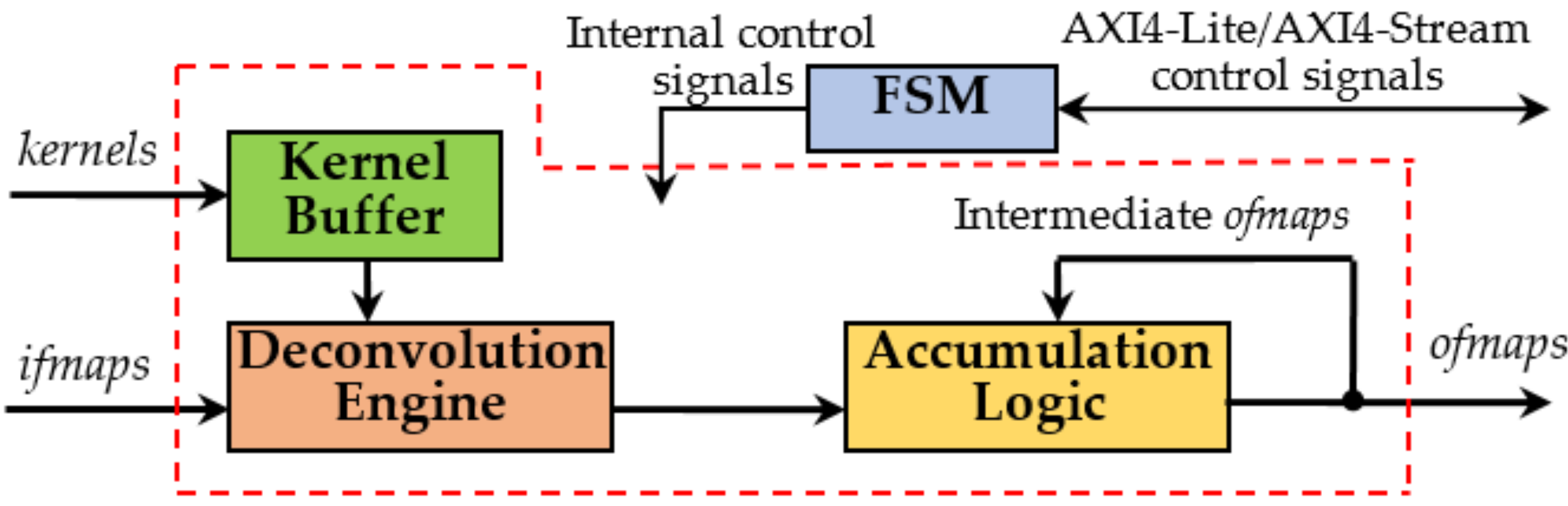
The novel accelerator has been designed supposing that both
ifmaps and kernels are stored within an external Double Data Rate (DDR) memory and, as shown later, they can be simply uploaded and streamed towards the DLPE by auxiliary circuitries, such as Direct Memory Access (DMA) and/or Video DMA (VDMA) modules. Although the
F-bit pixels of the
ifmaps are streamed-in directly to the DE, the
N-bit kernels coefficients are preliminarily locally stored within the Kernel Buffer and then provided to the DE at the proper time. The Accumulation Logic (AL) exploits fast adder trees to accumulate provisional results produced at the various computational steps and collected within on-chip memory resources until the last step is performed and the final
ofmaps are generated. The Finite State Machine (FSM) orchestrates all the operations and makes the whole accelerator AXI4 [
20] compliant. In fact, it takes care of managing all the activities related to data transfers, including the AXI4-Stream transactions through which the packed kernels coefficients and the
ifmaps are received.
The Kernel Buffer, shown in
Figure 3, mainly consists of a register file able to store
K × K × TM × TN N-bit coefficients. At each clock cycle, the buffer receives the homologous coefficients related to the
TN ifmaps if0, …,
ifTN−1 and packed within one
TN × N-bit word. This strategy allows uploading all the kernel coefficients processed in parallel by the DE within just
K × K × TM clock cycles. The Separate and Route logic properly dispatches the coefficients to the DE. The latter is the computational core of the proposed DLPE and, as illustrated in
Figure 4, it consists of
TM × TN Deconvolution Units (DUs) operating in parallel. At each clock cycle, the generic
receives
PN adjacent input pixels
I(
i,j),
I(
i,j + 1), …,
I(
i,j +
PN − 1) from the
ifmap ifin, with
in = 0, …,
TN − 1, and deconvolves them with the relative
K × K kernel
as required to compute the
ofmap ofout, with
out = 0, …,
TM – 1. The input pixels are multiplied in parallel by the coefficients of the kernel and
PN blocks of
K ×
K products are computed contemporaneously.
Each DU was structured as depicted in
Figure 5 to manage efficiently the overlapping rows/columns between these neighboring blocks of products.
Figure 5 shows that the generic DU consists of the
K modules Row
x, with
x = 0, …,
K − 1, each using an appropriate number of DSPs, depending on the supported parallelism level. Furthermore, to guarantee the proper time alignment of the overlapping products, First-In-First-Out (FIFO) Buffers are exploited.
To better explain how the generic DU performs deconvolutions, let us consider, as an example, the kernel size
K = 5, the stride
S = 2 and
PN = 4. In this case,
x ranges from 0 to 4 and five modules Row
x are required, each one, as reported in
Figure 6, consisting of 20 DSPs. The latter are named
dy, with
d = 0, …, 3 and
y ranging from 0 to 4, to indicate that they multiply the input pixel
I(
i,j +
d) by the kernel coefficient
C(x,y). The additional DSPs
x0, …,
x7 are required only within the modules Row0, Row1, and Row2 to manage the overlapping rows. On the contrary, the
S ×
PN results computed by Row3 and Row4 are directly provided by the DSPs 00, 01, 10, 11, 20, 21, 30, and 31. All the multiplications and the additions performed in the examined example by the generic DU are summarized in
Figure 7 that also shows, for each entry, the related row and column indices within the intermediate
ofmap currently computed. Since
K – S = 3, as highlighted by colored entries, each block of products computed by the DU has three columns and three rows overlapped with neighboring blocks.
It is easy to observe that several kinds of overlapping products must be managed. The products related to the
PN adjacent input pixels, currently received by the DU, have the row index equal to
i and the column index ranging between
j and
j + 3. These products are reported in
Figure 7 with black characters and their overlaps are managed through the red interconnections visible in
Figure 6. Conversely, the products reported in
Figure 7 with red characters are being computed at the next clock cycle, when the DU is receiving the next
PN adjacent pixels, i.e.,
I(
i,j + 4), …,
I(
i,j + 7), as input. The column overlaps related to these products are managed through the blue interconnections used in
Figure 6 to transfer the delayed outputs produced by the DSPs 32, 33 and 34 towards the DSPs 00, 01, and 02, respectively. Finally, the products reported in
Figure 7 with blue characters involve the pixels
I(
i + 1,
j), …,
I(
i + 1,
j + 3), which belong to the (
i + 1)-th row of the
ifmap currently processed. To receive these pixels as input, the DU must wait for all the pixels of the
i-th row have been processed. As above illustrated in
Figure 5, to guarantee the proper time alignment of these overlapping products, appropriate Buffers are exploited. In the examined example, they are required at the output of the three modules Row2, Row3, and Row4. These overlapping products are managed within the modules Row0, Row1 and Row2 through the DSPs
x0, …,
x7 and the green interconnections depicted in
Figure 6. Thanks to the fully pipelined adopted architecture, after the initial latency, each DU furnishes
S × S × PN deconvolved pixels at every clock cycle. These deconvolved pixels are reported in the white entries of
Figure 7 as provided by the modules Row0 and Row1.
Obviously, resources requirements, latency and throughput rate of the DE depend on the ifmaps size H × W, as well as on K, S, TN, TM, and PN. In the generic scenario, each DU needs [K × K + S × (K − S)] × PN DSP slices to perform multiplications and to sum the overlapping neighboring products that are time aligned through S × (K – S) × PN row buffers, each being depth.
The novel DE has been designed taking into account also the treatment of border pixels. This is a key aspect, since it affects the data flow of the input streams. In fact, each of the TM × TN DUs operating in parallel receives its own ifmap in the raster order. At the end of each row, the DE stops the incoming stream of pixels for clock cycles. During this time, the zero-padding is applied through a proper multiplexing logic directly controlled by the FSM that also manages the AXI4 protocol signals coherently with the desired wait. At the end of the current step, the DE provides padding rows, before acquiring the next group of ifmaps to perform the subsequent computational step.
As above explained, each of the parallel DUs inside the DE outputs
TM ×
TN blocks of
S × S × PN deconvolved pixels. The homologous pixels within these blocks are accumulated to compose an intermediate
ofmap. In turn, the intermediate
ofmaps are accumulated step-by-step to each other until the DLPE provides the final result. The AL purposely designed to operate in this way is depicted in
Figure 8a. The Route module receives blocks of deconvolved pixels from the DUs and sends them to
S × S × TM × PN adder trees taking into account that each group of
TN homologous data must feed the same Adder Tree. The latter exploits DSPs to execute accumulations as fast as possible. The intermediate
ofmaps provided by the adder trees are temporarily stored within local Simple Dual Port RAMs (SDPRAMs). They are resumed later to be accumulated with the intermediate
ofmaps produced at the next step. During the last computational step, the final deconvolved pixels are generated. The Quantize and Group module quantizes the final deconvolved pixels to
F-bit values and properly arranges them into packed words to be processed by the next layer, as required by the referenced DCNN (or CNN) model. Such packed words are stored within the Output Buffer Memory to be then sent towards the external DDR memory. In the meantime, the bank of Multiplexers visible in
Figure 8a drives SDPRAMs with zeros input. In this way, the SDPRAMs are prepared for the next deconvolution task without wasting additional initialization time.
The adopted packing strategy takes into account that the DLPE produces
TM ×
TN blocks of
S × S × PN pixels per clock cycle. The example depicted in
Figure 8b shows one 6 × 24
ofmap produced with
S = 2 and
PN = 4. Different colors are used to highlight the pixels furnished in parallel at a certain clock cycle so that, as an example, all the pixels located at the yellow entries are furnished at the 5th clock cycle. To ensure that the final
ofmap is stored within the external DDR in the raster order, each block of pixels can be arranged in two words, each containing the pixels within the same row. Hence, in the example, the Quantize and Group module would furnish two
2 × PN ×
F-bit words at every clock cycle. In the generic operating condition, this module packs the final deconvolved pixels within
TM ×
S words, each being
S ×
PN ×
F-bit wide.
4. Implementation and Results
Custom designed parametric constructs were purposely written using the Very High-Speed Integrated Circuits Hardware Description Language (VHDL) to describe the proposed DLPE at the Register-Transfer-Level (RTL) abstraction. This approach allowed the novel hardware accelerator to be easily customized to different operating conditions and high computational speeds to be achieved by carefully using the available resources. The 2019.2 Vivado Design Suite has been used to perform simulations, synthesis, and implementations. For purposes of comparison with existing competitors, the DLPE described in the above Section has been exploited to accelerate the DCGAN neural network presented in [
21]. In particular, the heterogeneous ES depicted in
Figure 9 has been designed. Even though only implementations within Xilinx devices are detailed in the following, virtually any other devices family can be used for purposes of prototyping. In fact, the whole system mainly consists of the PS and the PL. As typically happens, the former is responsible for configuring the modules within the PL, for controlling the whole computation at the system level, and for performing non-time critical tasks. Conversely, the PL accommodates the novel DLPE and all the auxiliary circuitry required to manage the data transfers from/to the external DDR memory, as ruled by the AXI4 communication protocols. As detailed in the legend of
Figure 9, different colors are used to distinguish connections supporting memory-mapped transactions from data streams.
The supported parallelism level is dictated by
TM,
TN,
PM, and PN, which are properly set in accordance with the amount of resources available within the specific device chosen as the target implementation platform. As an example, using the low-end XC7Z020 Zynq device, with
TM and
TN being set to 2 and 3, respectively,
PM = 4 and
PN = 1 can be used. This means that
pairs of
ofmaps are computed, each within
computational steps. Each module depicted in
Figure 9 has its role: (1) the DMA [
29] is responsible for uploading the kernels coefficients; (2) the VDMAs [
30] are responsible for resuming and storing the
ifmaps and the
ofmaps; (3) the AXIS Combiner [
31] synchronizes the parallel input data within a single data stream, then fed to the DLPE; (4) finally, the AXIS Broadcaster [
31] separates the output pixels received in parallel from the DLPE depending on the
ofmap they belong to. It is worth noting that the adopted data transfer policy allows the
ofmaps to be directly arranged within the DDR memory in the raster order. Therefore, subsequent cascaded deconvolutional layers can process them, without requiring either complex management of the memory address space or expensive data reorganization.
To better explain how the proposed DLPE is exploited in the ES of
Figure 9, let examine the computational flow schematized in
Figure 10. The latter details the main activities as performed over the time within multiple computational steps each providing
TM ofmaps. During the first step, the processor configures the DMA to specify which off-chip memory area must be accessed to read a block of
K × K × TM kernel coefficients. These coefficients are then streamed towards the DLPE to be stored within the Kernel Buffer. In the meantime, the processor instructs the VDMAs to transfer
H ×
W × TN ifmap values from the off-chip memory to the DLPE. After the initial latency, the latter will produce the intermediate
TM ofmaps that are on-chip stored for further accumulations. The above operations are repeated for all the subsequent steps, until the last one is executed. In this case, the VDMAs are also configured to transfer the final quantized
TM ofmaps from the DLPE to the external DDR memory.
For purposes of comparison with state-of-the-art competitors, also designed to accelerate the DCGAN model presented in [
21], several alternative implementations of the novel accelerator have been carried out and characterized using both low- and high-end devices.
The obtained results are summarized in
Table 1 in terms of: supported parallelism (
TM,
TN,
PM, and
PN), kernel size (
K) and stride (
S); resources requirements; running frequency; number of operations performed per second (GOPs); and, finally, dynamic power consumption.
It is worth highlighting that while the designs presented in [
15,
16,
17] are SUs, those demonstrated in [
9,
11,
18] are embedded heterogeneous systems (ESs). For this reason, several SU and ES versions of the design here presented have been characterized and they are referenced in
Table 1. The latter clearly shows that independently of the device used, the proposed implementations exhibit remarkable throughputs with reasonable resources requirements. Obviously, in comparison with the SU implementations, due to the auxiliary modules used to manage data transfers from/to the external DDR memory, the ES implementations occupy more LUTs, FFs, and on-chip BRAMs. Moreover, the PS obviously leads to an increased dynamic power consumption.
From
Table 1 it can be seen that the SU architectures presented in [
15,
17] exploit very high parallelism levels and operate with
K = 3 and
S = 1. Nevertheless, the design presented here, though it exploits a lower parallelism and operates with
K = 5 and
S = 2, which are more complex to manage than
K = 3 and
S = 1, at a parity of the device used, reduces the amount of occupied LUTs, FFs, and DSPs by ~86%, ~90% and ~43% with respect to [
17]. Furthermore, it occupies 20 × less BRAMs and reaches a 1.5 × higher running frequency. Tests purposely performed on the novel accelerator have shown that when operating with
TM = 2,
TN = 4,
PM = 16,
PN = 4,
K = 3 and
S = 1, the resources requirements are further reduced and the consumed dynamic power is more than 45% lower than [
17]. Analogously, when implemented within the XC7VX690T device, the proposed design saves a significant amount of occupied resources with respect to [
15] that reaches a very high number of operations per second (GOPs) also thanks to the reduced kernel size and stride.
A further aspect to take into account is related to the high parallelism exploited in [
15,
16,
17] at the
ifmaps level (i.e.,
TN). Indeed, ad-hoc memory managements are necessary to allow either 64 or 128 homologous pixels belonging to as many
ifmaps to be accessed contemporaneously. To support such irregular data access policies, the designs presented in [
15,
17] need a quite significant amount of on-chip BRAMs. As a drawback, this approach limits the scalability and the possibility of implementing these designs also within low-end devices, unless reducing the parallelism exploited, at the expense of the computational speed. Conversely, to keep data transfer to/from the external memory regular, as happens with the simple raster scan order, the novel accelerator mainly exploits pixel-level parallelism. This is a key feature to make the proposed design easily scalable and suitable for the implementation within low-end devices. Similar considerations arise for the accelerator demonstrated in [
16]. However, the latter has the merit of supporting the 32-bit floating-point representation, which certainly leads to an overall quality higher than all the other solutions, but with a significant speed penalty.
Among the compared ES implementations, as expected, that the one based on the reverse looping approach [
9] is the slowest one. At the parity of the implementation device platform, in comparison with [
9], the ES presented here occupies ~49.8% less LUTs, ~42.7% less FFs, 1.6 × less BRAMs and ~5% less DSPs. Moreover, it is ~20.7 × faster and achieves a density efficiency, evaluated as the ratio GOPs/DSPs, ~21.7 × higher.
The proposed deconvolution architecture exhibits remarkable advantages also with respect to [
11,
18]. The significant reduction of occupied resources, achieved also with respect to these counterparts, is due to the more efficient architecture here exploited by the generic DU. In fact, the separate analysis, purposely performed varying
K and
S, demonstrated that the proposed DU always minimizes the amount of occupied LUTs and FFs. This happens because, in contrast with [
11], DSPs are exploited to perform both multiplications and accumulations.
Among the ES implementations referenced in
Table 1 as the state-of-the-art competitors, the design presented in [
18] is certainly the most competitive in terms of speed performance. However, the novel ES exhibits a computational capability ~19.5% higher, it occupies ~12 × less LUTs, ~5.8 × less BRAMs and ~7% less DSPs, thus dissipating ~60% less power.
As above discussed, the computational capability actually supportable by the novel accelerator depends on the specific realization platform. In fact, it is mainly dictated by the number of required DSPs that, in turn, depends on the kernel size and the stride. However, the same number of DSPs can be exploited differently to implement different configurations of the novel DLPE, depending on the parameters
TM,
TN,
S,
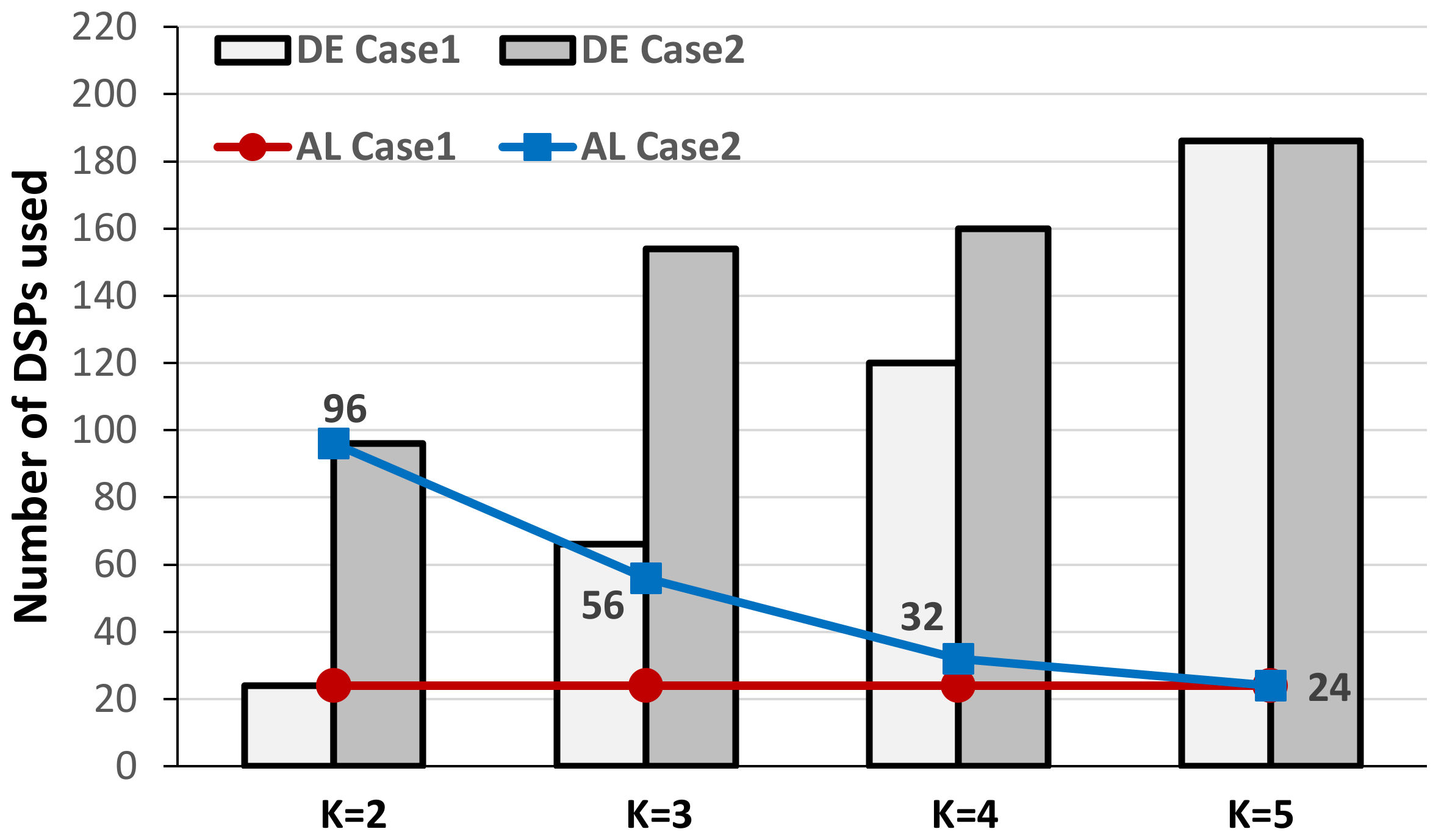
PM, and PN. Establishing which configuration is the most appropriate for a specific operating environment is crucial to use the available resources as more efficient as possible. To this aim, different design spaces can be explored by varying the above parameters. As an example, the design space exploration reported in
Figure 11 was carried out by considering the XC7Z020 device as the target, thus setting the maximum number of available DSPs to 220. The behavior of the proposed accelerator has been examined for various kernel sizes
K and parallelism levels
TM and
TN with
S = 2,
PM = 4 and
PN = 1. In this condition, two different scenarios were analyzed: in the first case (the Case1 in
Figure 11),
TM = 2 and
TN = 3 are maintained unchanged to establish the maximum supportable kernel size; conversely, in the second case (referred as the Case2) also
TN varies between 24 and 6, while
TM is set to 1. In the case 2, for each
K the maximum
TN has been considered (e.g., with
K = 2,
TN = 24).
Figure 11 plots the numbers of DSPs used in the two referred cases by the DE and the AL versus
K. As expected, in the first case the wider the kernel size, the higher the number of DSP slices required by the DE. On the contrary, the red line shows that the number of DSPs used to implement the fast adder trees within the AL module is maintained constant to 24, since it only depends on the parallelism and the stride. The above results show that in such a case, the maximum kernel size supportable with 220 DSPs is
K = 5. This is the solution above referenced in
Table 1 for both the SU and ES designs implemented within the XC7Z020 device.
Results collected for the second analyzed scenario prove that to comply with the amount of DSPs on-chip available, as the kernel size increases, the parallelism must decline. Obviously, as clearly shown by the blue line in
Figure 11, the lower the parallelism, the lower the number of DSPs used for accumulations. The possibility of having different design spaces to explore helps the designer in identifying the best configuration of the proposed DLPE for a certain specific operating condition.
Finally, referring to the XC7Z020 device, the execution time of the ES implementation here proposed has been compared to a pure software design run by the 666 MHz ARM-Cortex Processor on-chip available. When executing the most complex deconvolution layer involved in the selected DCGAN model [
21], the ES, which integrates the novel DLPE as the hardware accelerator, is more than 1000 times faster than the all-software implementation.


