2.2. Characterization Methods
The XPS analyses were performed by using an Omicron EA 125 electron spectrometer (Omicron NanoTechnology GmbH, Taunusstein, Germany) in the “Fixed Analyzer Transmission” mode; photoelectrons were excited by non-monochromatized MgKα (1253.6 eV) radiation. The energy scale of the electron spectrometer was calibrated according to the ISO 15472 standard. The estimated uncertainty of the binding energies obtained in this work is around ±0.2 eV. Samples were investigated in their “as received” state, without any cleaning in solvents. High-resolution spectra were obtained from the regions of interest using a “pass energy” of 30 eV, providing resolution around 1 eV. Spectra were processed with the CasaXPS package (Casa Software Ltd., v.2.3.12, Teignmouth, UK) [
29], while quantitative evaluation of the data was performed with the XPSMultiQuant package (M. Mohai, v.7.00, Budapest, Hungary) [
30], during which a homogeneous depth distribution was assumed for all components. As the line shape of the Mo 3d spin-orbit doublet suggested the almost exclusive presence of the Mo
6+ ionic state, the referencing of the binding energy scale was possible by setting the maximum of the Mo 3d
5/2 peak to 232.5 eV, which is the binding energy reported for Mo
6+ ions in MoO
3 [
31,
32]. This correction was confirmed by the resulting C 1s binding energy slightly below 285 eV.
The crystallinity of the layers was investigated by X-ray diffraction (RIGAKU SMARTLAB diffractometer, Tokyo, Japan) in Bragg–Brentano geometry using Cu K-α and K-β radiation. The crystallinity of the samples is defined by the ratio between the total sample intensity and the intensity of the crystalline phase peaks, namely,
The steps to obtain the crystallinity consisted of deduction of constant background, a rough linear fitting of amorphous phase, integration of different phases via Simpson method, and lastly calculating the crystallinity. In the case of crystalline layers, a clear, good quality reflection (i.e., without overlapping with other peaks) was selected and scanned with monochromatized K-α radiation in grazing angle. Afterward, by analyzing the X-ray line profile with the so-called restricted moments method developed by Groma et. al. [
33,
34], the average dislocation density and average grain size were determined. From the asymptotic behavior of
kth order restricted moments
of the measured
I(
q) X-ray intensity distribution, one may obtain
and second order and fourth order restricted moments, respectively. In the above equation,
is the diffraction distance, where
θ0 is the exact Bragg-angle and
λ is the wavelength of the applied X-ray radiation. One can clearly see that both the average dislocation density
and average grain size (
1/
d) appear in the second and fourth-order restricted moments, which means that one can determine these parameters by subtracting the appropriate background and fitting the restricted moments [
35].
To investigate the mechanical properties of MoO
3-bearing layers, a custom-made nano indenter was used [
36,
37]. The developed apparatus is suitable for the investigation of the nano deformation methods by its fast response speed and mountable acoustic emission (AE) sensor, besides the crucial mechanical properties. An AE signal could form during plastic events, such as crack formation and crack propagation, cooperative dislocation movements, and different types of phase transformations [
38]. The detection of AE is based on the elastic energy release due to the irreversible change in the specimen’s (micro)structure. Near the AE source, the released energy forms a stress pulse, which propagates through the material. The elastic stress wave component, which is perpendicular to the surface, is detected by piezoelectric transducers, which are coupled to the specimen’s surface mechanically [
39]. For the nanoindentation analyses, a diamond Berkovich-type indenter tip was used. The accuracy of the depth and load measurements were 1 nm and 1 µN, respectively, and the applied sampling rate was 200 Hz. In this indentation measurement, there was no applied load or strain control to avoid the artificial effects of the electrical feedback. The spring attached platen velocity was set to a constant value to carry out the tip penetration, which was proportionate to the average indentation rate. In the case of AE measurements, the sampling rate of the data streaming was 2 MHz (adjusted to the known main signal frequency of 50–500 kHz). The signal detection threshold set to 0.01 mV was remarkably over the noise level.
Morphological and microstructural characterizations of the thin layers were carried out with focused ion beam/scanning electron microscopy (FIB-SEM) system using FEI Quanta 3D dual beam scanning electron microscope. The as-prepared, heat treated at 200 °C and 300 °C layers were analyzed pre and post-nanoindentation in order to visually inspect the indentation effect on the layers and their patterns.
The assembled battery cells were cycled between 1 and 3.5 V under galvanostatic conditions using a Biologic VMP-300 electrochemical workstation. The initial 10 cycles were performed at a rate of C/2, followed by long-term cycling at 10C for an additional 500 full cycles.
2.3. Results and Discussion
(1) Chemical and crystallographic characterizations
Chemical composition including the Mo:O atomic ratio of the as-sputtered and the annealed thin films were characterized by XPS. Results of the quantitative analysis are presented in
Table 1. All examined surfaces contain a relatively high amount of carbon. As even a minimal in situ ion bombardment very significantly decreased the carbon content, it was assigned to surface hydrocarbon contamination adsorbed from ambient air. Indeed, the binding energy of the main C 1s peak around 284.8 eV is characteristic of hydrocarbon contamination.
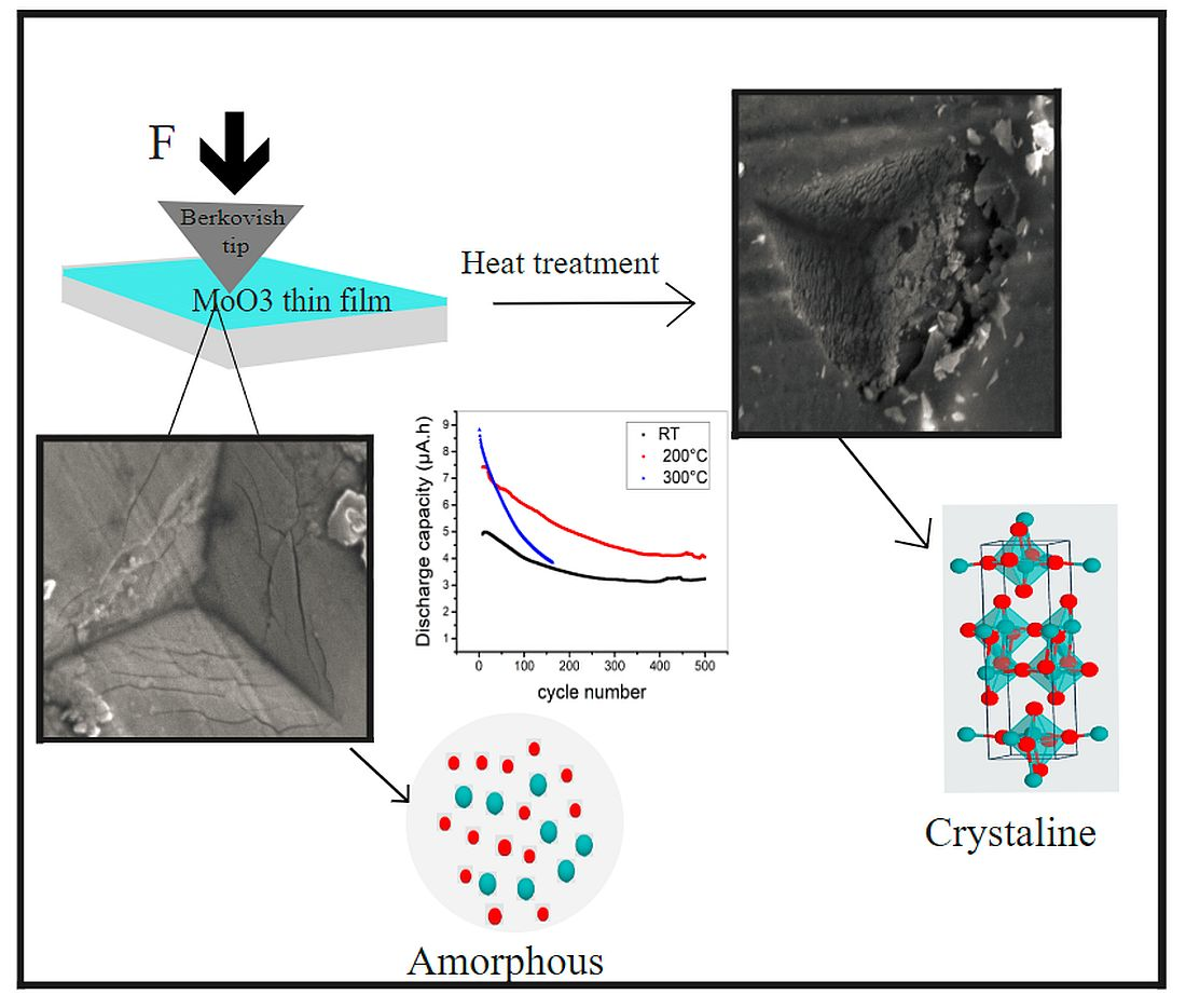
Figure 1 shows the detailed Mo 3d spectra of the three samples. Most of the Mo 3d signals are assigned to the 3d
5/2−
3/2 spin-orbit doublet of the Mo
6+ ions (3d
5/2 component at 232.5 eV binding energy). The width of the Mo
6+ peaks clearly decreased with increasing annealing temperature (full width at half maximum of the Mo
6+ 3d
5/2 peak was 1.54 eV, 1.44 eV, and 1.23 eV for the untreated, 200° C, and 300 °C annealed samples, respectively). This suggests a more uniform, ordered local environment for the Mo ions in films annealed at higher temperatures. At the same time, a slight asymmetry at the low-binding energy side of the main peaks indicated the presence of another chemical state, which was slightly more pronounced in the 300 °C sample. It was modeled by a second spin-orbit doublet, which accounted for roughly 4–5% of the total Mo signal in the untreated and the 200 °C annealed sample and 7% in the 300 °C sample. According to its 3d
5/2 binding energy around 231 eV, it was assigned to Mo
5+ ions [
31].
The O 1s spectra of the samples were rather similar; they were dominated by a peak at 530.4–530.6 eV arising from lattice oxygen in Mo-oxide, while a weak component at its high binding energy side contained contributions from surface hydroxyl groups as well as from carbon-bound oxygen atoms belonging to the carbonaceous contamination. All surfaces were somewhat oxygen-deficient. The Mo:O ratio in the untreated sample was 1:2.60, which hardly changed in the 200 °C-treated sample but decreased below 1:2.50 in the 300 °C sample. The results of the XPS investigations suggest that our cathode material consists of MoO3 with a Mo:O ratio close to 1:3; although, some variation in the microstructure is expected as a consequence of the annealing.
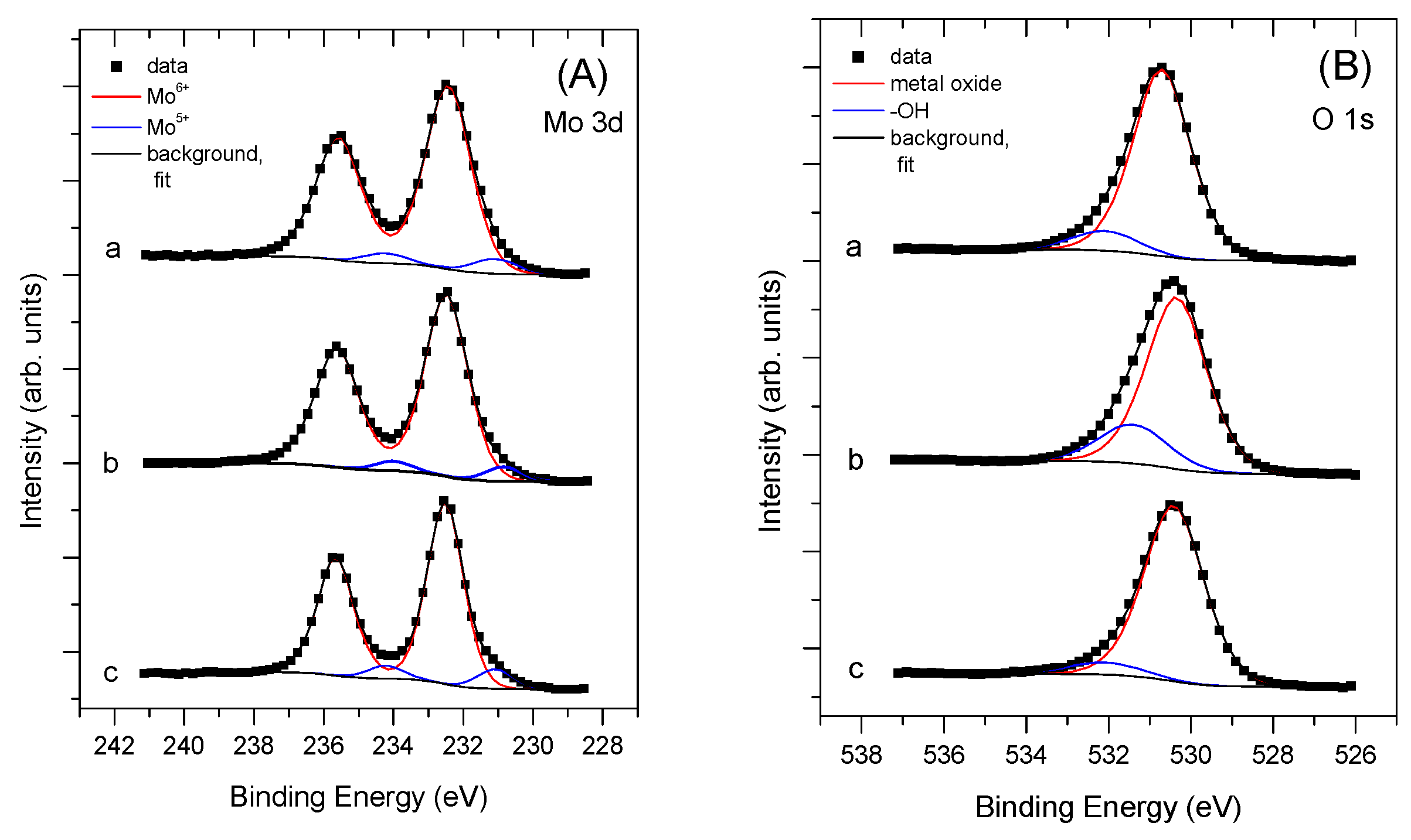
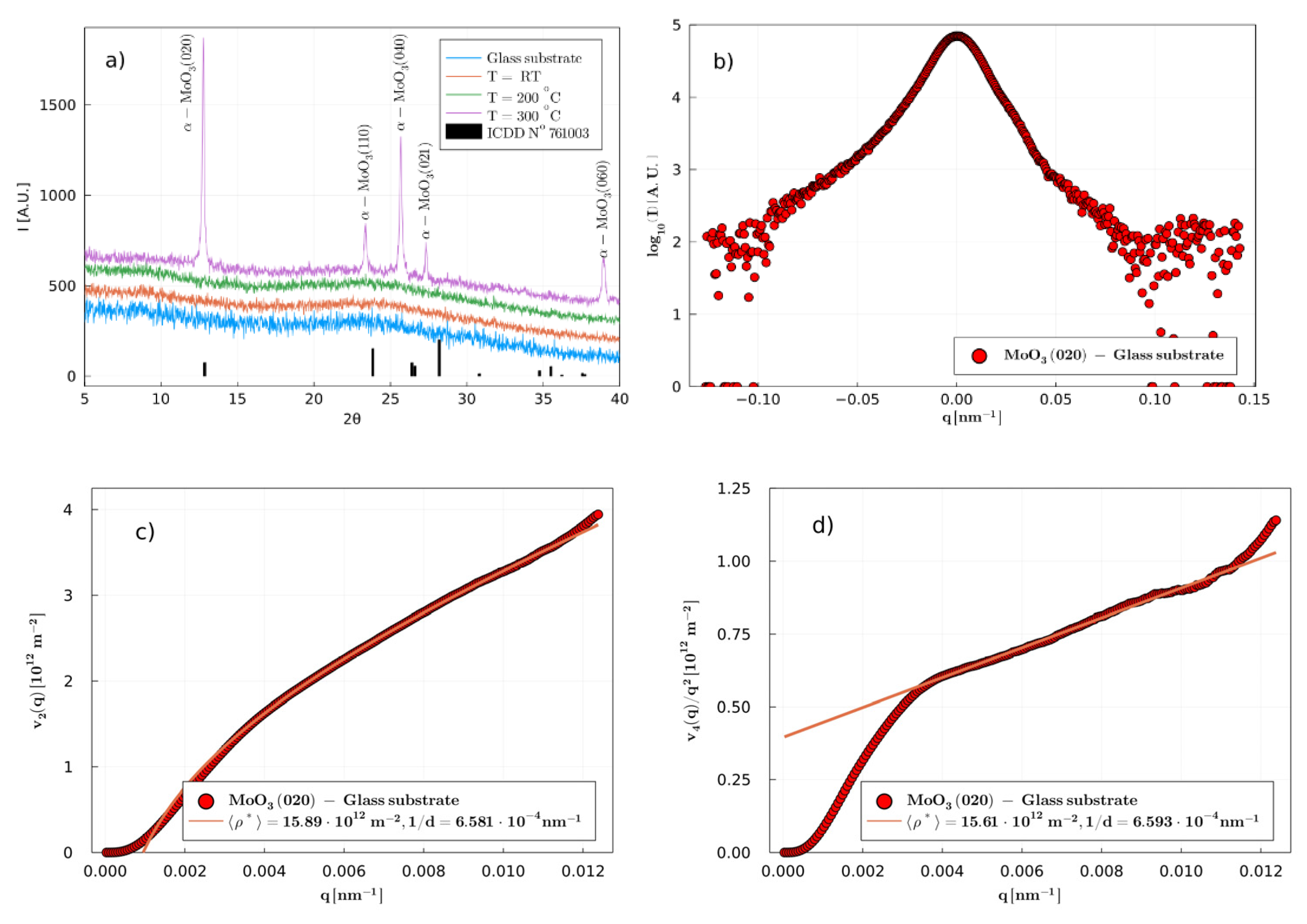
To reveal the crystallographic features of the as-sputtered and the annealed MoO
3 thin films, XRD measurements were carried out. The diffractogram measured in Bragg–Brentano geometry of the as-sputtered MoO
3 thin film does not present any peaks, meaning the layer is completely amorphous (
cf. Figure 2a). When heat treated at 200 °C, the layer still presents its amorphous features, while crystallization only took place when the layers were heated to 300 °C. The diffractograms of the thin films grown on aluminum substrate show the orthorhombic α phase of MoO
3 referred to with a delta symbol; however, impurities (namely, multiple AlO
x phases) referred to with a star symbol are also observed. The appearance of the AlO
x phases can be attributed to the conventional heat treatment procedure.
As was stated earlier, the calculation of the grade of the crystallinity of the thin layers before and after annealing was made in an approximate but simple manner, which is useful for the analysis of Bragg–Brentano data with multiple peaks. The fluctuating background (
BG) was fitted via a two-point linear fitting, while the peak intervals were left out, via linear bridging (see
Figure 2). Afterward, the amorphous background was subtracted from the whole diffractogram, obtaining the diffraction peaks corresponding to only the crystalline MoO
3-α phase. In the next step, the original diffractogram and the crystalline phases were integrated via the Simpson method. The samples annealed below 300 °C had a rather amorphous character, they were 0% crystalline; however, those that were heated to 300 °C exhibited 5.4% crystallinity on the aluminum substrate. The low crystalline character in the case of the samples processed and deposited onto the aluminum substrate could be explained by the appearance of AlO
x phase impurities, which could have had a pinning effect on the growth of MoO
3 grains.
The annealed MoO
3 thin layers deposited onto glass substrate showed a higher crystallinity grade especially for the 300 °C heat treated sample (see
Figure 3a). It was calculated to 9.6% (on glass), in contrast to the 5.4% calculated crystallinity for the aluminum substrate-processed supported samples.
The average dislocation density and grain size of the MoO3 films on glass substrate were estimated by the momentum method. In fact, inner stresses of the thin aluminum foil substrate were released via physical distortion such as bending and deflection during the heat treatment, resulting in the cracking of the MoO
3 thin film. Accordingly, the momentum method was applied for the crystalline sample prepared on the glass substrate. In fact, the momentum method was not applied in the case of the thin films prepared on aluminum substrate. The reason for this was due to the heat treatment of the thin films; the inner stresses of the thin aluminum foil substrate were released via physical distortion, namely, bending and deflection, so the thin film cracked on the surface of those. Since the momentum method is sensitive for such length scale-inducing effects and would not even correctly predict the average dislocation density, it cannot be used for the films on the aluminum substrate. However, in the case of glass substrate samples, coherent results were obtained regarding the parameters from second and fourth-order restricted moments (
Figure 3c, respectively
Figure 3d.) The obtained average dislocation density
and average dislocation cell size d ≈ 1.4 are expected results for a partially recrystallized, fairly large, grained sample. In this case, we can assume that, truly, the average dislocation cell size is equivalent to the average grain size, because the obtained value is in the range of microns. However, this is not always true, because for extremely large-grained polycrystals (10–100 µm), the characteristic length of the dislocation structure will always be smaller than the size of the crystallites. Since the thin film has a thickness of 10–100 nm, the average grain size is obtained based on surface data, which means that the grains have a large anisotropic extent on the x-y plane in comparison to the z direction.
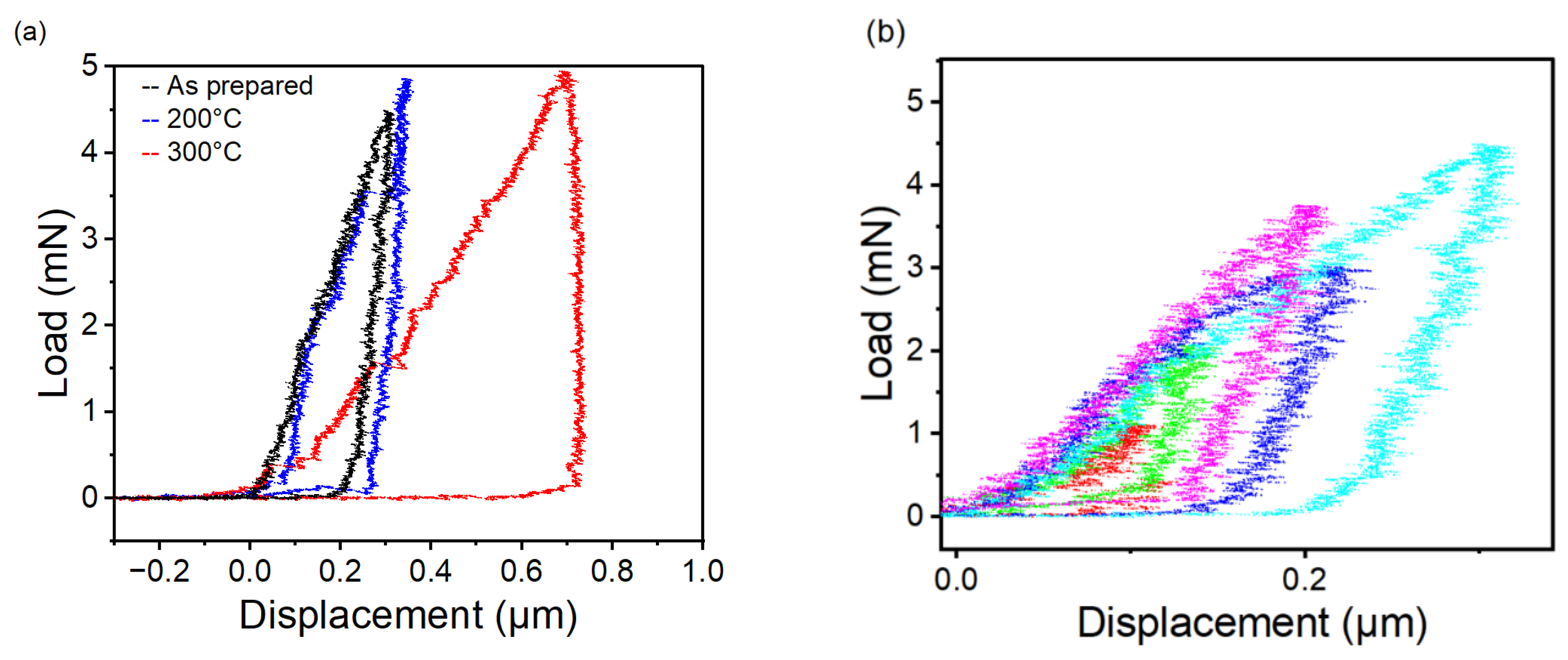
Mechanical hardness tests were performed on the thin layers sputtered on the aluminum substrate, which is the selected substrate that will serve later as the current collector for the MoO
3 cathodes in the thin-film Li-ion batteries. Six indentations were performed on each sample with different maximum applied forces up to F = 40 mN.
Figure 4a presents ones of the load vs. displacement curves for the three layers: as prepared, heat treated at 200 °C and 300 °C.
At first glance, it can be noted that the lowest maximum displacement recorded with the F = 5 mN load among the three different samples was found for the amorphous layer with penetration of 0.22 µm, followed by the layers heat treated at 200 °C and the 300 °C, with 0.3, and 0.7 µm respectively, which reflects the hardness conditions. Based on these three curves, we can conclude that the as-prepared and the 200 °C annealed samples have similar mechanical properties, unlike the 300 °C annealed one. As the indenter’s tip penetrates the specimen, the loading curve raises. At some point, the maximum load Pmax is reached, which is then followed by the unloading.
The black and blue curves that belong to the as-prepared and 200 °C heat treated at 200 °C layers show the usual behavior of amorphous layers [
40], which shows that the deformation was mostly determined by the amorphous phase even in the sample heat treated at 200 °C. In the case of the 300 °C-treated and thereby more crystallized layer (red curve), there were two main differences compared with the other samples. First, under a given load value, the indenter’s tip can penetrate deeper into the sample, which characterizes softer materials (
Figure 5). Secondly, during the unloading part, the displacement did not decrease. This means that during the loading part, elastic energies do not accumulate and are stored in the material, only plastic deformation has occurred.
During the loading phase of the as-prepared, amorphous layer, the load curve is continuous; there are no sudden jumps. This smooth curve behavior is linked to the deformation mechanism. In these cases, the deformation was homogeneous in space and time, and shows the elasticity storing capability of the amorphous phase. This can be also confirmed from the rest of the load vs. displacement curves of the as-prepared layer (
Figure 4b) in five of the indentation curves present the same pattern.
The 300 °C heat-treated layer showed momentary jumps in the load vs. displacement graph. During these jumps a sudden plastic event occurred, where the load value remained close to constant, but the displacement had a sudden increase. These sudden deformation events could have more sources, such as the avalanche-like dislocation gliding and creeping, crack formation, and layer separation from its substrate. The possibility of these various and complex superposition-like deformation processes could serve as an explanation for the lack of the crystalline phase’s elasticity.
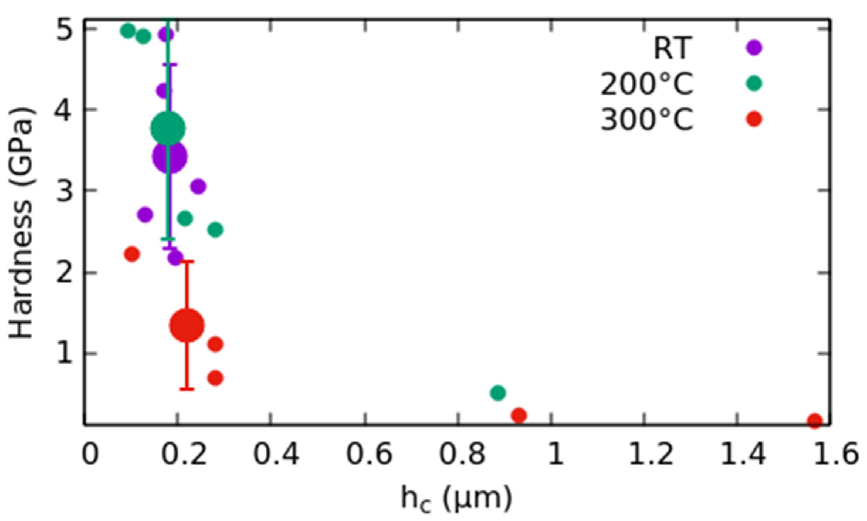
The hardness H (GPa) depends on the maximum force P
max (mN) applied to the thin layers and the indentation depth (h
c (µm)) corresponding to the contact surface. Its value can be calculated from the following equation. The h
c can be determined by the point of intersection of the linear fitting to the first part of the unloading with the zero load the linear line x in the line projected to the initial values of the load curve [
41].
Further investigations on the hardness (
Figure 5) revealed that in the case of higher penetration than 0.4 µm, the hardnesses were lower (around 300 MPa); these results were coming from the aluminum substrate and not the layer, as the penetration exceeded the layer thickness, which is in a good agreement with the expectation [
42]. In order to have more accurate results of the hardness, all penetrations below 0.4 μm were averaged and presented with the larger circles.
Regarding the hardness of the MoO3-bearing layers, there is a slight difference between the amorphous and the heat-treated sample at 200 °C. The thin-film sample heat treated at 300 °C is much softer than the previous ones due to its different deformation properties.
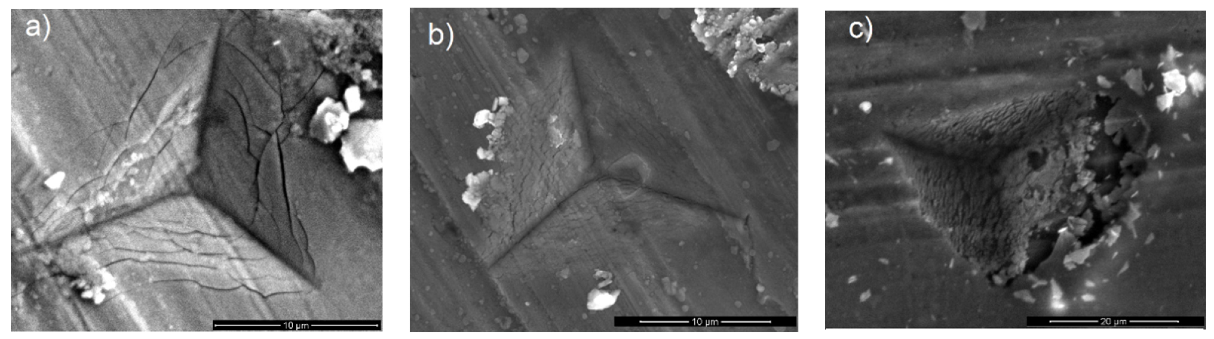
The indented layers were examined using scanning electron microscopy (SEM). Due to the semiconductive nature of MoO
3, the samples were carbon coated to a thickness of 7 nm as measured with a quartz crystal thickness gauge. The brittleness and the adhesion of the layers could be represented by the number of cracks. According to
Figure 6a, the most elastic as-prepared layer shows the least number of cracks (as expected), followed by the heat-treated layer at 200 °C, as presented in
Figure 6b. The number of cracks is the highest for the 300 °C layer (presented in cf.
Figure 6c). In this figure, there is visible proof of the peeling of the layer from the substrate, which is in good agreement with the above section regarding the elastic conditions. This different peeling behavior was also expected. When a huge strain was applied on the substrate (cased by 40 mN load), the more elastic layer can follow better the deformation of the substrate and stay in contact.
Acoustic emission measurements were performed in parallel with the nanoindentation studies. Crack formation and its sudden propagation, or the cooperative motion of the dislocations in the layers during indentation can form a significant acoustic signal [
39], while the slow deformation processes, such as the grain boundary sliding or the atomic rearrangement near local stress zones and free volumes (which characterize a common deformation process in amorphous materials [
43]), produce no detectable acoustic signals.
This was in perfect agreement with the results obtained since the as-prepared layer did not produce any signals, while most of the acoustic emission signals were obtained from the samples heat treated at 200 °C and 300 °C. Altogether, four acoustic signals were detected during the six indentation runs from the samples heat treated at 200 °C, and four acoustic signals in case of 300 °C. The heat-treated samples are crystallized to some degree, but we cannot connect the AE signals clearly to the crystalline form, since there were no differences between the AE signals regarding the degree of crystallinity. Acoustic signals may be generated from the cracks, and in the case of the 300 °C heat-treated 300 °C sample, the more cracks cannot produce more AE signals, because of the poorer adhesion of the layer.
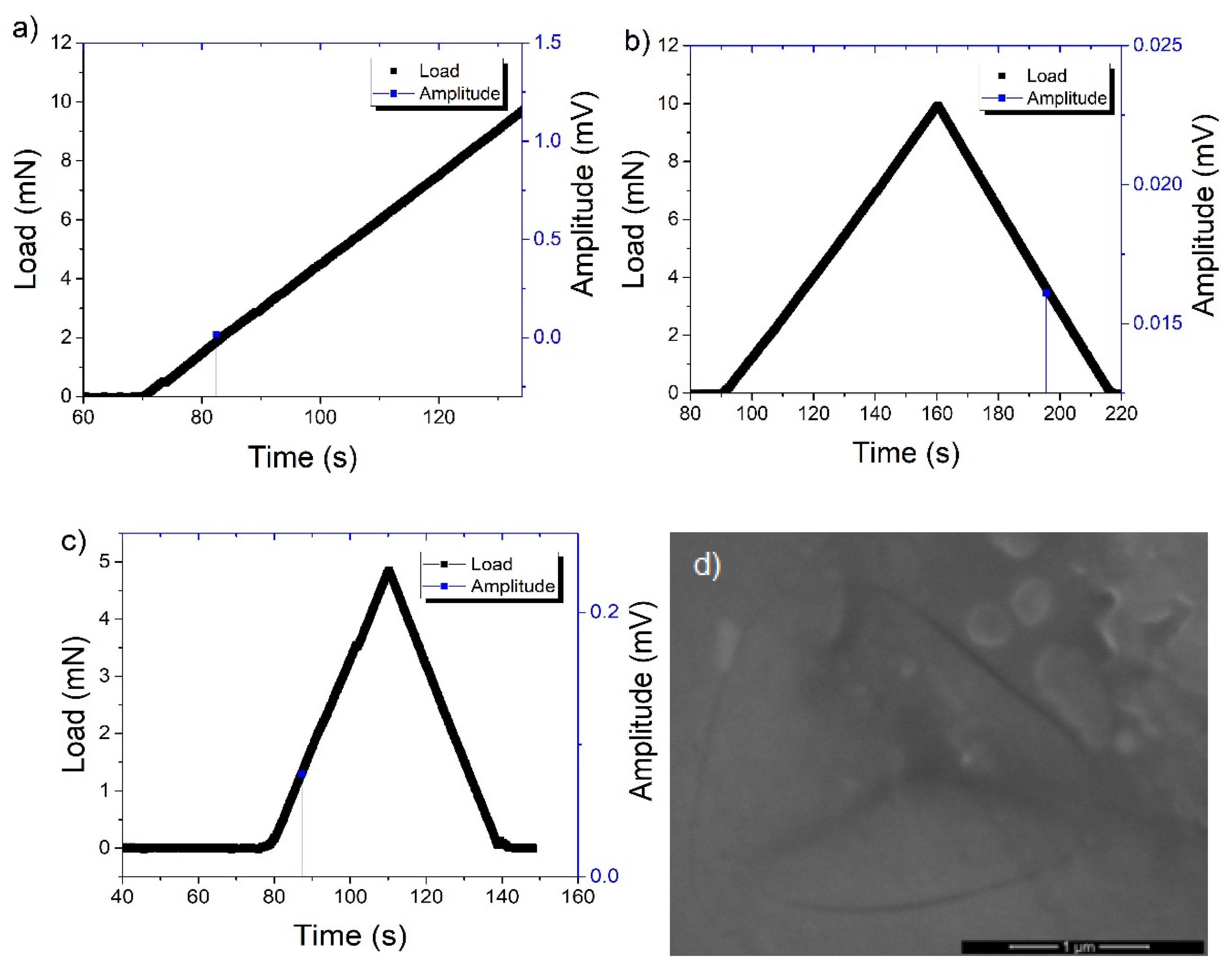
The load and the amplitude of the acoustic emission signal are plotted as a function of the time during the indentation using a 10 mN maximum load (
Figure 7). The detected AE signals were mostly in the loading part. In the fully crystalline most crystallized cases, there were AE signals during the unloading part (
Figure 7b). This type of event was not unexpected in a rigid, totally plastic material, because it is shown in
Figure 4a that during the unloading part, the tip’s penetration could increase, so plastic deformation occurred. The lack of the AE events during the unloading part of the amorphous layers also shows that the leading deformation mechanism belongs to the amorphous parts. However, the existing AE signals of the 200 °C-treated layer show that there is some contribution of the substrate to the deformation mechanism.
An interesting feature of the acoustic emission is that it can produce a signal after a crack as mentioned above.
Figure 7c shows the acoustic emission signal during the loading phase; furthermore, the SEM image of the crack produced on the surface of the MoO
3 layer heat treated at 200 °C is shown in
Figure 7d. It can be assumed that this crack formed at around F = 1.3 mN before the peeling out of the layer, since, during the crack formation, there was a good mechanical connection between the layer and the substrate, which makes it possible for the AE signal to propagate through the substrate to the detector from the crack in the layer.
In summary, the as-prepared MoO3 layer has been proved to have the highest hardness and elasticity from the load–displacement curves. This higher elasticity was also proven by the fact that the as-prepared layer did not produce any acoustic emission signals. This means that the main deformation mechanisms of the as-prepared layers are the acoustically silent atomic rearrangements. In these cases, the separation of the layer from the substrate is assumed to be the reason for the crack development or it occurred before the crack formation. The heat-treated layers, however, showed some jumps in the load–displacement curve; this can tell us about certain deformations/crack formation in the layer during the indentation, which is supported by the acoustic emission signals. It can be concluded that the main deformation mechanism was the cracking of the layer, which confirms their brittleness. From the SEM images of the indentation, it can be deduced that the heat treatment resulted in poor adhesion between the layer and the substrate, which could be due to the phase change from amorphous to crystalline. The use of the nanoindentation, acoustic emissions, and SEM images can tell us a lot about these properties of supported thin films.
To conclude this section, X-ray diffraction confirmed the amorphous nature of the as-sputtered MoO
3 thin films. According to surface mechanical studies, these films are adherent, hard, and elastic. As suggested by the XPS measurements, annealing of the films at 300 °C in air resulted in partial crystallization producing large grains elongated on the plane of the film. These films were rigid and brittle, with a tendency for peeling under mechanical stress. However, a significant amount of Mo-oxide remained in a disordered state even after this heat treatment. It can be assumed that the relatively large oxygen deficiency of the 300 °C annealed films, along with the increased Mo
5+ content revealed by XPS, is related to the presence of this disordered fraction. Nevertheless, our results are consistent with the literature data suggesting the transition between amorphous and crystalline MoO
3 at around 300 °C [
44,
45]. Mechanical properties of the films annealed at 200 °C in air still show the prevalence of the amorphous oxide but are in some sense intermediate between those of the as-prepared and the 300 °C annealed systems. Although long-range ordered crystalline domains were not detected in these samples by XRD, their mechanical behavior, as well as slight changes in the Mo 3d XPS spectrum, is in line with the increasing local ordering.
(2) Electrochemical characterizations
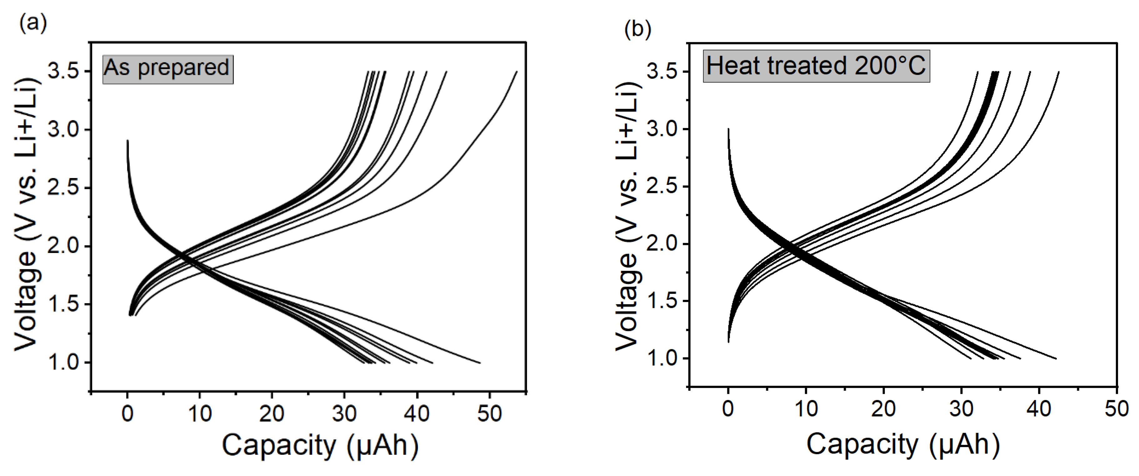
The electrochemical cycling behaviors at I = 25.25 μA charge/discharge currents of the battery cells assembled using the as-sputtered, 200 °C and 300 °C heat-treated samples are depicted in
Figure 8. The charge–discharge curve consists of smooth S-shape profiles at any cycle without having a flat plateau average voltage of about 1.9 V. As shown in
Figure 8a,b for the as-sputtered and the 200 °C heat-treated samples, a rather high initial irreversible capacity was observed, which was smaller in the case of the sample heat treated at 300 °C (
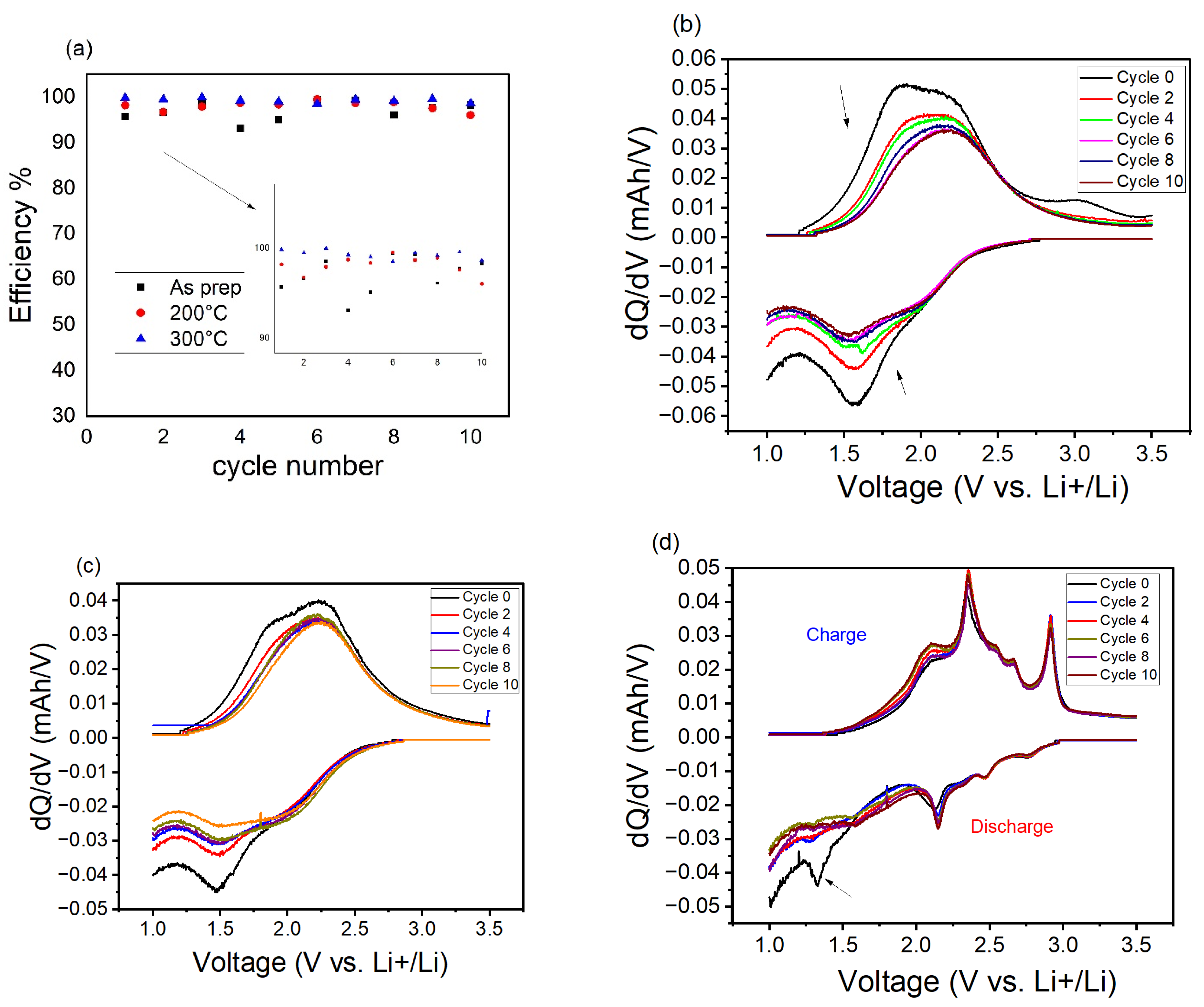
cf. Figure 8c). In fact, the as-sputtered cell showed the highest initial capacity of around 50 μAh compared to 44 μAh for 200 °C and 35 μAh for the electrode heat treated at 300 °C. On the other hand, the best coulombic efficiency (
Figure 9a) was for the 300 °C heat-treated layer at 300 °C followed by the 200 °C heat-treated layer at 200 °C and, finally, the as-prepared layer.
In terms of coulombic efficiency (
Figure 9a), the heat-treated layer at 300 °C showed superiority compared to the layer heat treated at 200 °C and the as-prepared amorphous layer.
Differential capacity curves of MoO
3 electrodes heat treated at different temperatures are shown in
Figure 9b–d. In
Figure 9b, the charge branches (positive current values) of the cycling data show a broadened character without sharp signal peaks, which may be attributed to the amorphous nature of the applied cathode material and the broad energy distribution of the reaction sites in the electrode active material [
19].
Compared to the as-prepared electrode layer, the electrode layer treated at 200 °C shows similar electrochemical behaviors, which can be explained by the similar, predominantly amorphous structural features discussed above. The as-prepared and the 200 °C-treated electrode layers are rather amorphous and therefore similar electrochemical performance is expected. In fact, the electrode layer treated at 300 °C shows remarkably different electrochemical behavior than the previous ones. Sharper and more intense peaks compared to the amorphous and the 200 °C layer can be observed on its incremental capacity curves (charge and discharge, cf.
Figure 9c,d), and this could be correlated to the crystal phase structure of the electrode, as previously confirmed with the XRD analyses, i.e., the heat treatment at 300 °C led to the partial crystallization of the MoO
3 layer. The 300 °C heat-treated MoO
3 layer presented in the differential capacity curve (
Figure 9d) exhibits two strong peaks at 2.4 V and 3 V, observed during the charging process, and two reversible signals at 2.2 V and 2.6V during discharge, while a peak at 1.4V arises due to an irreversible electrochemical process; its intensity diminishes with the consecutive cycles.
The multiple peaks during charge/discharge for the layer heat treated at 300 °C can be explained by its partial crystallization; in other words, Li
+ was inserted into both the crystalline and amorphous sites. Since orthorhombic MoO
3 possesses a layered structure, the peaks at 3V/2.2V, which are in perfect agreement with the literature [
46,
47], can be attributed to the insertion/extraction of Li
+ ions in the interlayers of the crystalline MoO
3, while the rest of the peaks are assumed to be part of the insertion/extraction of Li
+ ions in the amorphous regions of the thin layer.
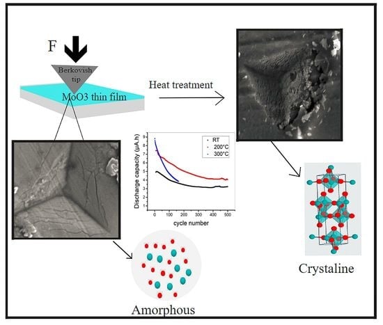
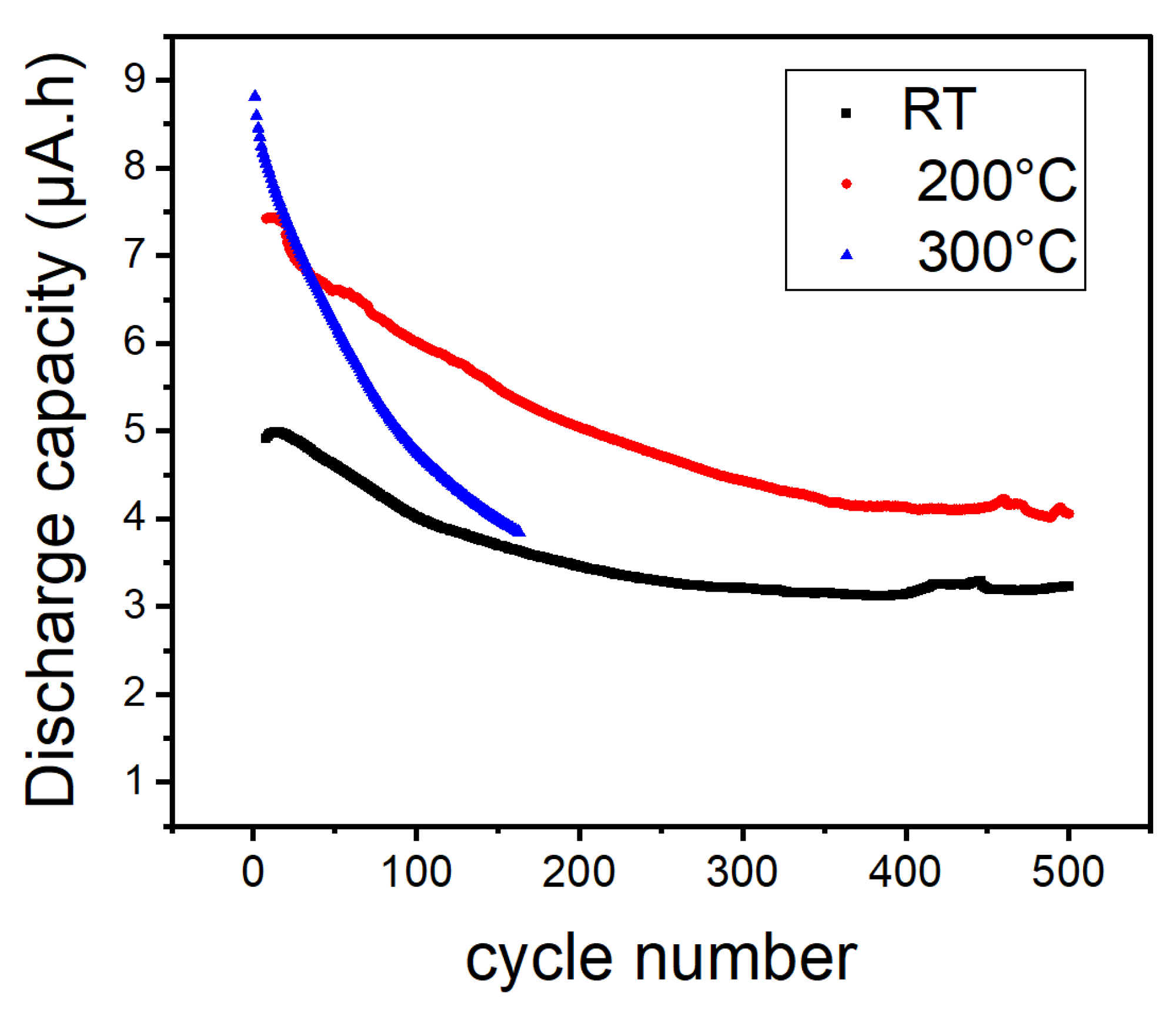
The as-prepared layer showed good stability throughout the 500 full cycles compared to the heat-treated layer at 200 °C and more specifically to the layer treated at 300 °C, which experienced a significant capacity loss and eventually a cell failure after reaching 160 cycles (see
Figure 10). This cell failure was expected, and it is in accordance with the nanoindentation and SEM results that indicate the more brittle structure of the crystalline layer, which is more prone to the electrochemically induced internal stresses and the concomitant delamination and detachment from the metallic current collector, which is assumed based on the nanoindentation and hardness analysis mentioned above. Amorphous MoO
3 shows increased cycling stability, although with less defined electrochemical features, which is in accordance with previous publications [
47].


 ,
, 


