Article

Electro-Thermal Modeling and Simulation of a Battery-Integrated PECIN Multilevel Inverter Using a Switching Model Approach

by
Sascha Speer
*,
Christoph Terbrack
and
Christian Endisch
Research Group Electromobility and Learning Systems, Institute of Innovative Mobility, Technische Hochschule Ingolstadt, D-85049 Ingolstadt, Germany
*
Author to whom correspondence should be addressed.
Batteries 2026, 12(5), 181; https://doi.org/10.3390/batteries12050181
Submission received: 31 March 2026 / Revised: 11 May 2026 / Accepted: 12 May 2026 / Published: 20 May 2026

Abstract

Cascaded multilevel inverters constitute a promising system concept for battery electric powertrains due to their high efficiency, low harmonic distortion, and advanced battery management capabilities. This study presents a novel electro-thermal simulation framework for the symmetrical Parallel Enhanced Commutation Integrated Nested (PECIN) multilevel inverter. The proposed model employs a control-oriented approach that enables the development and evaluation of advanced inverter and battery control algorithms, which exploit the extensive series-parallel reconfiguration capabilities of the PECIN topology. The framework is based on electrical and thermal equivalent circuit models to capture physical behavior and cross-domain interactions. Electrical network analysis employs algorithms that iterate over each phase-arm network, replacing high-dimensional matrix inversions and thereby enhancing computational efficiency. The overall model is readily adaptable to various system configurations, including different AC and DC charging modes, and scalable with respect to the number of submodules and phases. Simulation results for a 31-level multilevel inverter in a three-phase AC charging configuration demonstrate the model’s operational capabilities. Execution time analysis shows that the current distribution calculation is the key contributor to computational effort as the number of submodules increases, resulting in a quadratic growth of the overall computational time.

Graphical Abstract

1. Introduction

As the global demand for greener solutions intensifies, battery electric vehicles (BEVs) have become a vital part of the strategy to lower carbon emissions and address climate change [1]. The central component of state-of-the-art BEVs is the electric powertrain, typically comprising a traction battery with its associated battery management system, a two-level inverter, an electrical machine, and an integrated onboard charger. While this system configuration provides a robust and well-established foundation, the rigid interconnection of individual battery cells—combined with intrinsic variations in capacity and internal impedance arising from manufacturing tolerances and operational conditions [2]—limits the utilization of the battery system’s total energy content. Moreover, the overall performance of the battery pack is constrained by the weakest cell, which determines the permissible operating limits of the entire system [3,4]. The variable battery voltage further reduces the efficiency of the two-level inverter, as it prevents consistent operation at the optimal point [5].
The battery-integrated cascaded multilevel inverter (MLI) represents a system-level approach to overcoming these technological limitations and further enhancing BEV performance. The fundamental unit in a cascaded MLI is the submodule (SM), which occurs in a repetitive arrangement. Each SM comprises one or multiple battery cells along with a characteristic switching topology. The discrete voltage levels of the MLI are defined by the voltages of the constituent battery cells. By combining multiple voltage levels, the MLI can directly generate AC output voltages with inherently low harmonic distortion [6]. Compared to conventional two-level inverters, cascaded MLIs achieve a substantial reduction in switching losses and voltage stress across individual switches [7,8]. This contributes to the superior efficiency of cascaded MLIs [9]. In BEV applications, the cascaded MLI also eliminates the need for an onboard charger and reduces filtering requirements [9,10].
The literature discusses various switching topologies within the SMs to implement cascaded MLIs [11]. These range from topologies with comparatively few switching elements per SM, allowing only serial reconfiguration, to highly complex switching topologies with additional parallel reconfiguration. The Parallel Enhanced Commutation Integrated Nested (PECIN) MLI represents an attractive topology, offering both series and parallel reconfiguration capabilities. The parallel reconfiguration reduces the effective resistance of the PECIN MLI in operation, enabling it to achieve efficiency comparable to that of leading topologies [12]. An operating strategy that integrates battery management with inverter functionality, while accounting for electrical and thermal interactions, is crucial for fully exploiting the potential of the PECIN MLI. The development of such a strategy constitutes a higly complex task, as it involves a large number of constraints and dependencies [13].
The design and optimization of operating strategies require sophisticated simulation models that capture the electrical and thermal dynamics of cascaded MLIs. The computational efficiency of these models is essential for analyzing system behavior within acceptable execution times of up to a few hours. However, the efficient modeling and simulation of large-scale cascaded MLIs often pose significant challenges, as several factors contribute to prolonged execution times [14,15,16,17]. A key factor is the large number of semiconductor switching elements and passive components distributed across numerous SMs [15,18,19,20]. As the number of SMs increases, the dimensions of the vectors and matrices required to describe the system dynamics increase proportionally. Solving the matrix-vector equations typically requires a complex matrix inversion, resulting in a cubic increase in computation time. Matrix inversion may be performed at each time step or whenever the switching state changes [18]. The accurate representation of high-frequency switching operations further necessitates a small time step size. Typical step sizes are in the range of several microseconds, which is another significant contributor to the increased computational effort [19,20]. For cascaded MLIs with pure serial reconfiguration capability, the SMs in each phase arm are electrically coupled only through the respective phase currents. In contrast, for cascaded MLIs with parallel reconfiguration, the current distribution between the SMs must additionally be accounted for. The additional calculations further increase the overall computational burden, as indicated in [21].
The application of cascaded MLIs in BEVs is a relatively recent research topic, whereas the underlying technology has a well-established history in high-voltage direct-current (HVDC) applications. Studies in this field have proposed efficient modeling methods for cascaded MLIs with series-only reconfiguration, with a primary focus on the modular multilevel converter employing half-bridge SMs [14,16,18,19]. Due to its favorable trade-off between accuracy and computational effort, detailed equivalent-circuit modeling has gained widespread acceptance. Within this approach, the converter switching dynamic is approximated by a linear equivalent circuit with time-dependent resistive elements representing the switching elements. This type of modeling retrains the internal electrical states of the individual SMs and offers the significant advantage of transforming the directly series-connected SMs in each phase arm into a Thevenin or Norton equivalent. This transformation markedly reduces the number of nodes and meshes in the electrical network, thereby shrinking the overall system’s matrix dimension by several orders of magnitude. This modeling approach is mathematically feasible without any loss of accuracy and is also employed in this study. The overall system dynamics of the cascaded MLI is determined in [16,18] using the nodal admittance matrix and in [14] using node potential analysis. Alternatively, mesh flow analysis can be employed, as in this study.
Existing studies on the modeling and simulation of cascaded MLIs [14,15,18,19,20,22,23] focus on a topology with only serial reconfiguration, whereas the computationally efficient modeling of cascaded MLIs with parallel reconfiguration has not been thoroughly addressed in prior research.
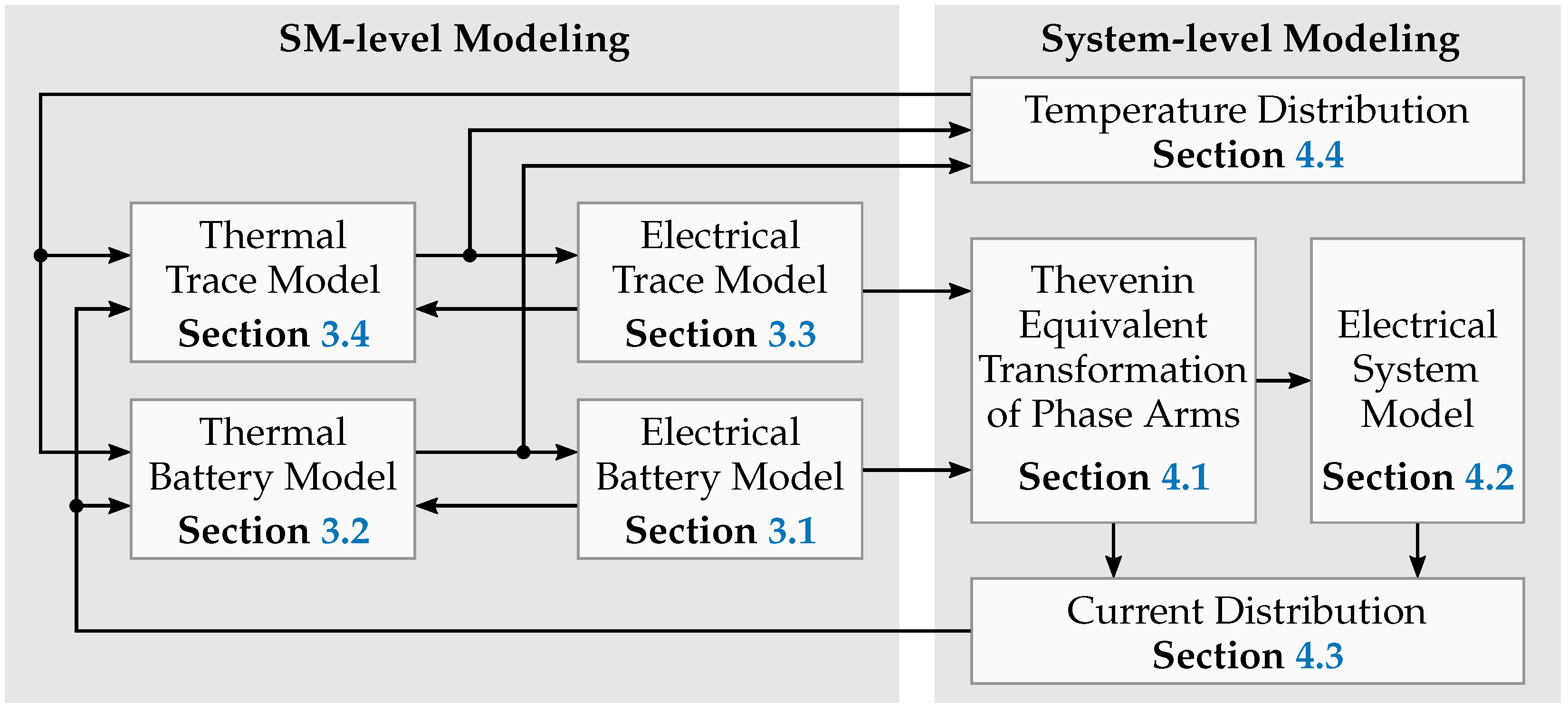
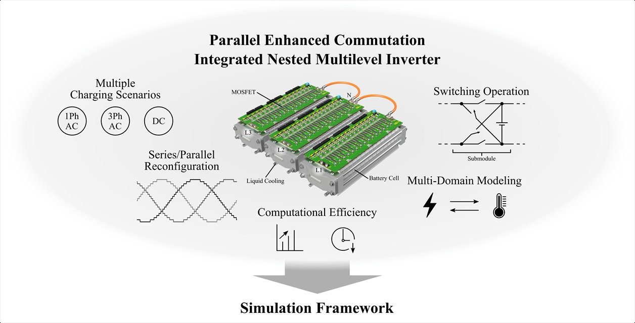
This study presents for the first time a comprehensive electro-thermal simulation model of a symmetrical PECIN MLI, enabling the development and evaluation of inverter performance under a range of operating conditions. A detailed switching modeling approach is employed to provide in-depth insight into inverter control. The model adopts a single-cell architecture, which allows for optimal utilization of each battery cell and offers maximum flexibility in control. The simulation framework integrates multiple submodels to capture both electrical and thermal system dynamics, facilitating a deeper understanding of PECIN MLI operation. This knowledge forms the basis for the design of multi-objective operating strategies. Figure 1 illustrates the structure of the simulation framework and highlights the Sections covering the individual model components. The remainder of the paper is structured as follows. Section 2 introduces the PECIN topology, its functional range, and the relevant modeling considerations. The following Section 3 introduces equivalent circuit models for describing the electrical and thermal behavior of the battery cells and switching paths at the SM-level. It also outlines the switching modeling approach used in this study. Section 4 provides a detailed description of efficient algorithms for system-level electrical analysis of PECIN MLIs, along with a thermal model capturing coupling within and between SMs. In Section 5, simulation results for a representative three-phase charging operation are presented to demonstrate the model’s capabilities, followed by an evaluation of its computational effort. Finally, Section 6 concludes with a summary and outlook.

2. Overview of the PECIN Topology

The PECIN topology investigated in this study was presented by Gupta and Jain [24] and Terbrack et al. [12]. Compared with other existing MLI topologies, this topology is characterized by a reduced number of switches per SM for the available functional range. Individual SMs can be bypassed or connected in a series or parallel configuration with other SMs. Moreover, each SM provides polarity reversal, allowing positive and negative voltage contributions to the overall phase voltage.
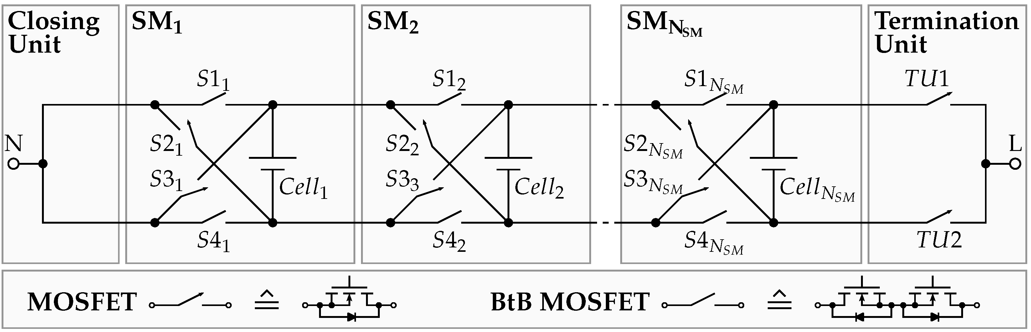
Four switching elements, S 1 to S 4 , per SM are implemented to provide these functionalities within the PECIN topology. The cascaded SMs represent an electrical quadripole. An additional circuit at both ends of a phase arm is required to establish a two-pole with N and L terminals. These terminals connect to an external load or supply. For the SMNSM that provides direct access to the cell terminals, a Termination Unit consisting of two additional switches, T U 1 and T U 2 , is required. This ensures that only one cell terminal is connected to the L terminal at a time. The two terminals of SM1, which provide access to its switching elements, can be electrically connected together within a Closing Unit.
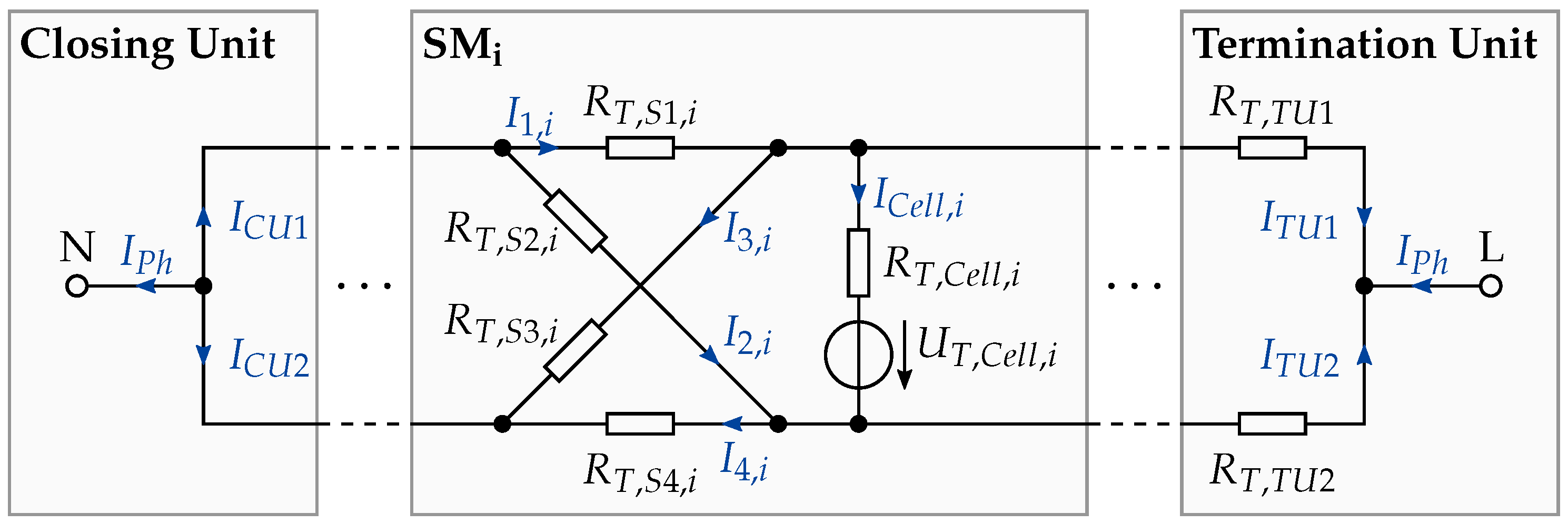
The switching network of a symmetrical PECIN MLI phase arm, shown in Figure 2, consists of N S M SMs, a Closing Unit, and a Termination Unit and comprises 4 · N S M + 2 switching elements in total. A PECIN MLI commonly employs several phase arms, with their total number represented by N P H . The phase arms can be interconnected in various system configurations, such as the most common star or delta arrangements.
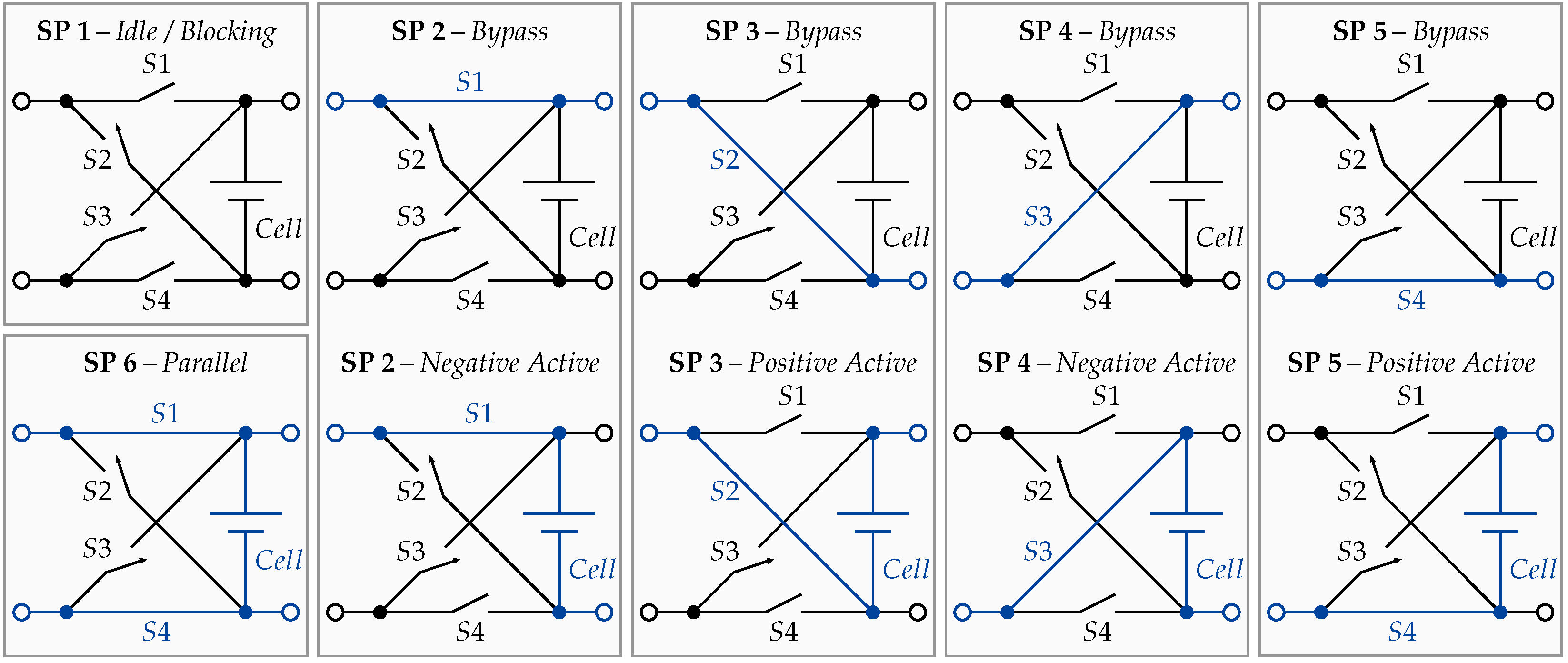
Within the PECIN topology, each current path fulfills multiple functions to realize the desired interconnection between the SMs. Figure 3 presents the SM switching pattern (SP) relevant for practical operation and the corresponding functional states of the SM. The figure further illustrates that the functional state of an SM depends not only on its own SP but also on those of the preceding and following SMs within the phase arm [13].
Selecting the appropriate switching technology is a key aspect of implementing the topology. In a single-cell configuration of the PECIN topology, each switching element must only be able to block the voltage of a single cell. However, both unidirectional and bidirectional blocking switching elements are required [12]. MOSFETs offer unidirectional blocking ability and are particularly suitable for this kind of application due to their high switching speed and low on-resistance [11]. A bidirectional blocking switch can be designed by arranging two single MOSFETs in a BtB configuration. Consequently, BtB MOSFETs exhibit nearly twice the on-resistance of a single MOSFET due to their antiserial connection.

3. PECIN SM Modeling

The modeling of the PECIN MLI employs a control-oriented approach to capture the system dynamics. This section focuses on the electrical and thermal characteristics of the PECIN topology at the SM level. Each SM contains a battery cell and four dedicated switching elements that define the topology’s switching network. Lithium-ion battery cells and a printed circuit board (PCB) implementation of the PECIN topology, as reported in previous studies [12,13], form the basis of the model. The PCB incorporates the MOSFETs and the power paths connecting the individual battery cells.
In the mathematical formulation, the Hadamard product, denoted by the ∘ operator, represents the element-wise multiplication of two matrices. This can be expressed as ( A B ) i j for every pair of indices i { 1 , 2 , , n } and j { 1 , 2 , , m } with n , m N , where A = [ a i j ] and B = [ b i j ] . Similarly, the element-wise division of the matrices, denoted by the symbol ⊘, is defined as ( A B ) i j = a i j / b i j , representing the Hadamard division. Additionally, the Hadamard power, denoted by the superscript ( · ) p , represents the element-wise exponentiation of a matrix, defined as A p = [ ( a i j ) p ] with p R . The Hadamard product, division, and power each have a time complexity of O ( n · m ) , which is the same as for matrix addition and subtraction of the matrices A and B . In this study, 0 n × m , 1 n × m , and  n × m represent matrices with all entries equal to zero, one, or infinity, respectively.

3.1. Electrical Battery Cell Model

In grid-connected and motor-drive applications of cascaded MLIs, the battery cells are typically charged and discharged using alternating current. Depending on the prevailing series-parallel configuration within each phase arm, the individual cell currents may be zero, a fraction of the phase arm current, or the entire phase current. The currents contain multiple harmonic components, with frequencies extending up to several kilohertz [25].
The SoC of the battery cells SoC R N S M × N P H , which quantifies the remaining cell capacity available at a given time, is directly related to the cell current I C e l l R N S M × N P H , as shown in the following equation, and has a significant impact on the electrical behavior.
SoC [ k + 1 ] = SoC [ k ] + h · η C , C e l l · Q C e l l 1 I C e l l [ k ]
The SoC is influenced by the cell capacity Q C e l l R N S M × N P H and the coulombic efficiency η C , C e l l R . This cell capacity describes the amount of charge that can be stored or extracted from a single battery cell. It is assumed that the capacity remains constant over the considered time horizon but may vary from cell to cell. The coulombic efficiency of lithium-ion cells is generally near unity [26,27], and thus, this study adopts a value of 1 for the coulombic efficiency. In the discrete-time representation of Equation (1) using the Euler approximation, the time step size is denoted by h = t k + 1 t k .
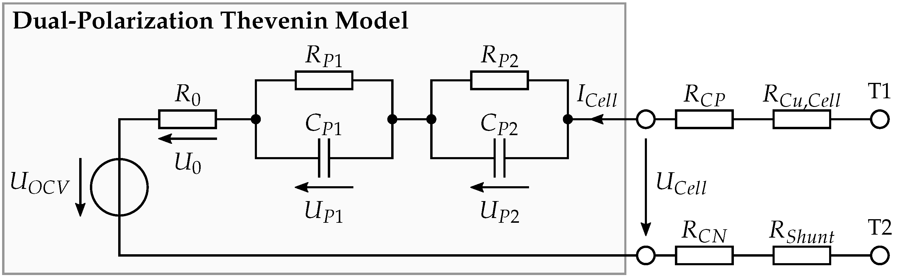
The electrical behavior of the battery cells with respect to the terminals is modeled using an equivalent circuit model, which includes a voltage source U O C V , a series resistor R 0 , and two RC elements ( N R C = 2 ) consisting of resistors R P 1 and R P 2 and capacitors C P 1 and C P 2 . The model known as the Dual-Polarization Thevenin Model (shown in Figure 4), is widely used because it provides a good balance between accuracy and the effort required for computation and parameterization [25,28,29,30].
The electrical circuit elements are usually not constant, but exhibit a nonlinear dependence on the cell’s SoC and core temperature T C e l l , C of the cell. This nonlinearity is represented by the look-up tables R 0 : R 2 R , R P n : R 2 R , C P n : R 2 R and U O C V : R 2 R with n = { 1 , 2 , , N R C } .
The voltages across the RC elements are called polarization voltages and represent the states of the electrical model. One RC element models electrochemical polarization, while the second captures concentration polarization. The polarization voltages U P n can be described in the continuous time domain using the differential equation
U ˙ P n = C P n 1 I C e l l ( R P n C P n ) 1 U P n f C e l l , P ( t , U P n ( t ) )
with the polarization resistance R P n R N S M × N P H and polarization capacitance C P n R N S M × N P H matrices. The time-discrete form of Equation (2) for numerical calculation is derived using the forward Euler method.
U P n [ k + 1 ] = U P n [ k ] + h · f C e l l , P ( k , U P n [ k ] )
Furthermore, the electrical time constants of the RC elements are given by
τ P n [ k ] = R P n [ k ] C P n [ k ] .
The voltage between the cell terminals U C e l l at time step k is calculated by adding the open-circuit voltage U O C V , the ohmic voltage drop U 0 , and the polarization voltages U P n .
U C e l l [ k ] = U O C V [ k ] + R 0 [ k ] I C e l l [ k ] + n = 1 N R C U P n [ k ]
The clamping behavior at the terminals T1 and T2 of the electrical circuit shown in Figure 4 at a given time step k can also be represented by a simplified equivalent circuit consisting of the voltage source U T , C e l l and the resistance R T , C e l l . This circuit transformation can be performed without any loss of accuracy and facilitates the subsequent circuit analysis of the PECIN MLI. The voltage matrix U T , C e l l is given by the sum of the open-circuit voltage and the polarization voltages.
U T , C e l l [ k ] = U O C V [ k ] + n = 1 N R C U P n [ k ]
The resistance R T , C e l l is composed of the internal cell resistance R 0 , the contact resistances R C P and R C N at the positive and negative cell terminal to the PCB, the copper trace resistance R C u , C e l l of the PCB and an optional shunt resistance R S h u n t for cell current measurement. The cell current information is usually required in MLIs with integrated battery cells to perform various balancing control strategies. The matrices R C P , R C N , and  R S h u n t are assumed to remain constant over time, but may represent different resistance values for each PECIN SM.
R T , C e l l [ k ] = R 0 [ k ] + R C u , C e l l [ k ] + R C P + R C N + R S h u n t

3.2. Thermal Battery Cell Model

The battery cells constitute an integral part of the inverter and have a significant impact on overall system performance. The cell temperature is also critical for safe and efficient operation, as the underlying physical and chemical processes are strongly influenced by the temperature. Due to the electrochemical interactions in lithium-ion cells, this is also reflected in the electrical behavior of the battery cells.
A widely established method for battery temperature modeling and estimation is based on thermal equivalent circuit models, such as Foster and Cauer networks [21,31,32,33]. This study employs an extended version of the Cauer model, as introduced by Schmid et al. [21], to describe the lumped thermal behavior of the battery cells. The model includes two states that represent the cell core temperature T C e l l , C and surface temperature T C e l l , S . Owing to its few states, the model is computationally efficient and well-suited for control-oriented applications [33]. In this modeling approach, the battery cell core and surface are modeled as a thermally homogeneous body characterized by effective thermal parameters and uniform internal heat generation. For further considerations, the model was expanded to include an additional state T C e l l , T that reflects the temperature of the copper connections used to contact the cell terminals. The extended thermal cell model is shown in Figure 5.
The thermal equivalent circuit contains three heat sources representing the losses in the battery cell P C e l l , the conduction losses in the copper connections P C u , C e l l at the cell terminals, and an additional heat source P E x t , C e l l accounting for external influences. The heat source P E x t , C e l l is used to model heat transfer of the MOSFETs as well as adjacent cells within a battery module. Furthermore, the thermal battery cell model is linked via P E x t , C e l l to the temperature distribution model described in Section 4.4. The thermal capacity C t h , C e l l , C is directly heated by the heat source P C e l l and linked to the surface temperature T C e l l , S via the thermal resistance R t h , C S . In addition, the surface temperature at the capacity C t h , C e l l , S is influenced by the heat source P E x t , C e l l and the heat input from the copper connections at the cell terminals, via the thermal resistance R t h , S T . The heat capacity C t h , C e l l , T defines the temperature of the copper connection and is linked to the ambient temperature T A via the resistance R t h , T A . The states of the thermal circuit are described using the following differential equations.   
T ˙ C e l l , C = C t h , C e l l , C 1 · P C e l l + R t h , C S 1 T C e l l , S T C e l l , C f C e l l , C ( t , T C e l l , C ( t ) )
T ˙ C e l l , S = C t h , C e l l , S 1 · P E x t , C e l l R t h , C S 1 T C e l l , S T C e l l , C + R t h , S T 1 T C e l l , T T C e l l , S f C e l l , S ( t , T C e l l , S ( t ) )
T ˙ C e l l , T = C t h , C e l l , T 1 · P C u , C e l l R t h , S T 1 T C e l l , T T C e l l , S + R t h , T A 1 T C e l l , T T A f C e l l , T ( t , T C e l l , T ( t ) )
The Equations (8)–(10) are numerically solved by discretizing them with the forward Euler method.
T C e l l , C [ k + 1 ] = T C e l l , C [ k ] + h · f C e l l , C ( k , T C e l l , C [ k ] )
T C e l l , S [ k + 1 ] = T C e l l , S [ k ] + h · f C e l l , S ( k , T C e l l , S [ k ] )
T C e l l , T [ k + 1 ] = T C e l l , T [ k ] + h · f C e l l , T ( k , T C e l l , T [ k ] )
The heat generation in a lithium-ion battery is modelled according to [21,33,34], considering the irreversible and reversible heat generation. Irreversible heat generation P R e s arises from ohmic losses in the cell, while reversible heat generation primarily results from entropy changes. The reversible heat generation is expressed by the term P E n t r , which includes the entropic heat coefficient c E n t r = U O C V / T C e l l , C . The entropic heat coefficient is represented by the look-up table C E n t r : R R , taking the SoC as input.
P C e l l [ k ] = R 0 [ k ] I C e l l 2 [ k ] + n = 1 N R C U P n [ k ] I C e l l [ k ] P R e s [ k ] + c E n t r [ SoC [ k ] ] · T C e l l , C [ k ] I C e l l [ k ] P E n t r [ k ]
The heat generation resulting from ohmic conduction losses in the copper connections is calculated according to Equation (15). The total ohmic resistance consists of several components, including the copper resistance R C u , C e l l , the contact resistances R C P and R C N , and a potential shunt resistance R S h u n t used for cell current measurement.
P C u , C e l l [ k ] = R C u , C e l l [ k ] + R C P + R C N + R S h u n t I C e l l 2 [ k ]
The typically low temperature coefficient of the resistance component R S h u n t allows it to be treated as constant across the operating temperature range. However, in the case of the copper resistances, a linear temperature dependence with
R C u , C e l l [ k ] = R C u , C e l l , 0 1 N S M × N P H + α C u · T T , C e l l [ k ] T C u , 0 · 1 N S M × N P H .
is considered, where α C u represents the temperature coefficient of copper and R C u , C e l l , 0 designates to the copper resistance at the reference temperature T C u , 0 . The resistance R C u , C e l l , 0 may vary across cells.

3.3. Electrical MOSFET and PECIN Trace Model

In control-oriented modeling of the PECIN MLI, the primary focus is on the high-level dynamics of the switching system. These dynamics are predominantly governed by the steady-state electrical behavior of the single and BtB MOSFETs. Consequently, detailed modeling of the transient switching behavior is not pursued. To reduce model complexity, an accurate representation of the idle/blocking state is also omitted. In this switching state, the anti-parallel body diodes of the single MOSFETs establish the current path. The conduction of the body diodes, either S 2 and T U 1 or S 3 and T U 2 , is determined by the magnitude and sign of the voltage between the terminals L and N of each phase arm. To accurately capture the system dynamics and represent the static switching characteristics, this study employs a non-ideal switch model based on the switched resistor technique.
In this approach, switching elements are modeled as resistors with resistance dependent on the switching state. The states of the switches within the SMs S x { S 1 , S 2 , S 3 , S 4 } and the Termination Unit T U x { T U 1 , T U 2 } of each phase arm are defined via Sx = [ S x i , j ] B N S M × N P H and TUx = [ T U x i , j ] B 1 × N P H . For the indicies i { 1 , 2 , , N S M } and j { 1 , 2 , , N P H } and the set B { 0 , 1 } apply. A switch state of 1 denotes the on-state, and 0 denotes the off-state.
Single and BtB MOSFETs are modeled by their on-state resistance R D S , o n and a nearly infinite off-state resistance R F e t , o f f (e.g., 10 20   Ω ). For switching elements implemented as BtB MOSFETs, twice the resistance of a single MOSFET is assumed. This condition is mathematically expressed in Equation (17) through the number of serial MOSFETs N F e t , S e r using the indicator function I . The indicator function I S x { S 1 , S 4 } equals 1 if S x belongs to the set { S 1 , S 4 } , and 0 if S x does not belong to the set. The parallel arrangement of multiple discrete MOSFETs per switching element is accounted for by the number of parallel MOSFETs N F e t , P a r N . The on-resistances at time step k of all MOSFET-based switches are given by the matrices R D S , o n , S x and R D S , o n , T U x , whereas R F e t , S x and R F e t , T U x characterize the resistances of the overall switching elements.
N F e t , S e r = 1 + I S x { S 1 , S 4 } N
R F e t , S x [ k ] = N F e t , S e r · N F e t , P a r 1 · R D S , o n , S x [ k ] R N S M × N P H
R F e t , T U x [ k ] = N F e t , S e r · N F e t , P a r 1 · R D S , o n , T U x [ k ] R 1 × N P H
In addition to the resistances assigned to the MOSFETs, the resistances of the electrical interconnections are also considered. Most of the additional resistance is attributable to the copper interconnections [35]. Minor resistance components that are not caused by copper, such as those arising from solder joints, are considered negligible due to their short length and comparatively large cross-sectional area. The matrices R C u , S x [ k ] = [ R C u , S x , i , j [ k ] ] R N S M × N P H and R C u , T U x [ k ] = [ R C u , T U x , i , j [ k ] ] R 1 × N P H assign a copper resistance to each electrical path in the PECIN topology, which is in series with the resistances R F e t , S x and R F e t , T U x , respectively. For the subsequent electrical analysis of a PECIN MLI in Section 4, the MOSFET and copper resistances are merged into trace resistances. The trace resistance matrices R T , S x and R T , T U x characterize the electrical resistance of each current path within the PECIN MLI. Equations (20) and (21) express the relationship between the trace resistances and the switching states Sx and TUx at time step k.
R T , S x [ k ] = Sx [ k ] R F e t , S x [ k ] + R C u , S x [ k ] + ¬ Sx [ k ] · R F e t , o f f
R T , T U x [ k ] = TUx [ k ] R F e t , T U x [ k ] + R C u , T U x [ k ] + ¬ TUx [ k ] · R F e t , o f f

3.4. Thermal MOSFET and PECIN Trace Model

Although the electrical behavior of MOSFETs in the on-state can be well represented by the resistance R D S , o n , the resistance in inverter operation is typically not constant but varies with the MOSFET junction temperature. The same applies to the copper resistance, which is dependent on the PCB temperature. Consequently, variations in MOSFET and copper resistances affect current distribution within and between the phase arms.
To capture this effect, a thermal network based on a Cauer model (see Figure 6) is employed to describe the dynamic thermal behavior of the MOSFETs and PCB traces. The Cauer model approach is specifically chosen for its ability to represent how temperature changes within the system influence the electrical resistances, directly linking each model node to a specific physical temperature point.
The thermal model includes the heat source P F e t , which represents MOSFET losses, P C u for copper losses in the electrical connections to the MOSFET, and  P E x t , F e t as the external heat source. The external heat source represents the heat transfer from the battery cells and other current paths within the PECIN topology (see Section 4.4). The junction thermal capacity C t h , F e t , J is heated by the thermal source P F e t and is thermally coupled to the MOSFET case temperature via the resistance R t h , J C . The heat capacity C t h , F e t , C of the casing is additionally connected to both heat sources P C u and P E x t , F e t via the thermal resistance R t h , C T . The temperature of the electrically conductive current path on the PCB for the practical implementation of the PECIN topology is defined by the heat capacity C t h , P C B , T . Additionally, the PCB’s thermal potential is linked to the ambient temperature T A via the resistance R t h , T A .
The thermal model comprises three states: MOSFET junction temperature T F e t , J , MOSFET case temperature T F e t , C , and PCB trace temperature T P C B , T . Based on the proposed thermal model, the differential Equations (22)–(24) for the MOSFET junction temperature, the MOSFET case temperature, and the PCB trace can be formulated. Since the following equations refer to all switches S x and T U x , the explicit index has been omitted.
T ˙ F e t , J = C t h , F e t , J 1 · P F e t R t h , J C 1 T F e t , J T F e t , C f F e t , J t , T F e t , J ( t )
T ˙ F e t , C = C t h , F e t , C 1 · R t h , J C 1 T F e t , J T F e t , C R t h , C T 1 T F e t , C T P C B , T f F e t , C ( t , T F e t , C ( t ) )
T ˙ P C B , T = C t h , P C B , T 1 · P C u + P E x t , F e t + R t h , C T 1 T F e t , C T P C B , T R t h , T A 1 T P C B , T T A f P C B , T ( t , T P C B , T ( t ) )
The time-discrete formulation of the Equations (22)–(24) is obtained by applying the forward Euler method.
T F e t , J [ k + 1 ] = T F e t , J [ k ] + h · f F e t , J k , T F e t , J [ k ]
T F e t , C [ k + 1 ] = T F e t , C [ k ] + h · f F e t , C k , T F e t , C [ k ]
T P C B , T [ k + 1 ] = T P C B , T [ k ] + h · f P C B , T k , T P C B , T [ k ]
Within the proposed simulation framework, this thermal model is used to calculate the temperatures T F e t , J , T F e t , C , and  T P C B , T for every single and BtB MOSFET switch. The heat capacities C t h , F e t , J , C t h , F e t , C , and  C t h , P C B , T , as well as the thermal resistances R t h , J C , R t h , C T , and  R t h , T A , are assumed to be time-invariant but may vary for each switching element.
The heat sources P F e t , S x and P C u , S x , corresponding to the instantaneous losses in the MOSFETs and copper traces of the switches S x , are computed using Equations (28) and (29). Here, I x where x { 1 , 2 , 3 , 4 } denotes the current in the path associated with corresponding switch S x . The equations for the switches T U x are derived analogously and are omitted for brevity.
P C u , S x [ k ] = R C u , S x [ k ] I x [ k ] 2
P F e t , S x [ k ] = R D S , o n , S x [ k ] N F e t , P a r 1 · I x [ k ] 2
Previous investigations have demonstrated that conduction losses dominate the total MOSFET losses, while switching losses represent only a minor contribution in cascaded MLIs [7,8]. Accordingly, this study is restricted to MOSFET conduction losses in order to represent the heat generation within the MOSFET switching elements. The omission of switching losses, gate driver losses, conduction losses in the body diode, and leakage currents also results in slightly underestimated temperatures.
The on-resistances of the MOSFETs R D S , o n , S x and R D S , o n , T U x exhibit temperature dependence and vary with the junction temperatures T F e t , J , S x and T F e t , J , T U x . The nonlinear temperature dependence of the on-resistances is characterized using the look-up table R D S , o n : R R , with the junction temperatures as inputs. The data is extracted from the MOSFET datasheet [36]. For the copper trace resistances R C u , S x and R C u , T U x , a linear temperature dependence on T P C B , T , S x and T P C B , T , T U x is assumed. The corresponding mathematical formulation follows Equation (16), where R C u , S x , 0 and R C u , T U x , 0 denote the nominal copper trace resistance at the reference temperature T C u , 0 and may differ between individual traces.

4. PECIN MLI Modeling

The structure of a PECIN MLI represents a complex electrical network due to the large number of switching elements. Efficient network analysis is essential for developing a high-performance inverter model, as it enables the simulation of multiple SMs and phases, while also addressing the frequent computational demands.
The straightforward application of standard methods for analyzing electrical networks, such as the mesh current or nodal voltage method, would involve a computationally intensive matrix inversion. The computational complexity of matrix inversion scales cubically ( O ( N 3 ) ) with the number N of independent nodes or meshes in the network.
According to the Thevenin equivalent circuit described in Section 3.1, each battery cell at time step k is modeled as a voltage source in series with a resistance, whose values are given by the matrices U T , C e l l and R T , C e l l . Based on this representation, each PECIN SM comprises three independent nodes and three independent meshes. The Termination Unit within each phase arm introduces an additional node and mesh. For  N P H phase arms, the total number of independent nodes and meshes is given by N P H · ( 3 · N S M + 1 ) , while further meshes and nodes emerge at the system level due to the interconnection and coupling of an external source or load. As a result, even PECIN MLIs with a relatively small number of SMs require considerable computing effort.
The following Sections introduce an approach for electrical network analysis of a PECIN MLI with reduced time complexity, as well as a temperature distribution model for PECIN modules to capture thermal interactions between the integrated components.

4.1. Electrical Modeling of the PECIN Phase Arms

A PECIN MLI generally consists of structurally identical phase arms. Each phase arm incorporates the same number of SMs, with a Closing and Termination Unit located at the phase terminals N and L. The electrical modeling of the battery cells and the individual PECIN traces has already been addressed in Section 3.1 and Section 3.3. Building on this foundation, the modeling of the individual phase arms is presented in the following.
Each phase arm consists of an equivalent electrical network that incorporates the voltage sources U T , C e l l and resistances R T , C e l l associated with the battery cell current paths, as well as the trace resistances R T , S x and R T , T U x , as illustrated in Figure 7. The currents within an SM are given by I x and I C e l l , trace currents within the Closing Unit by I C U 1 and I C U 2 , and those within the Termination Unit by I T U 1 and I T U 2 .
The electrical behavior of each phase arm with respect to the terminals L and N can be represented by a simplified Thevenin equivalent circuit comprising the resistance R E q R 1 × N P H and voltage U E q R 1 × N P H matrices. The resistance matrix R E q is determined through successive electrical circuit transformations, including series-parallel combinations as well as star-delta and delta-star transformations, with the voltage sources U T , C e l l treated as short circuits.
Throughout the transformation, additional resistance matrices are calculated and used to derive the equivalent voltage U E q and to compute the current distribution within each phase arm, as outlined in Section 4.3. As the cascaded structure of each PECIN MLI phase arm is the same, all calculations are executed concurrently using element-wise operations.
For mathematical notation, the functions T Y Δ ( R A , R B , R C ) = ( R A B , R B C , R A C ) for the star-delta transformation and T Δ Y : ( R A B , R B C , R A C ) = ( R A , R B , R C ) for the delta-star transformation, are introduced in the following Equations (30)–(33).
R Σ 1 = R A R B + R B R C + R C R A R 1 × N P H
R Σ 2 = R A B + R B C + R A C R 1 × N P H
T Y Δ ( R A , R B , R C ) = R Σ 1 R C , R Σ 1 R A , R Σ 1 R B
T Δ Y ( R A B , R B C , R A C ) = ( R A B R A C R Σ 2 , R A B R B C R Σ 2 , R B C R A C R Σ 2 )
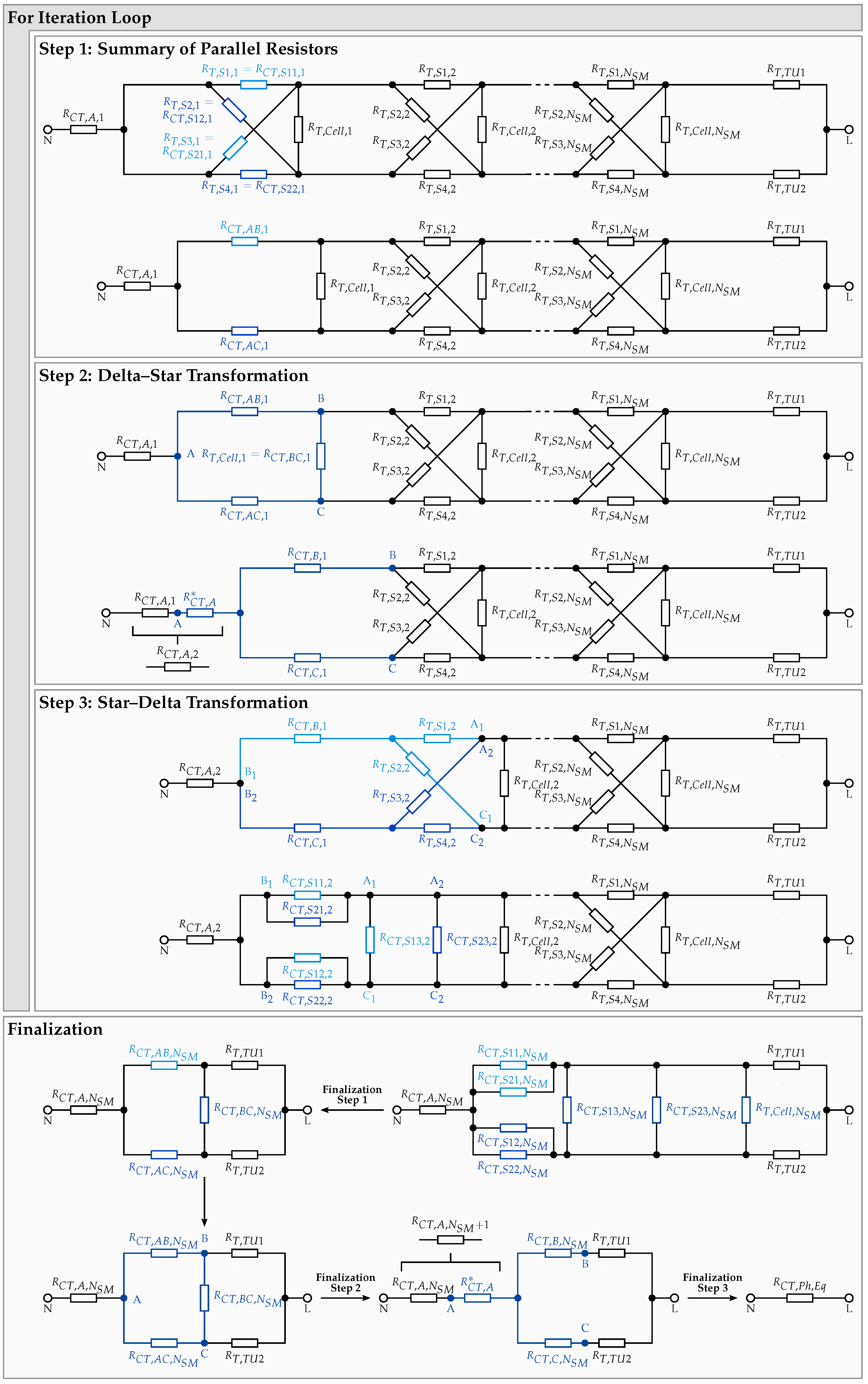
The algorithm developed to execute the successive transformations of the PECIN phase arm electrical network is described below. For clarity, the procedure is decomposed into two sub-algorithms, each addressing a distinct propagation direction within the network.
The first part of the algorithm initiates from the Closing Unit and calculates the equivalent resistance matrices R C T , m , R C T , n , R C T , o up to the Termination Unit at the other end of the phase arm. In contrast, the second algorithm part starts at the Termination Unit and computes the equivalent resistance matrices R T C , m , R T C , n , R T C , o , up to the Closing Unit. For the indices, it holds that m { A , B , C } , n { A B , A C , B C } and o { S 11 , S 12 , S 13 , S 21 , S 22 , S 23 } . For  l { C T , T C } , n A , and  o { S 13 , S 23 } , the matrices R l , m , R l , n , and  R l , o belong to R N S M × N P H . In contrast, R l , A R ( N S M + 1 ) × N P H , and for each o { S 11 , S 12 , S 21 , S 22 } , R T C , o R ( N S M 1 ) × N P H .
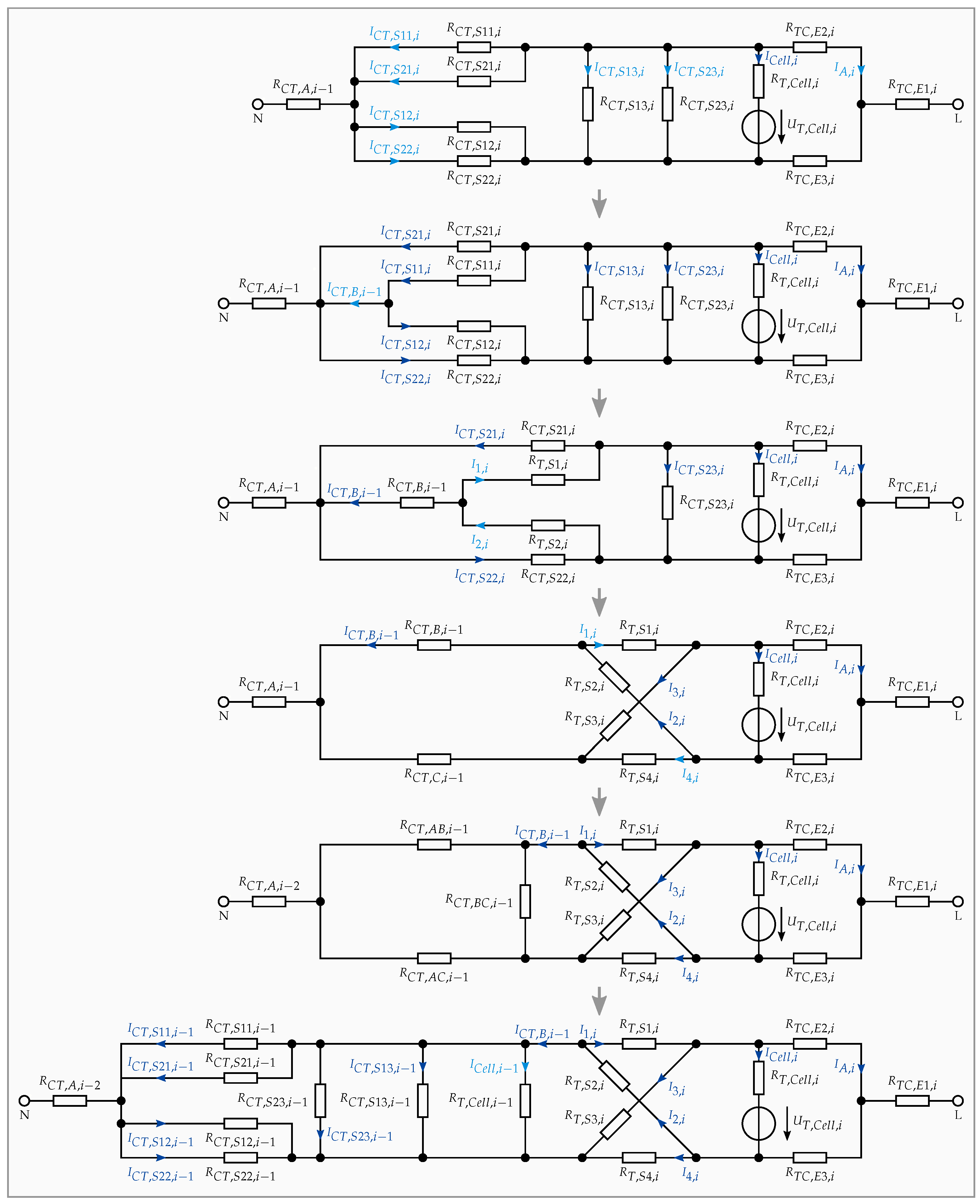
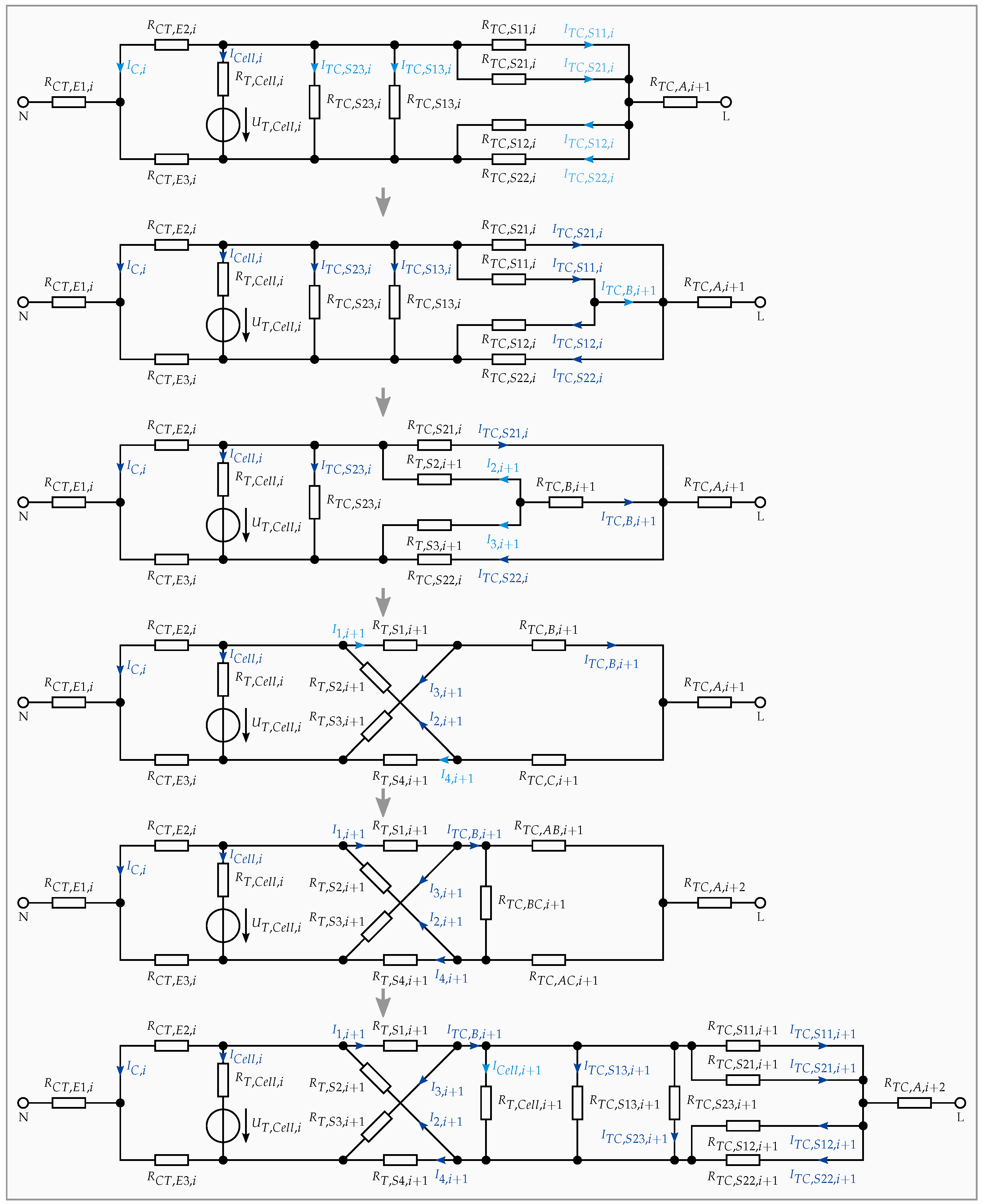
The first algorithm part is detailed in Algorithm 1, with its underlying functional principle depicted in Figure 8. The main iteration loop in Algorithm 1 consists of three essential transformation steps executed sequentially in a repetitive cycle. The iteration counter x, ranging from 1 to N S M 1 , also serves as a subscript for the resistance matrices, thereby indicating the corresponding row index of the matrices. After completion of the iteration loop, the algorithm concludes with the final steps to calculate the remaining resistance entries in the matrices, as well as the equivalent resistances of the phase arms. As all phase arms are computed simultaneously, the column index j { 1 , 2 , , N P H } is omitted from the subscript. The algorithm incrementally construct the resistance matrices R C T , m , R C T , n , and  R C T , o and concludes with the computation of the resistance of each phase arm R C T , P h , E q . The electrical circuit diagrams in Figure 8 illustrate the sequential network transformations, with the corresponding resistances highlighted in each step.
Algorithm 1: PECIN Equivalent Resistance Calculation from the Closing Unit to the Termination Unit
Batteries 12 00181 i001
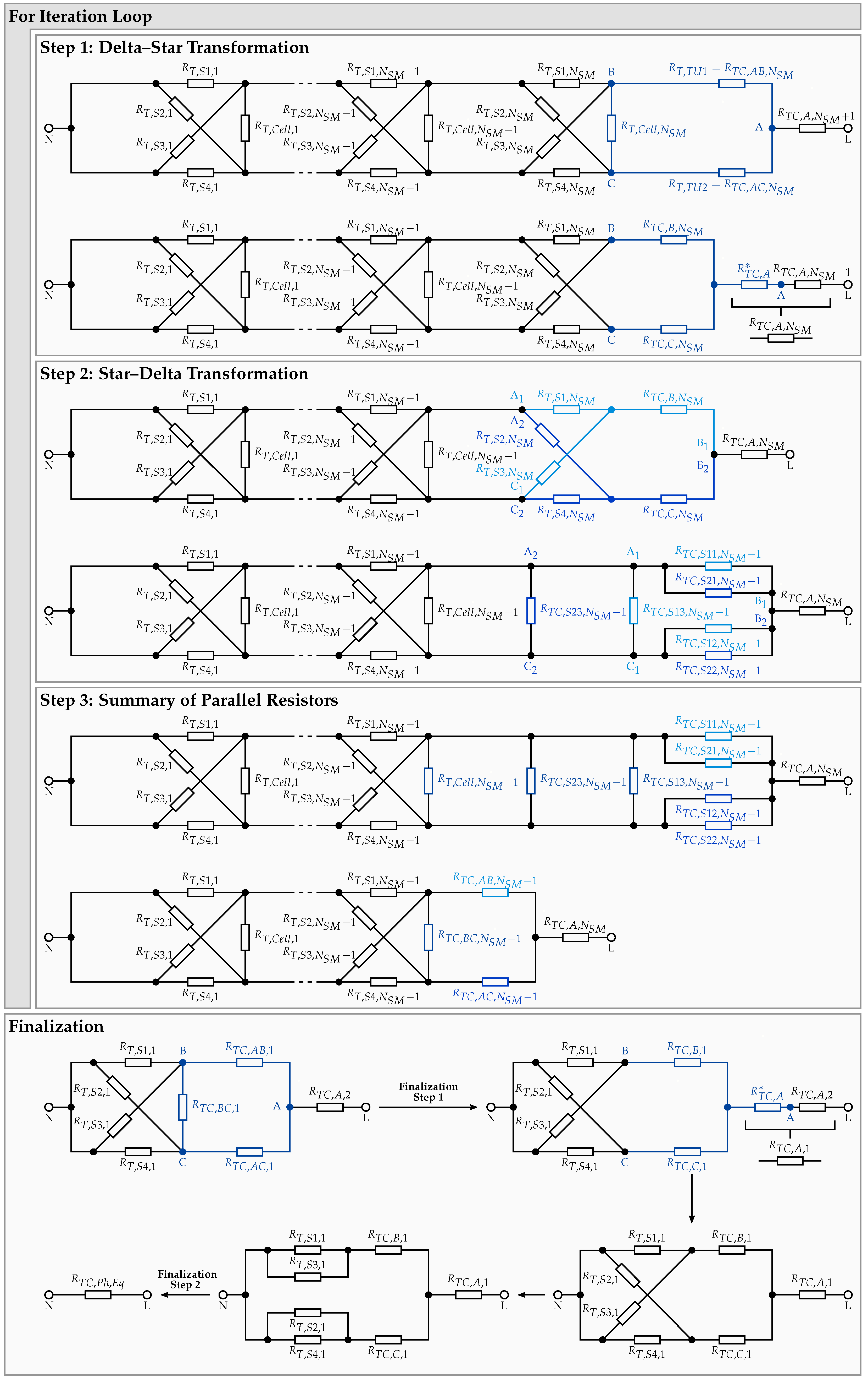
The second algorithm part, featuring the opposite propagation direction, is presented in Algorithm 2 and illustrated in Figure 9. The loop iteration index, given by y = N S M + 1 x , is employed to construct the resistance matrices R T C , m , R T C , n , and  R T C , o consistently with the first algorithm part, thereby facilitating subsequent computations.
The main iteration loops in Algorithms 1 and 2 can be executed sequentially or combined into a single for loop, using the iteration index x or y. Each algorithm requires a total of N S M 1 loop iterations, followed by a set of finalization steps to traverse the entire electrical network once, leading to a computational complexity of O ( N S M ) .
Algorithm 2: PECIN Equivalent Resistance Calculation from the Termination Unit to the Closing Unit
Batteries 12 00181 i002
The resistance matrices R C T , P h , E q and R T C , P h , E q represent both the resistance of all phase arms and differ only marginally due to limited numerical precision. To reduce numerical errors, the resulting equivalent resistance is taken as the average of both resistances.
R E q = 1 2 · R C T , P h , E q + R T C , P h , E q
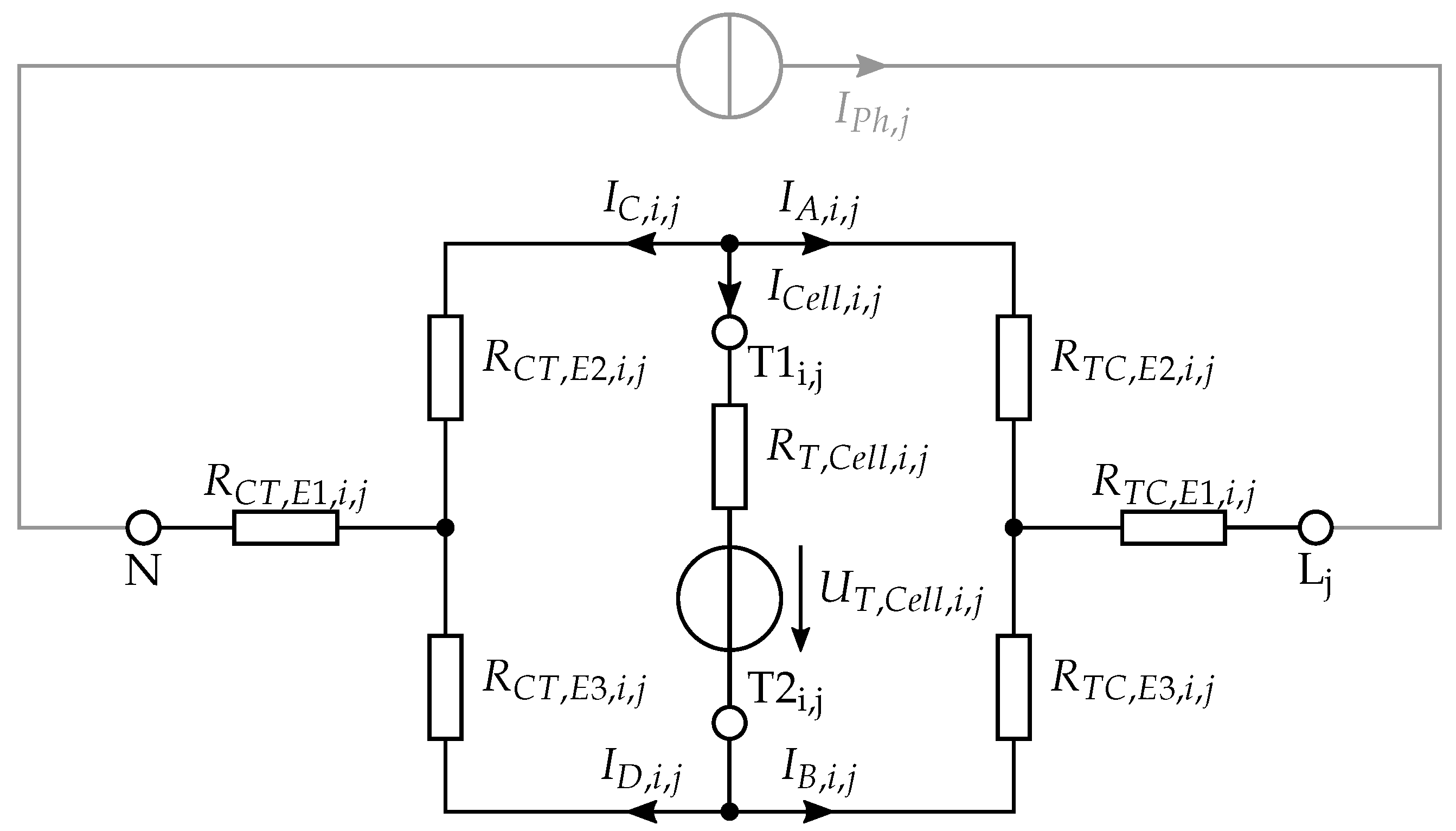
Along with the resistance R E q , the voltage U E q must be determined to fully characterize the terminal behavior of each phase arm using a Thevenin equivalent. Based on the applied circuit transformations, a uniform equivalent circuit diagram for each SM within a phase arm is derived. The resulting diagram, shown in Figure 10, facilitates the calculation of the equivalent voltage U E q using the superposition theorem.
The equivalent circuit illustrates the electrical relationship between the terminals of a single battery cell within an SM and the overall terminal behavior of the phase arm. Additionally, it highlights the structural similarity between the PECIN topology and a Wheatstone bridge configuration. The current source, connected between the phase terminals N and L, represents the instantaneous phase current when the PECIN phase arm is coupled with an external source or load. The resistances within the electrical circuit can be calculated using the Equations (35)–(38).
R C T , P = R C T , S 13 1 + R C T , S 23 1 1
R T C , P = R T C , S 13 1 + R T C , S 23 1 1
T Δ Y ( R C T , A B , R C T , P , R C T , A C ) = R C T , E 1 , R C T , E 2 , R C T , E 3
T Δ Y ( R T C , A B , R T C , P , R T C , A C ) = R T C , E 1 , R T C , E 2 , R T C , E 3
Using the equivalent circuit, the voltage potential at the N and L terminals for each SM can be determined from Equations (39)–(42). In this analysis, the current source is treated as an open circuit. The equivalent voltage U E q is obtained as the difference between the voltage potentials, with the contributions of all SMs superimposed.
K = R C T , E 2 + R C T , E 3 ( R T C , E 2 + R T C , E 3 )
U N = R C T , E 3 U T , C e l l R T , C e l l ( 1 N S M × N P H + K ) + R C T , E 2 + R C T , E 3
U L = R T C , E 3 U T , C e l l R T , C e l l ( 1 N S M × N P H + K 1 ) + R T C , E 2 + R T C , E 3
U E q = i = 1 N S M U L , i U N , i
Based on the electrical circuit shown in Figure 10, the resistance seen by the battery cells between T1i,j and T2i,j with respect to the phase-arm connection can be calculated using Equation (43). In this context, the current source is regarded as an open circuit.
R E , C e l l = R C T , E 2 + R C T , E 3 1 + ( R T C , E 2 + R T C , E 3 ) 1 1

4.2. Electrical Modeling of the Overall System

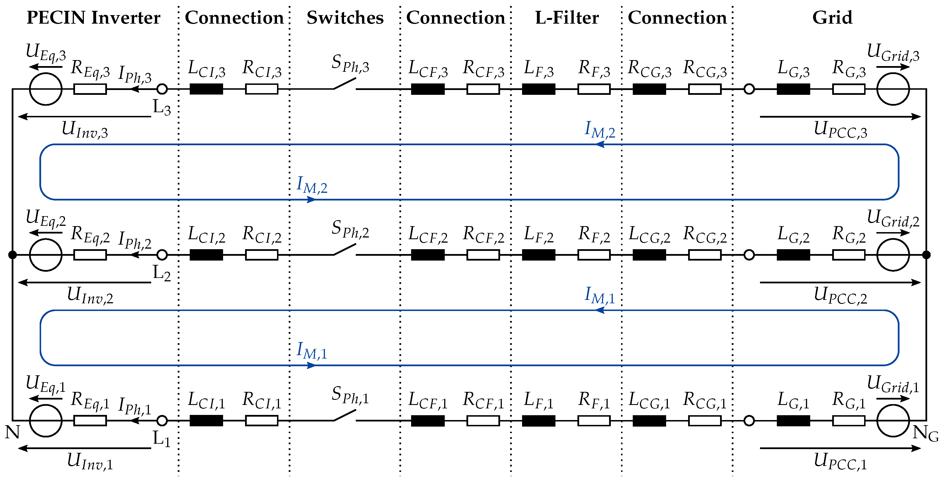
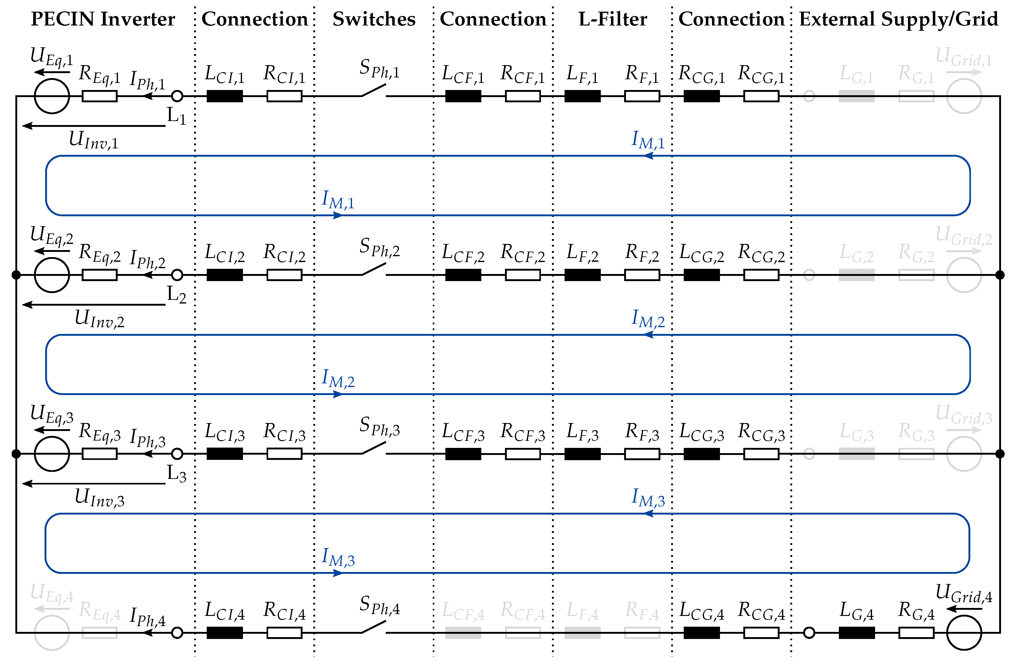
The system-level electrical circuit employed in this study is capable of simulating the PECIN MLI under various AC and DC charging configurations. Accordingly, the electrical circuit depicted in Figure 11 comprises an inverter, a filter and a grid model.
The electrical model of the PECIN MLI consists of multiple phase arms, each modeled with the voltage source U E q , j in series with the resistance R E q , j , as described in Section 4.1. In Figure 11, three individual phase arms ( N P H = 3 ) are connected in a star configuration with a common neutral point.
To ensure grid operation in accordance with recommended standards [37] for harmonics in current and voltage at the point of common coupling (PCC), an additional filter is generally required. Passive L, LC, or LCL grid filters are commonly employed in grid-connected inverters [38,39,40]. Therefore, each phase incorporates an L-filter, modeled using the inductances L F , j and resistances R F , j .
The utility grid is comparable to the PECIN MLI, represented by a Thevenin equivalent model, comprising a voltage source U G r i d , j and a resistive-inductive impedance for each phase. The grid impedance is characterized by the grid resistance R G , j and the grid inductance L G , j . Based on the impedance being considered, both weak and strong grid conditions can be studied.
The additional switching elements S P h , j in each phase are used to connect or disconnect the inverter from the grid. It is assumed that all switching elements S P h , j maintain the same state at all times. This electrical circuit configuration thus also facilitates the investigation of transient processes during the start-up phase of grid operation, when the inverter’s phase voltages are not yet synchronized with the grid voltages in terms of amplitude, frequency, and phase angle. The electrical interconnections between the individual components are considered via the resistances R C I , j , R C F , j , R C G , j and the inductances L C I , j , L C F , j , L C G , j .
By adjusting the number of phases N P H and the parameters of the individual sources and passive components, the electrical circuit can be configured for a variety of AC and DC charging applications. An alternative circuit configuration is provided in Appendix A.
The resistance vectors R G , R F , R C I , R C F , R C G and the inductance vectors L G , L F , L C I , L C F , L C G summarize the resistances and inductances of the grid, filter, and electrical interconnections. These elements are assumed to be constant over time but may differ between phases. In contrast, the elements of the resistance vector R E q and the voltage vectors U E q and U G r i d vary with both time and phase. All vectors have a dimension of 1 × N P H and are combined as follows to facilitate further analysis.
R E = R E q + R C I + R C F + R F + R C G + R G
L E = L C I + L C F + L F + L C G + L G
U E = U G r i d U E q
With regard to the phase currents, an open-state configuration of all switching elements S P h , j eliminates any conductive path between the phases, and it directly follows that I P h = 0 1 × N P H . A circuit interruption can also be induced by the switching elements within the PECIN MLI. Accordingly, the current I P h , j = 0 through the phase arm j is interrupted if one or more SMs within the respective phase arm are in the idle switching state. To ensure a closed circuit between phases, at least two PECIN phase arms must not be in the idle state, otherwise I P h = 0 1 × N P H would apply. It is further assumed that, for an open circuit, I ˙ P h = 0 1 × N P H , and for a PECIN phase arm j in the idle state, I ˙ P h , j = 0 . These assumptions are made to exclude transient effects arising from the switched-resistor modeling, which do not correspond to physical behavior.
As a result, the applied mesh current method for electrical network analysis only considers cases with a closed electrical system circuit. The analyzed meshes are defined between adjacent phases that do not contain SMs in the idle state. Figure 11 presents the mesh configuration of the standard operating case, in which all PECIN SMs operate in either bypass, parallel, or positive/negative active switching state. This approach decreases the dimensionality of the matrix-vector operations, reducing the computational effort and preventing numerical instabilities caused by phase resistances approaching infinity when solving the following differential equation.
I ˙ M = L 1 · ( R · I M + U ) f I ( t , I M ( t ) )
The numerical stability depends on the eigenvalues λ of the differential equation, which are linked via the characteristic polynomial det ( A λ I ) = 0 and A = L 1 · R with the matrices R and L . The time discretization of Equation (47) is performed using the forward Euler method.   
I M [ k + 1 ] = I M [ k ] + h · f I ( k , I M [ k ] )
For the inductance matrix L , the resistance matrix R , and the voltage vector U applies L , R R N M C × N M C and U R N M C × 1 . The number of independent meshes considered at time step k is denoted by N M C { 1 , 2 , , N P H 1 } . For the sake of simplicity, the explicit time dependence indicated by the index k for N M C and consequently L , R , and  U is omitted. For the case under consideration with N P H = 3 , the matrices R and L therefore vary in dimension only between 2 × 2 and 1 × 1 . The general structure of the tridiagonal matrices L and R for any N M C is shown below.
L = L E , 1 * + L E , 2 * L E , 2 * 0 0 L E , 2 * L E , 2 * + L E , 3 * L E , 3 * 0 0 L E , 3 * L E , 3 * + L E , 4 * 0 0 0 L E , N M C * L E , N M C * + L E , N M C + 1 *
R = R E , 1 * + R E , 2 * R E , 2 * 0 0 R E , 2 * R E , 2 * + R E , 3 * R E , 3 * 0 0 R E , 3 * R E , 3 * + R E , 4 * 0 0 0 R E , N M C * R E , N M C * + R E , N M C + 1 *
The matrix elements of L and R are defined using the auxiliary vectors R E * , L E * , U E * R 1 × ( N M C + 1 ) , which comprise only those elements of R E , L E , and  U E corresponding to phases with potentially non-zero phase currents. The voltage vector U is given by
U = M · U E * .
The auxiliary matrix M is defined as follows.
M = 1 1 0 0 0 1 1 0 0 0 1 1 R N M C × ( N M C + 1 )
The mesh current vector I M is transformed into the corresponding phase current vector I P h * using Equation (53). The same transformation can also be applied to the mesh current derivative I ˙ M to obtain the phase current derivative I ˙ P h * .
I P h * = M · I M
The vectors I P h * and I ˙ P h * contain only the phase currents or their time derivatives for phases represented in R E * , L E * , and  U E * . To reconstruct the phase current vector I P h R 1 × N P H and its time derivative I ˙ P h R 1 × N P H , the elements of I P h * and I ˙ P h * are assigned to their corresponding indices in I P h and I ˙ P h . Subsequently, the inverter output voltages U I n v and the voltage at the point of common coupling U P C C can be determined.
U I n v [ k ] = U E q [ k ] + R E q [ k ] I P h [ k ]
U P C C [ k ] = U G r i d [ k ] R G I P h [ k ] L G I ˙ P h [ k ]

4.3. Current Distribution Within the PECIN Phase Arms

Once the individual phase currents are determined, the next objective is to evaluate the current distribution within each phase arm. Methods such as the mesh current method and node potential analysis would involve high-dimensional matrix inversions. To circumvent the complexity of these operations, the superposition principle is applied, enabling most calculations to be performed using element-wise matrix operations. Additionally, the previously computed equivalent resistance matrices from the phase-arm Thevenin equivalent transformation are used to reduce the computational effort.
The independent analysis of current and voltage sources also facilitates the partial parallelization of arithmetic operations and provides additional insights into the contribution of each individual source to the overall current distribution. The superposition principle requires the consideration of the voltage sources U T , C e l l and the current sources I P h . The voltage sources are assigned to the respective cells within the phase arm, whereas the current sources reflect the influence of an external load or supply.
Initially, the impact of the instantaneous phase current on the individual trace and cell currents within each phase arm is analyzed, while the voltage sources are treated as short circuits. The electrical circuit, illustrated in Figure 10, serves as the basis for this analysis. The respective currents of the equivalent circuits for all SMs are summarized in the matrices I A , I B , I C , I D , and  I C e l l , each with dimensions N S M × N P H . For the current calculation, the electrical circuit is first transformed using the delta-star transformation, in accordance with Equations (56) and (57).
T Δ Y ( R T C , E 2 , R T , C e l l , R T C , E 3 ) = R T C , E A , R T C , E B , R T C , E C
T Δ Y ( R C T , E 2 , R T , C e l l , R C T , E 3 ) = R C T , E A , R C T , E B , R C T , E C
Subsequently, based on Kirchhoff’s current law, the current matrices are given by
I A = R C T , E C + R T C , E 3 R C T , E B + R T C , E 2 + R C T , E C + R T C , E 3 1 N S M × 1 · I P h ,
I B = 1 N S M × 1 · I P h I A ,
I C = R C T , E 3 + R T C , E C R C T , E 2 + R T C , E B + R C T , E 3 + R T C , E C 1 N S M × 1 · I P h ,
I D = 1 N S M × 1 · I P h I C .
The matrices I A and I B correspond to the currents at the cell-side terminals of all PECIN SMs. Owing to the cascaded arrangement of the SMs, the currents I A , i and I B , i of SMi are identical to those at the switching terminals of the subsequent SMi+1 within each phase. The currents at the cell-side terminals of the N S M -th SM directly correspond to the currents in the Termination Unit, with  I T U 1 I P h = I A , N S M and I T U 2 I P h = I B , N S M . The superscript ( · ) I P h indicates that the corresponding variable represents the contribution of the current sources associated with the phase currents. In contrast, the matrices I C and I D describe the currents from the battery cell to the switch network within each SM. Kirchhoff’s voltage and current laws are applied to determine the trace and cell currents, with Equations (62)–(66) providing the mathematical relationships.
I C e l l I P h = I B + I D
I 1 I P h = S · R T , C e l l I C e l l I P h R T , S 3 I C R T , S 1 + R T , S 3
I 2 I P h = R T , C e l l I C e l l I P h + R T , S 1 I 1 I P h R T , S 2
I 3 I P h = I C + I 1 I P h
I 4 I P h = I D + I 2 I P h
In Equation (63), the shift auxiliary matrix S is employed to define an equation based on Kirchhoff’s voltage law between adjacent SMs and to account for SM1, which directly interfaces with the Closing Unit. The matrix S performs a one-step downward shift of matrix elements and is defined as   
S = 0 0 1 0 0 0 1 0 0 0 0 1 0 R N S M × N S M .
Following the calculation of the phase current contribution, the individual current contributions of the N S M voltage sources U T , C e l l in each phase arm are subsequently determined. For this analysis, the current sources I P h are treated as open circuits, while each voltage source is considered independently and all remaining sources are replaced by short circuits. The individual current contributions are obtained using an iterative algorithm that successively applies reverse transformations to the electrical network of the condensed phase arm. By applying Kirchhoff’s voltage and current laws, along with Ohm’s law, the desired currents are determined in a stepwise manner. To eliminate redundant calculations, the algorithm incorporates the resistance matrices R C T , A B , R C T , A C , R T C , A B , R T C , A C , R C T , o , and  R T C , o , which are obtained using Algorithms 1 and 2.
Similar to the algorithms for calculating the equivalent resistances of the phase arms, the algorithm for calculating the current contributions employs two opposite iteration directions, presented separately in Algorithms 3 and 4. For methodological clarity, the calculation of auxiliary currents is separated from the primary objective of determining the trace and cell current contributions. The auxiliary currents serve only as intermediate results that facilitate the calculation of the cell current contribution I C e l l U T , C e l l , x and trace current contributions I N T U T , C e l l , x with N T { 1 , 2 , 3 , 4 } . The superscript ( · ) U T , C e l l , x denotes that the contributions are associated with the voltage sources U T , C e l l , x .
Algorithm 3: Current Contribution originating from U T , C e l l , x to subsequent SMs
Batteries 12 00181 i003
Algorithm 4: Current Contribution originating from U T , C e l l , x to preceding SMs
Batteries 12 00181 i004
The first part of the algorithm is presented in Algorithm 3, while the fundamental reverse transformation scheme in this direction is illustrated in Figure 12. The circuit transformation starts at SMx, including the voltage sources U T , C e l l , x , where x { 1 , 2 , , N S M } , and proceeds toward the Termination Units. Throughout the process, the consolidated electrical network is reconstructed sequentially, restoring it to its initial configuration.
In Algorithm 3, the cell currents I C e l l , x U T , C e l l , x serve as starting points and are computed via Ohm’s law from U T , C e l l , x along with the resistances R T , C e l l , x and R E , C e l l , x . The resistance matrix R E , C e l l is defined in Equation (43). During each iteration cycle, the algorithm calculates the current contributions of the voltage sources U T , C e l l , x to the subsequent SMy of each phase arm, with  y { x + 1 , x + 2 , , N S M } . The cell currents I C e l l , y U T , C e l l , x computed in the current iteration are then used as the starting points for the next iteration. This process is repeated until the algorithm reaches the final SM. The subscripts x and y indicate the row indices of the respective matrices, while the column index j { 1 , 2 , , N P H } is omitted because all phase arms are processed simultaneously via element-wise operations. The matrices I C e l l U T , C e l l , x and I N T U T , C e l l , x serve as both input and output of Algorithm 3. In each iteration, the algorithm updates the rows indexed by y, which correspond to the cell and trace currents of the SMs toward the Termination Units.
The second part of the algorithm operates in reverse, computing the current contributions of the voltage sources U T , C e l l , x to the preceding SMz with z { x , x 1 , , 1 } . The algorithm is detailed in Algorithm 4, and its functional scheme is illustrated in Figure 13.
Similar to the first algorithm part, the second part starts at SMx, with the cell currents I C e l l , x U T , C e l l , x as the initial values. In the first iteration, the algorithm calculates the current contributions from the voltage sources U T , C e l l , x to the trace currents within SMx. The iteration cycle concludes with the computation of the cell currents I C e l l , z 1 U T , C e l l , x within SMz−1. After decrementing z, these cell currents become the starting points for the next iteration. This process is repeated until the algorithm reaches SM1 within each phase arm. This corresponds to the same functional scheme as Algorithm 3, but in the reverse direction. However, the calculation of the cell currents for the subsequent iteration is only valid if z > 1 , which requires an additional case distinction at this point. Furthermore, the index z * is used to handle the exceptions in the mathematical formulation and to ensure that z * { 1 , 2 , , N S M } . The subscripts x, z, or  z * also refer to the row index of the corresponding matrices.
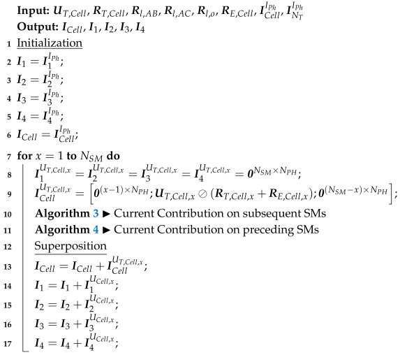
The consecutive execution of Algorithms 3 and 4 enables the determination of the current contributions of the voltage sources U T , C e l l , x for all cell and trace currents within the phase arms. The complete algorithm is presented in Algorithm 5. The individual voltage sources are processed sequentially in this study, using an additional outer iteration loop. In each iteration, the computed current contributions of the corresponding voltage source U T , C e l l , x are superimposed with the cell and trace currents determined in the previous iteration. The execution order of Algorithms 3 and 4 can be chosen arbitrarily.
The matrices I C e l l I P h and I N T I P h , determined by Equations (62)–(66), are used as initial conditions. After  N S M iterations, the current contributions of all current and voltage sources are superimposed, and the overall current distribution within the phase arms is determined by I 1 , I 2 , I 3 , I 4 , and  I C e l l . The superposition in each iteration also reduces memory usage. The overall algorithm presented in Algorithm 5 has a time complexity of O ( N S M 2 ) . This arises from the N S M iterations required to determine all current contributions of the voltage sources U T , C e l l , x using Algorithms 3 and 4. Furthermore, N S M iterations are required to compute the current contributions of all voltage sources within each phase arm. Due to the nesting of the iteration loops, the overall time complexity is the product of the individual loop’s complexities. In the case of parallel execution of the calculations for all voltage sources, the outer iteration loop can be omitted. While the total number of operations—and thus the time complexity—remains O ( N S M 2 ) , parallelization can reduce the wall-clock execution time by distributing these operations across multiple processing units.
Algorithm 5: Overall Current Distribution within PECIN Phase Arms
Batteries 12 00181 i005
The remaining currents I T U 1 and I T U 2 are determined by applying Kirchhoff’s current law, as given in Equations (68) and (69).
I T U 1 = I 1 , N S M I 3 , N S M I C e l l , N S M
I T U 2 = I 4 , N S M I 2 , N S M I C e l l , N S M

4.4. Temperature Distribution Within and Between PECIN SMs

Thermal interactions between the adjacent SMs in a phase arm are typical during inverter operation. The thermal behavior is also closely linked to the mechanical configuration of the PECIN MLI system. For functional benefits, SMs in a phase arm are often distributed across multiple modules.
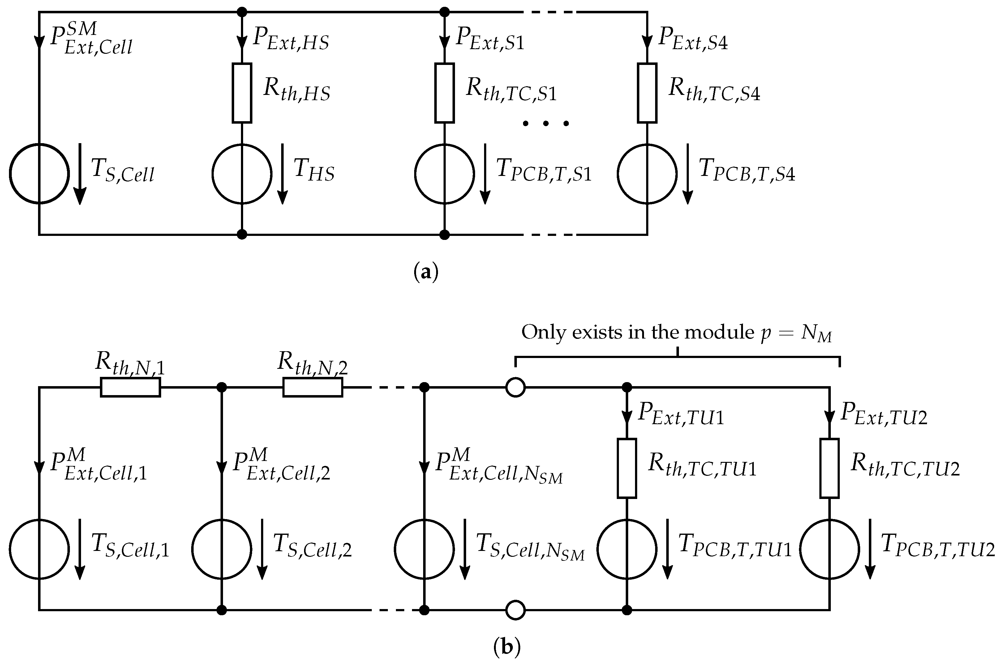
The employed temperature distribution model is an extension of the model proposed by Schmid et al. [21] for conventional battery systems and accounts for thermal coupling between battery cells in modules. The expanded thermal equivalent circuits shown in Figure 14 capture both the thermal coupling between different heat sources within an SM and the interactions between SMs.
The thermal coupling within an SM, depicted in Figure 14a, is represented by the thermal resistances R t h , T C , S x linking the individual PCB trace temperatures T P C B , T , S x to the cell surface temperature T C e l l , S . Additionally, the resistance R t h , H S accounts for the thermal connection to a cooling system, with the cooling medium temperature denoted as T H S . Variation of R t h , H S enables simplified analysis of system behavior under different thermal boundary conditions, with and without dedicated cooling. Natural or forced convection behavior is be approximated by assigning a large value (e.g., 10 20  KW−1) to R t h , H S , thereby effectively decoupling T H S . Under these conditions, heat can only be dissipated to the ambient via R t h , T A in Figure 5 and Figure 6.
Figure 14b shows the thermal circuit modeling interactions between SMs within the same module. Based on the thermal circuit, both module-to-pack and cell-to-pack systems concepts can be considered. The resistance R t h , N characterizes the thermal coupling between adjacent SMs within a module, whereas SMs in different modules are assumed to be thermally isolated. The SM adjacent to the Termination Unit also considers thermal coupling to the heat generation within the Termination Unit through the resistances R t h , T C , T U x , which link the PCB trace temperature potentials T P C B , T , T U x . The thermal coupling, based on the circuit in Figure 14a, is described using Kirchhoff’s voltage and current laws according to Equations (70)–(72).
P E x t , S x [ k ] = T S , C e l l [ k ] T P C B , T , S x [ k ] R t h , T C , S x
P E x t , H S [ k ] = T S , C e l l [ k ] T H S [ k ] R t h , H S
P E x t , C e l l S M [ k ] = P E x t , H S [ k ] P E x t , S 1 [ k ] P E x t , S 2 [ k ] P E x t , S 3 [ k ] P E x t , S 4 [ k ]
The heat flow P E x t , S x serves as the thermal coupling with the model in Section 3.4, capturing the temperature behavior of each PECIN copper trace along with the temperature dynamics of the single or BtB MOSFET. The coupling with the heat transfer rate P E x t , T U x of the Termination Unit is established in the same way and defined in Equation (73).
P E x t , T U x [ k ] = T S , C e l l , N S M [ k ] T P C B , T , T U x [ k ] R t h , T C , T U x
The surface temperature of the cell adjacent to the Termination Unit in each phase is denoted by T S , C e l l , N S M , where N S M also corresponds to the associated matrix row index. The thermal interactions between SMs can be evaluated collectively for all SMs in each phase using element-wise operations. Owing to the matrix-vector notation, Equations (76) and (77) are presented for each phase individually, indicated by the subscript j { 1 , 2 , , N P H } . The number of thermally coupled SMs within a module is given by N T C = N S M / N M , where N M denotes the number of modules per phase arm. Therefore, N M thermal networks, indexed by p { 1 , 2 , , N M } , can be set up for each phase arm, with each network being thermally isolated from the others. Furthermore, the auxiliary matrix W M is introduced.
W M = 1 1 0 0 0 1 1 0 0 0 1 1 R ( N T C 1 ) × N T C
Based on the Kronecker product between the unit matrix 𝟙 N M × N M and the auxiliary matrix W M , the block diagonal matrix W is defined.
W = 𝟙 N M × N M W M R ( N M · ( N T C 1 ) ) × N S M
The heat flow P N , j between adjacent SMs of a phase arm can be directly derived by rearranging the mesh equations, applying Kirchhoff’s voltage law.
P N , j = W · T S , C e l l , j R t h , N , j
Kirchhoff’s current law is applied to determine the heat flow for each cell P E x t , C e l l M . In this context, the unit vector e N S M = [ 0 , 0 , , 0 , 1 ] R N S M × 1 is introduced.
P E x t , C e l l , j M = W · P N , j e N S M · P E x t , T U 1 , j + P E x t , T U 2 , j
The resulting heat flow for each cell, obtained by superposition, represents the coupling with the thermal model outlined in Section 3.2.

P E x t , C e l l = P E x t , C e l l S M + P E x t , C e l l M

5. Simulation Results and Discussion

The complete simulation model was implemented in MATLAB/Simulink R2023b using forward Euler discretization of the system’s differential equations and the mathematical formulations presented in the preceding Sections. All simulations were performed using a fixed-step solver configuration with the Euler method (ode1) and executed on a standard laptop equipped with an Intel Core i7-8750H CPU (2.20 GHz), 16 GB of RAM, and a 512 GB solid-state drive, operating under Windows 11.
The model is parameterized based on an experimental PECIN MLI prototype. Parameters are derived from component characteristics (material, mass, dimensions), experimental measurements, and the scientific literature. To demonstrate the simulation framework’s capabilities, this work presents results from a grid-connected three-phase PECIN MLI during a grid start-up. This is followed by an analysis of the computational effort for individual model components to evaluate overall simulation performance. The model is subdivided into the following components: Electrical Battery Cell Model (EBM), Thermal Battery Cell Model (TBM), Electrical Trace Model (ETM), Thermal Trace Model (TTM), Thevenin Equivalent Transformation (TET), Electrical System Model (ESM), Current Distribution (CD), and Temperature Distribution (TD).

5.1. Model Parameterization

The simulation framework is parameterized according to a laboratory-scale demonstrator of the PECIN MLI, designed for use in a test bench focused on drive and grid applications. The central component of the demonstrator is the PCB, which implements the PECIN topology at the single-cell level. Referred to as the reference PCB in this study, the board includes the power path of an entire phase arm, consisting of 15 SMs, as well as the Closing and Termination Unit, and represents a refined version of the PCB used in previous studies [12,13]. The PCB was designed to minimize total phase resistance and optimized for high-current applications above 100 A , without requiring dedicated cooling for the MOSFET semiconductors.
The switching elements employed are low-voltage N-channel MOSFETs of type NVMTS0D4N04C from onsemi (Scottsdale, AZ, USA), characterized by a typical on-resistance of 380 μ Ω and a nominal drain-to-source breakdown voltage of 40 V [36]. Every single MOSFET within the PECIN topology is constructed from three discrete MOSFET semiconductor elements connected in parallel ( N F e t , P a r = 3 ). The same configuration applies to the BtB MOSFETs, which are each composed of six discrete MOSFET elements. The on-resistance for the single and BtB MOSFETs is thus approximately 127 μ Ω and 253 μ Ω ..
Each PECIN SM incorporates a lithium-ion battery cell of type UF261591 from Sanyo Panasonic (Osaka, Japan). This pre-production cell is designed for electric vehicle and plug-in hybrid electric vehicle applications, with a nominal voltage of 3.67   V and a nominal capacity of 25 A h . The battery cells employed in the PECIN MLI demonstrator originate from several distinct cell batches and have experienced substantial calendar aging. As a result, the capacity of the individual cells is diminished, and there is increased variation in capacity across cells. The electrical cell modeling parameters are partly derived from measurements conducted on the battery cells of the demonstrator and partly from [21], which reports extensive characterization measurements of this battery cell type.
A summary of the electrical and thermal parameters of the simulation framework, obtained from measurements and parameter calculations conducted in this study, is provided in Table 1 and Table 2. The copper resistances in the individual PECIN current paths were determined from the reference PCB design and validated by measurements. The additional system-level resistances and inductances of the ESM were also determined from test-bench measurements. The selected grid parameters were based on the assumption of strong grid conditions. For the model components EBM and ETM, a variation between the SMs was also considered, assuming that their parameters follow a normal distribution.
The thermal parameters in Table 2 were primarily determined by calculations based on the geometry and corresponding material properties, and subsequently validated using datasheet and additional literature data. A uniform distribution is applied to all thermal parameters, such that the TBM, TTM, and TD models employ identical parameters for every battery cell, PECIN path, and module.

5.2. Simulation Case Study of a Three-Phase Charging Operation
The following case study considers the laboratory-scale 31-level three-phase PECIN MLI, employed for model parameterization. The system configuration is defined by N P H = 3 , N S M = 15 , and N M = 1 . The simulation captures the initial phase of a three-phase charging operation on an AC supply with a voltage amplitude of 45 V and a frequency of 50 Hz , representing a downscaled grid.
For higher-level charge control, the PECIN MLI is controlled using a proportional-resonant controller in the α β stationary reference frame for current control, with space vector modulation [45] determining the output voltage levels and a switching function [13] mapping the reference levels to specific switching states of each switch. A three-phase locked loop tracks the grid angle to transform the current setpoint in the d q synchronous reference frame into the stationary frame. The modulation switching frequency also corresponds to the control update frequency and was set to 10 k Hz . Additionally, the control system includes a straightforward charge-balancing mechanism to equalize the SoC across cells in each phase arm. The balancing algorithm is triggered whenever the phase voltage crosses zero and prioritizes cells based on their SoC. The following simulations were performed with a time step of 1 μ s and a duration of either 150 m s or 1 s .
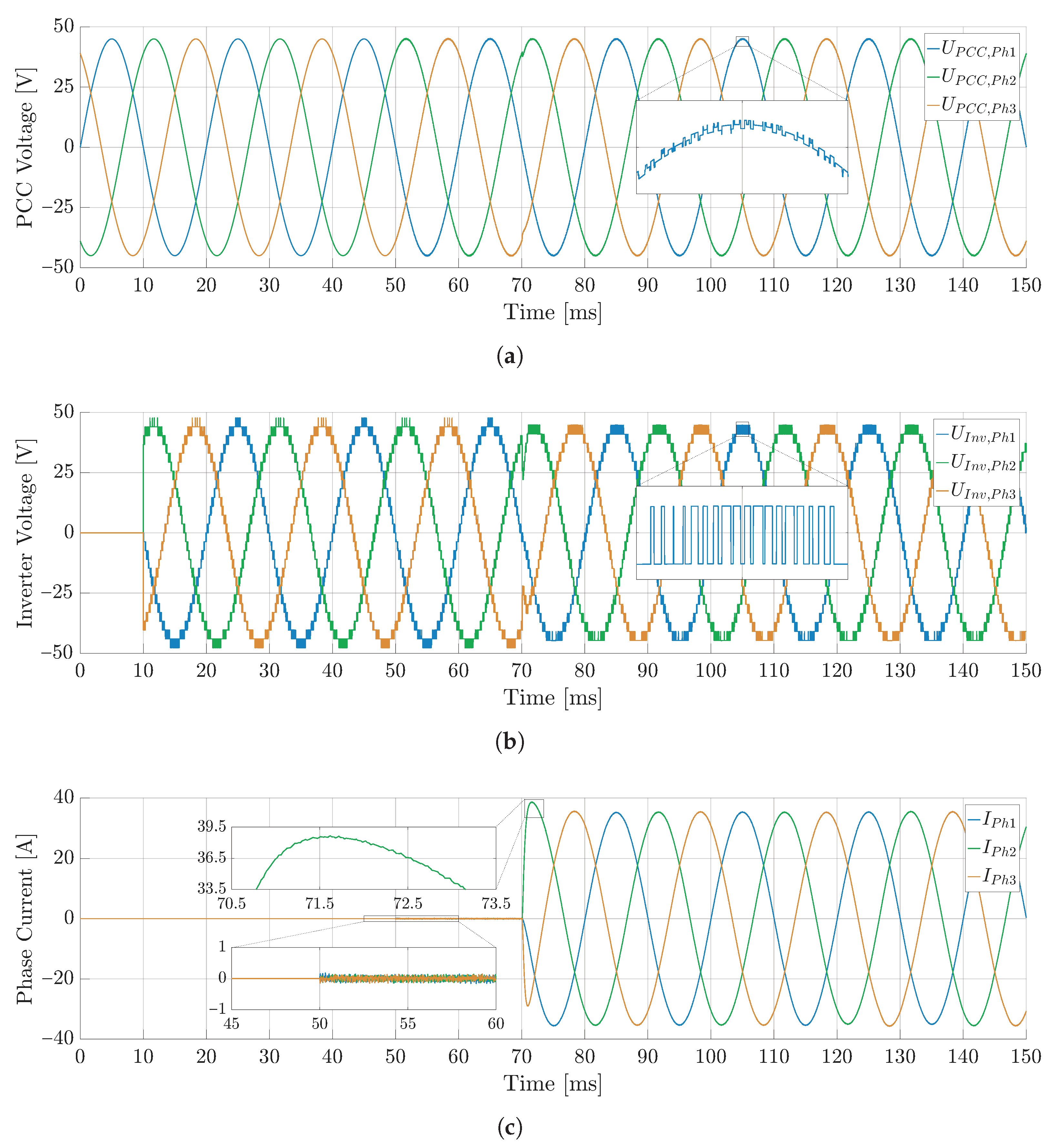
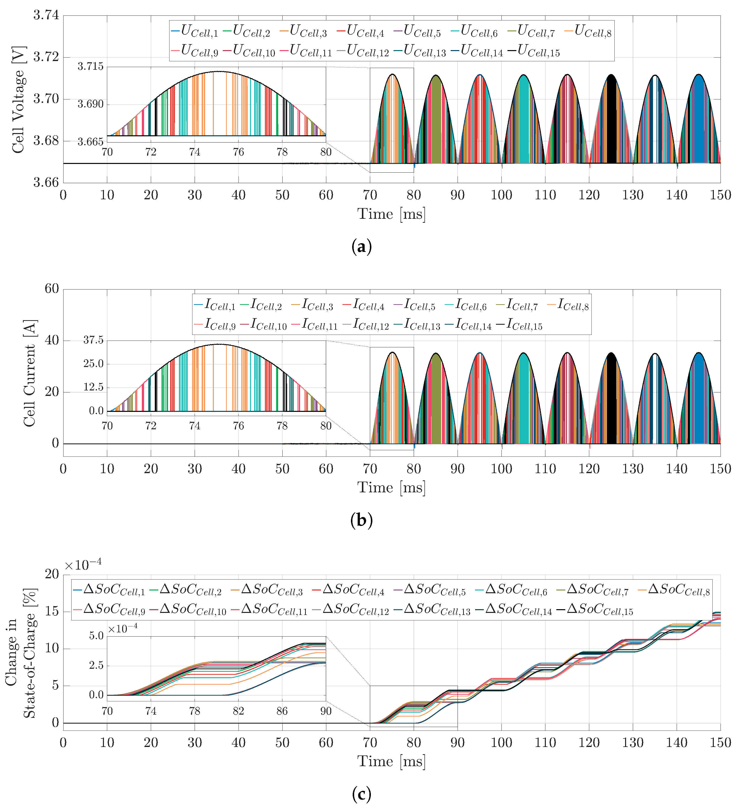
Figure 15 and Figure 16 show the simulated waveforms of the phase voltages and currents at the system level, as well as the evolution of cell voltages, currents, and SoCs for the phase arm of phase 1. The results demonstrate that the model can accurately resolve transient electrical behavior at both system and SM levels. For this simulation case, all battery cells are assumed to start with an initial SoC of 50%, corresponding to a normalized value of 0.5. The initial temperature conditions for the battery cell core and surface, as well as the single and BtB MOSFETs junction, case, and trace temperatures, were uniformly set to 25 °C. The PECIN MLI demonstrator is operated without a dedicated cooling system. Accordingly, the heat sink temperature T H S is decoupled from the system, and heat dissipation is limited to free convection to the ambient temperature T A set to 25 °C.
At the beginning of the simulation, between 0 s and 10 m s , all SMs of the PECIN MLI are configured in idle switching state, resulting in zero phase voltage in all three phases. The switches S P h , j that connect the inverter to the grid remain open, preventing a closed electrical circuit and resulting in zero phase current. At 10 m s , inverter operation is initiated, synchronizing the phase voltages with the grid voltage. The voltages U P C C measured at the PCC, averaged over each switching period, serve as input to the current-control. The switches S P h , j close at 50 m s , thereby establishing the electrical connection between the PECIN MLI and the grid. The phase currents indicate that the inverter phase voltages track the grid voltages closely in their average values, demonstrating proper closed-loop current control behavior. At 70 m s , the charging process is initiated by adjusting the current-control setpoint to a charging current of 25 A RMS (approx. 35.35   A Peak ).
The voltages and phase currents depicted in Figure 15 highlight the impact of the PECIN MLI switching operations, as captured by the switching-model approach. The inverter output voltages shown in Figure 15b reflect the characteristic multilevel switching behavior between discrete voltage levels, primarily governed by the space vector modulation. The resulting effects of these switching operations are also evident in the PCC voltages and phase currents depicted in Figure 15a,c.
The PCC voltages accurately reflect the electrical behavior of the adopted grid representation based on an ideal voltage source and a resistive–inductive grid impedance. During the interval from 0 s to 50 m s , no voltage drop occurs across the grid impedance, as the phase currents are zero. Consequently, the PCC voltage waveforms correspond to the assumed ideal sinusoidal grid voltages U G r i d . The zoomed-in section in Figure 15a at 105 m s provides an illustrative example of the impact of the switching operations of all three PECIN phase arms on U P C C , P h 1 . A similar behavior is observed in the zoomed-in sections in Figure 15c, where the phase currents exhibit a switching-induced ripple.
A harmonic analysis considering up to the 50th order indicates a harmonic distortion of approximately 4.7% for the inverter’s output phase voltages and about 0.7% for the phase currents in steady state. The phase shift between the fundamental grid voltages and phase currents is close to zero degrees, and the power factor is close to unity. This indicates purely active power transfer during the charging process.
The simulated cell voltages and currents provide insight into the impact of the switching operations on the clamping behavior of the battery cells. This behavior is described by the Dual-Polarization Thevenin Model, which constitutes the core of the EBM. The onset of the charging process at 70 m s is consistently reflected in all electrical quantities in Figure 16.
The cell currents I C e l l , obtained using the proposed current distribution algorithms, are either zero or equal to the phase current, reflecting that the PECIN MLI control in this simulation scenario is restricted to pure series reconfiguration. The cell voltages U C e l l reflect the electrical behavior at the cell terminals and are primarily governed, over the time interval shown, by the open-circuit voltage U O C V and the series resistance R 0 of the Dual-Polarization Thevenin Model. The influence of the two RC elements is negligible over this time interval due to their comparatively large time constants.
The gradual increase in the cell SoCs relative to the initial cell SoC at t = 0   s reflects the charging process and indicates the energy transfer from the grid to the battery cells. At the same time, the balancing mechanism limits deviations among individual cell SoCs. The prioritization of individual battery cells within the applied scheme is further reflected in the evolution of cell voltages, currents, and SoCs.
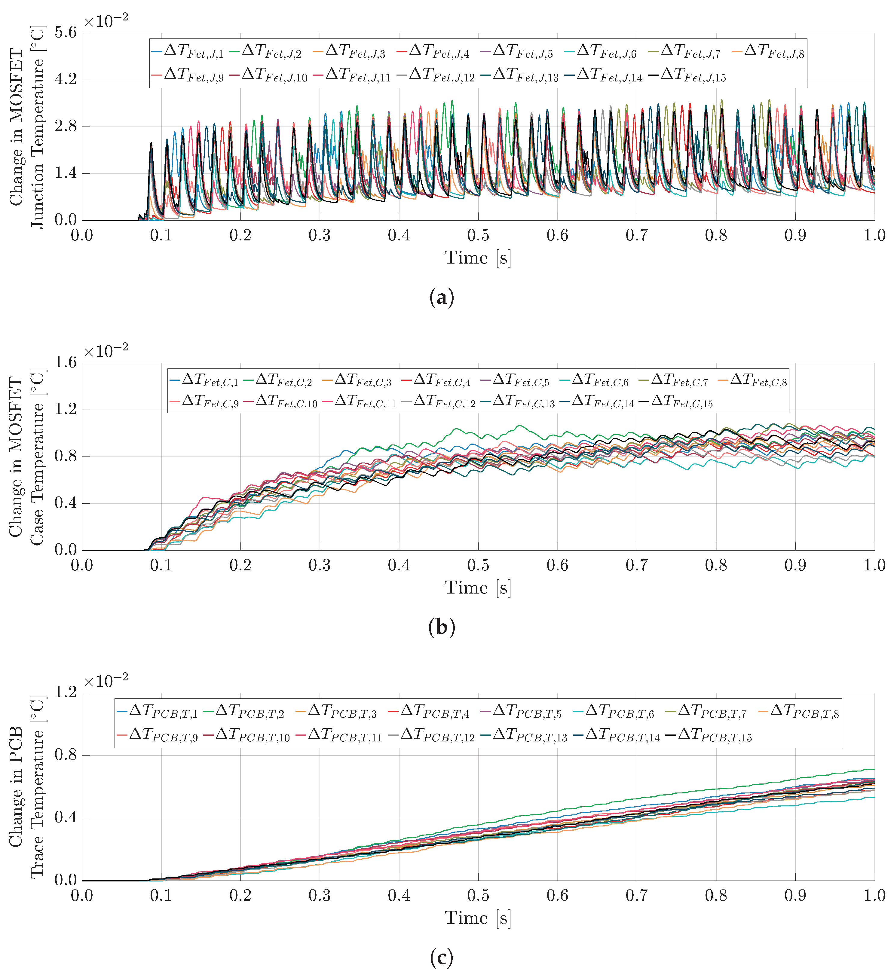
Following the analysis of the model’s capabilities in representing electrical system behavior, the thermal system dynamics are addressed. The analysis focuses on the dynamics included within the TTM, which captures MOSFET and PCB trace temperatures and exhibits different time constants. To observe the thermal dynamics, the simulation duration was extended to 1 s . The evolution of MOSFET and PCB trace temperatures associated with switch S 2 in the PECIN phase arm of phase 1 is illustrated in Figure 17. The temperature changes are shown relative to the initial temperature of 25 °C at time t = 0   s . The time constants associated with heat propagation in the MOSFET junction, case, and PCB trace are readily distinguishable. Each temperature increase corresponds to heat generation caused by the modeled conduction losses in the MOSFETs and PCB traces during the on-state of the respective switching element.

5.3. Execution Time Analysis

The execution time analysis within this study was conducted to quantify the computational efficiency of the model, identify the most computationally demanding components, and assess the impact of variations in the number of SMs on the execution time.
The evaluation was performed for the three-phase charging scenario of the grid-connected PECIN MLI. The Simulink Profiler was used to obtain the execution times and analyze the distribution among individual model components. For the analysis, the reference configuration used was the inverter model previously detailed, defined by the parameters N P H = 3 , N S M = 15 , and N M = 1 , with a simulation time step of 1 μ s . A simulation duration of 1 s was employed for all measurements. To remove the impact of graphical visualization on execution time, all graphs were removed after validating the simulated time traces.
To investigate the influence of the number of SMs N S M on execution time, the model was evaluated for 5, 10, 15, 25, and 50 SMs per phase arm. For each configuration with a given number of SMs, 10 simulation runs were performed to account for variations in execution time. Accordingly, the total number of SMs across all phases equals the product of N P H and N S M . A total of 106 simulation steps were executed in each run, which directly follows from the defined step size of 1 μ s and the total simulation time of 1 s .
The results, including mean values and standard deviations of execution times and relative time shares, with respect to the total execution time in each simulation run, are provided in Table 3 and Table 4. Execution times are reported for different model components, while the execution times of elements not assigned to any of these components (e.g., PECIN MLI control) are aggregated under the remaining part (REM). While absolute execution times are crucial for practical simulations, their dependence on hardware performance and the simulation tools limits their overall significance [14]. The relative shares of computational time provide a more generalizable perspective.
The execution times for EBM, TET, TBM, TTM, and TD, presented in Table 3, increase linearly with N S M , reflecting the O ( N S M ) computational complexity of these model components. In contrast, the execution time of the CD increases quadratically with N S M , as expected from its O ( N S M 2 ) algorithmic complexity. The dominant behavior of the CD with rising N S M is also evident from the relative time shares listed in Table 4. The execution time of the ESM remains nearly constant, with only a slight increase. This behavior stems from the fact that its complexity scales with N P H , rather than with N S M . Throughout the simulation, the model’s components are computed sequentially, resulting in an overall time complexity equal to the sum of the individual submodel complexities. The CD represents the dominant term and determines the overall model complexity as O ( N S M 2 ) . This quadratic scaling is also reflected in the total model execution times in Table 3.
The execution times obtained for the three-phase AC charging model configuration are largely transferable to the single-phase AC/DC charging configuration with the circuit topology depicted in Appendix A. The differences between the two model configurations are confined to the ESM, while the type, dimensionality, and number of operations remain identical across the remaining components. The matrix and vector operations of the ESM increase by one row and/or column due to the inclusion of an additional phase branch in the electrical circuit for single-phase AC/DC operation. As a result, the matrix-vector operations within the ESM require a slightly higher computational effort for the single-phase AC/DC charging operation compared to the three-phase AC charging configuration. Due to the minor contribution of the ESM to the overall execution time and the fact that N P H = 3 represents the typical case in most practical applications, a separate detailed analysis was omitted, as it has no significant impact on the overall computational effort.
The execution times of PECIN MLIs with up to 50 SMs per phase arm and simulation durations ranging from milliseconds to a few seconds remain low, enabling efficient evaluation. The model’s high level of detail, including the explicit representation of switching operations, further enables comprehensive analysis. This level of detail is particularly advantageous for evaluating low-level switching control algorithms, determining series and parallel reconfiguration of SMs, and analyzing dynamic system behavior within this time scale, as demonstrated in the simulation case study of a three-phase charging operation.
With increasing simulation duration, the number of required arithmetic operations and the model’s execution time scale approximately linearly. Consequently, simulations with durations of several minutes result in significant computational effort even for a moderate number of SMs. Such extended simulation horizons are required to capture electrical or thermal processes with time constants on the order of seconds to minutes, for example to evaluate SoC balancing mechanisms or cycle-based energy considerations.
For the reference PECIN MLI ( N P H = 3 , N S M = 15 , N M = 1 ), a 15 min simulation results in an execution time of approximately 1.9 days, based on the extrapolation of the measured execution times. This highlights a limitation arising from the frequent model evaluation by the fixed time-step size of 1 μ s for simulations at this time scale. Increasing the simulation time-step directly reduces the number of simulation steps and thus the computational effort. However, this approach imposes constraints on simulation accuracy, as it dictates the level of accuracy for the representation of switching events and affects numerical precision. The limitation is particularly restrictive when pulse width modulation techniques that rely on high-frequency switching operations are employed.
Potential approaches to address this limitation include assigning different time-step sizes to model components based on electrical and thermal time constants, applying adaptive time-step control triggered by switching actions, or parallelizing model components.

6. Conclusions and Outlook

This study presents a comprehensive simulation framework for symmetrical PECIN MLI with a single-cell architecture, enabling detailed analysis of electrical and thermal system behavior. The model further introduces novel iterative algorithms for the efficient computation of the electrical PECIN phase arm network.
The developed algorithms eliminate the need for high-dimensional matrix inversions, thereby reducing computational complexity and improving scalability with respect to the number of SMs. Execution time analysis further reveals that the calculation of the current distribution within phase arms remains the dominant contributor to the overall computational effort, thereby limiting the efficient simulation of large-scale PECIN MLIs. As this limitation is a consequence of the PECIN topology’s inherent parallel reconfiguration capabilities, it may also extend to other cascaded MLIs with equivalent functionality.
The proposed framework provides a scalable and efficient development platform for detailed studies of PECIN MLIs. The complete model and all required execution files are included in the Supplementary Material, enabling immediate application. It is well-suited for the development and evaluation of low-level switching control strategies, as well as for the analysis of transient processes on micro- and millisecond timescales.
The applicability of the model to extended simulation horizons remains computationally demanding due to the microsecond-scale time-step resolution required to accurately capture switching operations. This is inherent to the switching modeling approach adopted in this study. To address the applicability of the proposed framework for the analysis of full charging or discharging cycles, an average model will be derived from the switching model and presented in a subsequent publication. This will enable computationally efficient investigation of higher-level control strategies and system-level parameter studies beyond the switching time scale.

Supplementary Materials

The following supporting information can be downloaded at: https://www.mdpi.com/article/10.3390/batteries12050181/s1; PDF-File: Readme.pdf; MATLAB/Simulink-Files: CellData.mat; CustomNormRnd.m; Init_PECIN_SwitchingModel.m; PECIN_SwitchingModel.slx.

Author Contributions

Conceptualization, S.S. and C.T.; methodology, S.S.; software, S.S.; validation, S.S.; formal analysis, S.S.; investigation, S.S.; resources, S.S. and C.T.; data curation, S.S.; writing—original draft preparation, S.S.; writing—review and editing, C.T.; visualization, S.S.; supervision, C.E.; project administration, C.E.; funding acquisition, C.E. All authors have read and agreed to the published version of the manuscript.

Funding

We acknowledge support by the Open Access Publication Fund of Technische Hochschule Ingolstadt (THI).

Data Availability Statement

The original contributions presented in this study are included in the article/Supplementary Material. Further inquiries can be directed to the corresponding author.

Acknowledgments

The authors gratefully acknowledge Meinert Lewerenz for his valuable discussions and constructive suggestions regarding the presentation of the topic.

Conflicts of Interest

The authors declare no conflicts of interest.

Abbreviations

The following abbreviations are used in this manuscript:
BEVBattery Electric Vehicle
BtBBack-to-Back
CDCurrent Distribution
EBMElectrical Battery Cell Model
ESMElectrical System Model
ETMElectrical Trace Model
HVDCHigh-Voltage Direct-Current
MLIMultilevel Inverter
MOSFETMetal-Oxide-Semiconductor Field-Effect Transistor
PCBPrinted Circuit Board
PCCPoint of Common Coupling
PECINParallel Enhanced Commutation Integrated Nested
REMRemainder
SMSubmodule
SoCState-of-Charge
SPSwitching Pattern
TBMThermal Battery Cell Model
TDTemperature Distribution
TETThevenin Equivalent Transformation
TTMThermal Trace Model

Appendix A

Figure A1. Configuration of the electrical system circuit suitable for single-phase grid charging operation or DC charging operation with an external supply. With this setup, three PECIN phase arms are connected in parallel and connected to the grid or an external source. The passive circuit elements R G , 4 and L G , 4 represent an ohmic-inductive grid impedance with the grid voltage U G r i d , 4 or correspond to the ohmic-inductive impedance R E x t = R G , 4 and L E x t = L G , 4 of an external supply with U E x t = U G , 4 .
Batteries 12 00181 g0a1

References

  1. Gao, Z.; Xie, H.; Yang, X.; Zhang, L.; Yu, H.; Wang, W.; Liu, Y.; Xu, Y.; Ma, B.; Liu, X.; et al. Electric vehicle lifecycle carbon emission reduction: A review. Carbon Neutralization 2023, 2, 528–550. [Google Scholar] [CrossRef]
  2. Baumann, M.; Wildfeuer, L.; Rohr, S.; Lienkamp, M. Parameter variations within Li-Ion battery packs—Theoretical investigations and experimental quantification. J. Energy Storage 2018, 18, 295–307. [Google Scholar] [CrossRef]

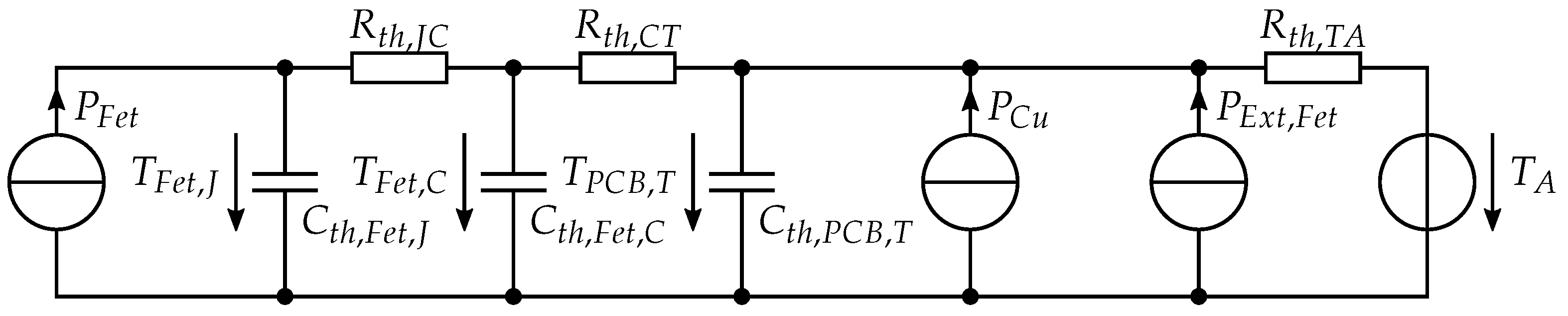
  3. Al-khdhairi, Y.M.S.; Vural, A.M. Study on the modeling and simulation of a grid-connected battery energy storage system based on cascaded h-bridge converter. Int. J. Energy Appl. Technol. 2021, 8, 98–112. [Google Scholar] [CrossRef]
  4. Chen, J.; Zhou, Z.; Zhou, Z.; Wang, X.; Liaw, B. Impact of battery cell imbalance on electric vehicle range. Green Energy Intell. Transp. 2022, 1, 100025. [Google Scholar] [CrossRef]
  5. Xu, Y.; Kersten, A.; Klacar, S.; Sedarsky, D. Maximizing Efficiency in Smart Adjustable DC Link Powertrains with IGBTs and SiC MOSFETs via Optimized DC-Link Voltage Control. Batteries 2023, 9, 302. [Google Scholar] [CrossRef]
  6. Leon, J.I.; Vazquez, S.; Franquelo, L.G. Multilevel Converters: Control and Modulation Techniques for Their Operation and Industrial Applications. Proc. IEEE 2017, 105, 2066–2081. [Google Scholar] [CrossRef]
  7. Korte, C.; Specht, E.; Hiller, M.; Goetz, S. Efficiency evaluation of MMSPC/CHB topologies for automotive applications. In Proceedings of the 2017 IEEE 12th International Conference on Power Electronics and Drive Systems (PEDS); IEEE: New York, NY, USA, 2017; pp. 324–330. [Google Scholar] [CrossRef]
  8. Stöttner, J.; Rauscher, A.; Endisch, C. Pareto optimization of multilevel inverter structures regarding the DC magnitude, switching frequency and switching angles. Int. J. Electr. Power Energy Syst. 2022, 142, 108259. [Google Scholar] [CrossRef]
  9. Poorfakhraei, A.; Narimani, M.; Emadi, A. A Review of Multilevel Inverter Topologies in Electric Vehicles: Current Status and Future Trends. IEEE Open J. Power Electron. 2021, 2, 155–170. [Google Scholar] [CrossRef]
  10. Ronanki, D.; Williamson, S.S. Modular Multilevel Converters for Transportation Electrification: Challenges and Opportunities. IEEE Trans. Transp. Electrif. 2018, 4, 399–407. [Google Scholar] [CrossRef]
  11. Komsiyska, L.; Buchberger, T.; Diehl, S.; Ehrensberger, M.; Hanzl, C.; Hartmann, C.; Hölzle, M.; Kleiner, J.; Lewerenz, M.; Liebhart, B.; et al. Critical Review of Intelligent Battery Systems: Challenges, Implementation, and Potential for Electric Vehicles. Energies 2021, 14, 5989. [Google Scholar] [CrossRef]
  12. Terbrack, C.; Stöttner, J.; Endisch, C. Design and Validation of the Parallel Enhanced Commutation Integrated Nested Multilevel Inverter Topology. IEEE Trans. Power Electron. 2022, 37, 15163–15174. [Google Scholar] [CrossRef]
  13. Terbrack, C.; Speer, S.; Endisch, C. Control and Implementation of the Parallel Enhanced Commutation Integrated Nested Multilevel Inverter Topology. Electronics 2023, 12, 3130. [Google Scholar] [CrossRef]
  14. Xu, J.; Zhao, C.; Liu, W.; Guo, C. Accelerated Model of Modular Multilevel Converters in PSCAD/EMTDC. IEEE Trans. Power Deliv. 2013, 28, 129–136. [Google Scholar] [CrossRef]
  15. Ahmed, N.; Ängquist, L.; Norrga, S.; Antonopoulos, A.; Harnefors, L.; Nee, H.P. A Computationally Efficient Continuous Model for the Modular Multilevel Converter. IEEE J. Emerg. Sel. Top. Power Electron. 2014, 2, 1139–1148. [Google Scholar] [CrossRef]
  16. Herath, N.; Filizadeh, S.; Toulabi, M.S. Modeling of a Modular Multilevel Converter With Embedded Energy Storage for Electromagnetic Transient Simulations. IEEE Trans. Energy Convers. 2019, 34, 2096–2105. [Google Scholar] [CrossRef]
  17. Parvari, R.; Filizadeh, S.; Fernando, I. Detailed Equivalent Modeling and Simulation of Modular Multilevel Converters with Partially- integrated Battery Energy Storage. J. Mod. Power Syst. Clean Energy 2024, 13, 1444–1457. [Google Scholar] [CrossRef]
  18. Gnanarathna, U.N.; Gole, A.M.; Jayasinghe, R.P. Efficient Modeling of Modular Multilevel HVDC Converters (MMC) on Electromagnetic Transient Simulation Programs. IEEE Trans. Power Deliv. 2011, 26, 316–324. [Google Scholar] [CrossRef]
  19. Peralta, J.; Saad, H.; Dennetiere, S.; Mahseredjian, J.; Nguefeu, S. Detailed and Averaged Models for a 401-Level MMC–HVDC System. IEEE Trans. Power Deliv. 2012, 27, 1501–1508. [Google Scholar] [CrossRef]
  20. Pereira, H.A.; Kontos, E.; Teodorescu, R. High level performance models of double-star MMC converters. In Proceedings of the 2017 IEEE 8th International Symposium on Power Electronics for Distributed Generation Systems (PEDG); IEEE: New York, NY, USA, 2017; pp. 1–6. [Google Scholar] [CrossRef]
  21. Schmid, M.; Vögele, U.; Endisch, C. A novel matrix-vector-based framework for modeling and simulation of electric vehicle battery packs. J. Energy Storage 2020, 32, 101736. [Google Scholar] [CrossRef]
  22. Cupertino, A.F.; Amorim, W.C.S.; Pereira, H.A.; Seleme Junior, S.I.; Chaudhary, S.K.; Teodorescu, R. High Performance Simulation Models for ES-STATCOM Based on Modular Multilevel Converters. IEEE Trans. Energy Convers. 2020, 35, 474–483. [Google Scholar] [CrossRef]
  23. Wen, L.; Hu, X.; Sun, Z.; Tang, S.; Hu, H.; Zhang, S. An Average Model for New Energy Generation Considering Period Losses and Locked State. In Proceedings of the 2024 3rd International Conference on Energy and Electrical Power Systems (ICEEPS); IEEE: New York, NY, USA, 2024; pp. 373–377. [Google Scholar] [CrossRef]
  24. Gupta, K.K.; Jain, S. Topology for multilevel inverters to attain maximum number of levels from given DC sources. IET Power Electron. 2012, 5, 435–446. [Google Scholar] [CrossRef]
  25. Theliander, O.; Kersten, A.; Kuder, M.; Han, W.; Grunditz, E.A.; Thiringer, T. Battery Modeling and Parameter Extraction for Drive Cycle Loss Evaluation of a Modular Battery System for Vehicles Based on a Cascaded H-Bridge Multilevel Inverter. IEEE Trans. Ind. Appl. 2020, 56, 6968–6977. [Google Scholar] [CrossRef]
  26. Yang, F.; Wang, D.; Zhao, Y.; Tsui, K.L.; Bae, S.J. A study of the relationship between coulombic efficiency and capacity degradation of commercial lithium-ion batteries. Energy 2018, 145, 486–495. [Google Scholar] [CrossRef]
  27. Lai, X.; Zhou, L.; Zhu, Z.; Zheng, Y.; Sun, T.; Shen, K. Experimental investigation on the characteristics of coulombic efficiency of lithium-ion batteries considering different influencing factors. Energy 2023, 274, 127408. [Google Scholar] [CrossRef]
  28. Cittanti, D.; Ferraris, A.; Airale, A.; Fiorot, S.; Scavuzzo, S.; Carello, M. Modeling Li-ion batteries for automotive application: A trade-off between accuracy and complexity. In Proceedings of the 2017 International Conference of Electrical and Electronic Technologies for Automotive; IEEE: New York, NY, USA, 2017; pp. 1–8. [Google Scholar] [CrossRef]
  29. Huria, T.; Ceraolo, M.; Gazzarri, J.; Jackey, R. High Fidelity Electrical Model with Thermal Dependence for Characterization and Simulation of High Power Lithium Battery Cells. In Proceedings of the 2012 IEEE International Electric Vehicle Conference; IEEE: New York, NY, USA, 2012; pp. 1–8. [Google Scholar] [CrossRef]
  30. Hu, X.; Li, S.; Peng, H. A comparative study of equivalent circuit models for Li-ion batteries. J. Power Sources 2012, 198, 359–367. [Google Scholar] [CrossRef]
  31. Saqli, K.; Bouchareb, H.; M’sirdi, N.K.; Oudghiri Bentaie, M. Lithium-ion Battery Electro-Thermal Modelling and Internal States Co-Estimation for Electric Vehicles. J. Energy Storage 2023, 63, 107072. [Google Scholar] [CrossRef]
  32. Mattia, L.; Beiranvand, H.; Zamboni, W.; Liserre, M. Lithium-ion battery thermal modelling and characterisation: A comprehensive review. J. Energy Storage 2025, 129, 117114. [Google Scholar] [CrossRef]
  33. Lin, X.; Perez, H.E.; Mohan, S.; Siegel, J.B.; Stefanopoulou, A.G.; Ding, Y.; Castanier, M.P. A lumped-parameter electro-thermal model for cylindrical batteries. J. Power Sources 2014, 257, 1–11. [Google Scholar] [CrossRef]
  34. Thomas, K.E.; Newman, J. Thermal Modeling of Porous Insertion Electrodes. J. Electrochem. Soc. 2003, 150, A176. [Google Scholar] [CrossRef]
  35. Kleiner, J.; Heider, A.; Komsiyska, L.; Elger, G.; Endisch, C. Thermal behavior of intelligent automotive lithium-ion batteries: Experimental study with switchable cells and reconfigurable modules. J. Energy Storage 2021, 44, 103274. [Google Scholar] [CrossRef]
  36. onsemi. Datasheet NVMTS0D4N04C: MOSFET—Power, Single N-Channel 40 V, 0.45 mOhm, 558 A, September 2021. Available online: https://www.onsemi.com/download/data-sheet/pdf/nvmts0d4n04c-d.pdf (accessed on 17 January 2026).
  37. Transmission & Distribution Committee of the IEEE Power and Energy Society. IEEE Recommended Practice and Requirements for Harmonic Control in Electric Power Systems; Institute of Electrical and Electronics Engineers: New York, NY, USA, 2014. [Google Scholar]
  38. Lahlou, T.; Abdelrahem, M.; Valdes, S.; Herzog, H.G. Filter design for grid-connected multilevel CHB inverter for battery energy storage systems. In Proceedings of the 2016 International Symposium on Power Electronics, Electrical Drives, Automation and Motion (SPEEDAM); IEEE: New York, NY, USA, 2016; pp. 831–836. [Google Scholar] [CrossRef]
  39. Buberger, J.; Hohenegger, M.; Estaller, J.; Wiedenmann, A.; Grupp, W.; Bliemetsrieder, W.; Kuder, M.; Lesnicar, A.; Weyh, T. Bidirectional Charging for BEVs with Reconfigurable Battery Systems via a Grid-Parallel Proportional-Resonant Controller. Electricity 2023, 4, 171–184. [Google Scholar] [CrossRef]
  40. Tresca, G.; Zanchetta, P. AC Direct Charging for Electric Vehicles via a Reconfigurable Cascaded Multilevel Converter. Energies 2024, 17, 2428. [Google Scholar] [CrossRef]
  41. Brand, M.J.; Berg, P.; Kolp, E.I.; Bach, T.; Schmidt, P.; Jossen, A. Detachable electrical connection of battery cells by press contacts. J. Energy Storage 2016, 8, 69–77. [Google Scholar] [CrossRef]
  42. Engelhardt, J.; Zepter, J.M.; Gabderakhmanova, T.; Marinelli, M. Efficiency Characteristic of a High-Power Reconfigurable Battery with Series-Connected Topology. In Proceedings of the 2022 International Power Electronics Conference (IPEC-Himeji 2022-ECCE Asia); IEEE: New York, NY, USA, 2022; pp. 2370–2376. [Google Scholar] [CrossRef]
  43. Schwertner, S.; Buchberger, T.; Diehl, S.; Ferg, R.; Hanzl, C.; Hartmann, C.; Hölzle, M.; Kleiner, J.; Komsiyska, L.; Lewerenz, M.; et al. Design and Implementation of an Intelligent Reconfigurable High-Voltage Battery System for Next-Generation Electric Vehicles. Batteries 2025, 11, 424. [Google Scholar] [CrossRef]
  44. Kuchling, H. Taschenbuch der Physik, 20th ed.; Fachbuchverlag Leipzig im Carl Hanser Verlag: Munich, Germany, 2011. [Google Scholar]
  45. Zhang, H.; Meng, Y.; Ning, L.; Zou, Y.; Wang, X.; Wang, X. Fast and simple space vector modulation method for multilevel converters. IET Power Electron. 2020, 13, 14–22. [Google Scholar] [CrossRef]
Figure 1. Overall structure of the proposed electro-thermal PECIN simulation framework.
Batteries 12 00181 g001
Figure 2. PECIN phase arm composed of N S M SMs and a Closing or Termination Unit at the ends of the phase arm. Each SM contains a single battery cell, two single MOSFETs, and two Back-to-Back (BtB) MOSFETs.
Batteries 12 00181 g002
Figure 3. Relevant SPs and their associated functional states of a PECIN SM.
Batteries 12 00181 g003
Figure 4. Electrical model of the PECIN current path within an SM incorporating the battery cell.
Batteries 12 00181 g004
Figure 5. Thermal model of the PECIN SM current path incorporating the battery cell.
Batteries 12 00181 g005
Figure 6. Thermal model of a switchable current path associated with the switches S 1 to S 4 within a PECIN SM and T U 1 and T U 2 of the Termination Unit, consisting of a single or BtB MOSFET and a PCB copper trace.
Batteries 12 00181 g006
Figure 7. Electrical model of a PECIN phase arm.
Batteries 12 00181 g007
Figure 8. Step-by-step transformation of the electrical network of a phase arm, with all voltage sources U T , C e l l treated as short circuits, for equivalent resistance calculation using Algorithm 1 (Closing Unit → Termination Unit).
Batteries 12 00181 g008
Figure 9. Step-by-step transformation of the electrical network of a phase arm, with all voltage sources U T , C e l l treated as short circuits, for equivalent resistance calculation using Algorithm 2 (Termination Unit → Closing Unit).
Batteries 12 00181 g009
Figure 10. Electrical equivalent circuit from the battery cell perspective of PECIN SMi within the phase arm j, where T1i,j and T2i,j denote the terminals of the circuit shown in Figure 4.
Batteries 12 00181 g010
Figure 11. Electrical circuit at the system-level for a three-phase PECIN MLI connected to the grid.
Batteries 12 00181 g011
Figure 12. Step-by-step reverse transformation of the phase arm’s electrical network toward the Termination Unit to determine the current contributions to the subsequent SMs, with the only voltage source U T , C e l l , i active and all other sources treated as short circuits, as applied in Algorithm 3.
Batteries 12 00181 g012
Figure 13. Step-by-step reverse transformation of the phase arm’s electrical network toward the Closing Unit to determine the current contributions to the preceding SMs, with the only voltage source U T , C e l l , i active and all other sources treated as short circuits, as applied in Algorithm 4.
Batteries 12 00181 g013
Figure 14. Thermal propagation model within and between SMs. (a) Network model of thermal interactions among SM components. (b) Network model of intra-module thermal interactions among SMs with p = N M = 1 .
Batteries 12 00181 g014
Figure 15. Simulated phase voltages and currents during start-up of three-phase grid charging: (a) phase voltages at the PCC, (b) PECIN MLI phase voltages, and (c) phase currents.
Batteries 12 00181 g015
Figure 16. Simulated electrical behavior of all battery cells in the PECIN phase arm of phase 1 during start-up of three-phase grid charging operation: (a) cell voltages, (b) cell currents, and (c) evolution of the cell SoCs relative to the initial values.
Batteries 12 00181 g016
Figure 17. Simulated temperature evolution of MOSFETs and PCB traces associated with PECIN switching elements S 2 within phase 1 during start-up of three-phase grid charging operation: (a) MOSFET junction temperatures, (b) MOSFET case temperatures, and (c) PCB trace temperatures.
Batteries 12 00181 g017
Table 1. Electrical properties of the model components EBM, ETM and ESM.
EBM Q C e l l [ Ah ] R C P [ μ Ω ] R C N [ μ Ω ] R C u , C e l l [ μ Ω ] R S h u n t [ μ Ω ]
21.84 ± 0.28 30 ± 1.0  1 30 ± 1.0  1 40 ± 0.4 60 ± 1.7
ETM R C u , S 1 , 0 [ μ Ω ] R C u , S 2 , 0 [ μ Ω ] R C u , S 3 , 0 [ μ Ω ] R C u , S 4 , 0 [ μ Ω ] R C u , T U , 0 [ μ Ω ]
10 ± 0.2 30 ± 0.6 30 ± 0.6 10 ± 0.2 8 ± 0.15
ESM R C I [ m Ω ] R C F [ m Ω ] R F [ m Ω ] R C G [ m Ω ] R G [ m Ω ]
2.02.52.55.51.0
L C I [ μ H ] L C F [ μ H ] L F [ μ H ] L C G [ μ H ] L G [ μ H ]
5.05.01304030
1 Mean and standard deviation according to measurement data from [2,41,42,43].
Table 2. Thermal properties of the model components TBM, TTM and TD.
General T A [°C] T H S [°C] T C u , 0 [°C] α C u [ K 1 ]
252020 10.0039 1
TBM R t h , C S [ K W 1 ] R t h , S T [ K W 1 ] R t h , T A [ K W 1 ]
1.773 20.7525
C t h , C e l l , C [ J K 1 ] C t h , C e l l , S [ J K 1 ] C t h , C e l l , T [ J K 1 ]
556 21139
TTM R t h , J C [ K W 1 ] R t h , C T [ K W 1 ] R t h , T A [ K W 1 ]
0.61 30.6525
C t h , F e t , J [ J K 1 ] C t h , F e t , C [ J K 1 ] C t h , P C B , T [ J K 1 ]
0.00670.282.2
TD R t h , H S [ K W 1 ] R t h , T C [ K W 1 ] R t h , N [ K W 1 ]
0.753.420.51
1 Reference temperature and temperature coefficient of copper according to [44]. 2 Values adopted from the thermal parameter calculations of Schmid et al. [21]. 3 Data from the MOSFET datasheet for the NVMTS0D4N04C [36].
Table 3. Mean and standard deviation of model component execution times for different numbers of SMs per phase arm N S M , obtained with a simulation step size of 1 μ s and duration of 1 s .
Number of SMs per PECIN Phase Arm N SM
5 10 15 25 50
EBM9.75 ± 0.33 s14.70 ± 0.24 s19.82 ± 0.34 s29.23 ± 0.75 s54.87 ± 1.05 s
TET3.22 ± 0.07 s5.45 ± 0.12 s7.90 ± 0.10 s12.46 ± 0.19 s24.20 ± 0.32 s
ESM2.59 ± 0.07 s2.61 ± 0.06 s2.89 ± 0.05 s2.89 ± 0.09 s3.68 ± 0.16 s
CD7.79 ± 0.25 s21.51 ± 0.36 s46.68 ± 0.69 s134.23 ± 1.95 s502.77 ± 8.61 s
TBM6.51 ± 0.23 s9.47 ± 0.18 s12.55 ± 0.23 s18.31 ± 0.44 s33.85 ± 0.73 s
TTM7.39 ± 0.41 s12.02 ± 0.23 s16.75 ± 0.25 s25.85 ± 0.58 s49.96 ± 1.09 s
TD1.38 ± 0.07 s1.92 ± 0.06 s2.54 ± 0.06 s3.65 ± 0.11 s6.51 ± 0.10 s
REM41.23 ± 1.34 s47.18 ± 0.92 s72.67 ± 1.46 s77.88 ± 2.57 s155.04 ± 2.73 s
Total79.86 ± 2.72 s114.86 ± 1.75 s181.80 ± 2.84 s304.50 ± 6.25 s830.88 ± 12.58 s
Table 4. Mean and standard deviation of model execution time shares per simulation run, expressed relative to total execution time, for varying numbers of SMs per phase arm N S M .
Number of SMs per PECIN Phase Arm N SM
5 10 15 25 50
EBM12.2 ± 0.07%12.8 ± 0.12%10.9 ± 0.07%9.6 ± 0.08%6.6 ± 0.03%
TET4.0 ± 0.06%4.7 ± 0.07%4.3 ± 0.02%4.1 ± 0.03%2.9 ± 0.01%
ESM3.2 ± 0.04%2.3 ± 0.03%1.6 ± 0.02%0.9 ± 0.02%0.4 ± 0.02%
CD9.8 ± 0.06%18.7 ± 0.18%25.7 ± 0.20%44.1 ± 0.33%60.5 ± 0.31%
TBM8.2 ± 0.07%8.2 ± 0.07%6.9 ± 0.06%6.0 ± 0.05%4.1 ± 0.03%
TTM9.3 ± 0.21%10.5 ± 0.11%9.2 ± 0.06%8.5 ± 0.07%6.0 ± 0.05%
TD1.7 ± 0.04%1.7 ± 0.03%1.4 ± 0.02%1.2 ± 0.02%0.8 ± 0.01%
REM51.6 ± 0.18%41.1 ± 0.51%40.0 ± 0.35%25.6 ± 0.42%18.7 ± 0.33%
Total100.0 ± 0.00%100.0 ± 0.00%100.0 ± 0.00%100.0 ± 0.00%100.0 ± 0.00%
Disclaimer/Publisher’s Note: The statements, opinions and data contained in all publications are solely those of the individual author(s) and contributor(s) and not of MDPI and/or the editor(s). MDPI and/or the editor(s) disclaim responsibility for any injury to people or property resulting from any ideas, methods, instructions or products referred to in the content.