Article

Impacts of Curing-Induced Phase Segregation in Silicon Nanoparticle-Based Electrodes

by
Zoey Huey
1,2,
G. Michael Carroll
1,
Jaclyn Coyle
1,
Patrick Walker
1,
Nathan R. Neale
1,
Steven DeCaluwe
2 and
Chunsheng Jiang
1,*
1
Materials, Chemical, and Computational Science Directorate, National Renewable Energy Laboratory, 15013 Denver West Parkway, Golden, CO 80401, USA
2
Colorado School of Mines, Department of Mechanical Engineering, 1500 Illinois Street, Golden, CO 80401, USA
*
Author to whom correspondence should be addressed.
Batteries 2024, 10(9), 313; https://doi.org/10.3390/batteries10090313
Submission received: 5 July 2024 / Revised: 29 August 2024 / Accepted: 30 August 2024 / Published: 3 September 2024

Abstract

:
We report the investigation of silicon nanoparticle composite anodes for Li-ion batteries, using a combination of two nm-scale atomic force microscopy-based techniques: scanning spreading resistance microscopy for electrical conduction mapping and contact resonance and force volume for elastic modulus mapping, along with scanning electron microscopy-based energy dispersion spectroscopy, nanoindentation, and electrochemical analysis. Thermally curing the composite anode—made of polyethylene oxide-treated Si nanoparticles, carbon black, and polyimide binder—reportedly improves the anode electrochemical performance significantly. This work demonstrates phase segregation resulting from thermal curing, where alternating bands of carbon and silicon active material are observed. This electrode morphology is retained after extensive cycling, where the electrical conduction of the carbon-rich bands remains relatively unchanged, but the mechanical modulus of the bands decreases distinctly. These electrical and mechanical factors may contribute to performance improvement, with carbon bands serving as a mechanical buffer for Si deformation and providing electrical conduction pathways. This work motivates future efforts to engineer similar morphologies for mitigating capacity loss in silicon electrodes.

1. Introduction

Demand for electric vehicles with longer driving ranges has spurred increased need for lighter lithium-ion batteries (LIBs) [1]. Silicon (Si) is a promising anode material for this purpose, as it has a much higher theoretical capacity (3579 mAh gSi−1) than the current commercial graphite anode (Gr, 372 mAh gGr−1) [2,3]. However, Si undergoes a large volumetric change during lithiation, which has limited its widespread implementation [3]. The expansion and contraction that occur during cycling results in mechanical failure and disrupts the solid-electrolyte interphase (SEI). A stable and passivating SEI is crucial for long cycle life, as it protects the Si from parasitic reactions and capacity fade [4,5,6]. Current industrial silicon electrodes typically only achieve 80% capacity retention over several hundred cycles and have useful cycle lifetimes of approximately 100 cycles, which is significantly below what is currently achieved with graphite-only anodes [7].
Si nanoparticles (NPs) present a possible avenue for improved anodes because the increased surface-to-volume ratios allow for quicker lithiation and delithiation and decreased damage due to volumetric expansion [8]. One NP fabrication method is plasma-enhanced chemical vapor deposition (PECVD) using silane (SiH4) gas, which produces hydrogen-terminated silicon NPs [9]. These NPs do not disperse when mixed in a polar solvent, such as N-methyl pyrrolidone (NMP), which results in electrodes printed from NMP slurries exhibiting non-optimal particle distribution and poor electron percolation of electron-conducting phases [7,10]. To prevent this, the Si NPs can be coated with hydrophilic molecules, such as polyethylene oxide (PEO), which renders the particles dispersible in NMP. To remove the PEO coating, which inhibits electronic conduction and enables Si NP aggregation during cycling, thermal curing is conducted after electrode fabrication [7,11].
It has been demonstrated that this thermal curing greatly improves silicon utilization and first-cycle losses in thin electrodes [7]. However, as areal capacity increases with thickness, silicon utilization decreases in thermally cured electrodes [7]. In this work, we seek to understand the morphology as well as electrical and mechanical properties of thermally cured electrodes so that strategies can be developed for how to maintain high performance at greater thicknesses.
Scanning probe microscopy (SPM) is a powerful tool for characterizing battery samples due to its nanoscale resolution and wide array of measurement modes, including the widely used atomic force microscopy (AFM) [12]. Several SPM modes of interest to this field are scanning spreading resistance microscopy (SSRM) and contact resonance force microscopy (CRFM). SSRM measures localized electronic resistivity in a wide range of materials, from insulators to semiconductors to conductors, and is helpful in imaging different components in composite electrodes [13]. CRFM measures nanoscale mechanical properties to inform electrode engineering efforts to mitigate mechanical failure due to Si expansion.
SSRM is a two-terminal resistance measurement technique. A bias voltage is applied between the probe and the sample, and the sum of series resistances along the current path is measured. Because the electrical current spreads rapidly as it moves away from the probe/sample contact, the spreading resistance is dominated by the local resistivity of the sample right beneath the probe in ~50 nm hemisphere volumes. SSRM has a variety of applications in battery research, such as studying SEI resistivity [14,15,16], material degradation after cycling [17], and component visualization [13].
Contact resonance and force volume (CR-FV) are two nm-scale mechanical characterization methods based on AFM that measure modulus, along with other mechanical properties [18,19]. Each is suited to materials with different modulus and hardness ranges, allowing for the measurement of varied components in multiphase electrodes where mechanical properties can span a wide value range. To comprehensively understand the mechanical properties of composite electrodes, this work combines these two techniques, performed simultaneously, to provide a semi-quantitative mapping of mechanical properties and component distribution heterogeneity.
Here, we report a novel application of SSRM and CR-FV characterization for phase identification and measurement in battery electrodes, along with scanning electron microscopy-energy dispersive spectroscopy (SEM-EDS) and instrumental nanoindentation on composite anodes with PEO-treated Si NPs, conductive carbon, and binder. The anode shows phase segregation after thermal curing. Further, these distinct carbon-rich and Si-rich domains remain during cycling but have notably different resistivities and largely different mechanical properties from the pristine anode. Potential mechanisms for electrode cycling performance improvement through improved electronic pathways and mechanical strain relief due to phase segregation will be discussed.

2. Results

To understand the influence of thermal curing on electrode properties and morphology, this paper presents the electrical, mechanical, and chemical characterization of electrodes before and after the curing step in their pristine state, as well as after cycling.

2.1. Pristine Electrodes

2.1.1. Phase Morphology and Identification

Comparison of uncured and cured pristine (i.e., before cycling) PEO-coated Si (Si@PEO) electrode cross sections, as shown in Figure 1, reveals a significant change in the component distribution by curing. SEM-EDS imaging of the uncured electrode shows a relatively homogeneous distribution of carbon (C45 carbon black) and Si (Si@PEO active Si NPs) throughout the electrode (Figure 1a). The cured electrode, meanwhile, has smaller “band”-like domains that show more carbon signal than the surrounding areas. These surrounding areas show a higher Si concentration than the band structures, indicating that the carbon and Si separate from each other during curing. Note that the EDS interaction depth (µm) is significantly larger than the carbon (~100 nm) and Si particle sizes (<10 nm), so the maps represent data from several microns in the depth direction and show that the visible band structures exist three-dimensionally in the electrode [20].
Due to the intrinsic and contrasting electronic properties of the carbon and Si components, this phase segregation impacts the electrode’s physical properties. SSRM maps of the local electrode resistivity (Figure 1b) also reveal morphology change during curing consistent with the SEM-EDS data but with better resolution due to the intrinsic resolution difference of both the tools and the shallow SSRM detection depth (~50 nm). In the uncured electrode, the lower resistivity carbon particles are visible in a surrounding higher resistivity matrix and are distributed relatively uniformly through the electrode thickness. The surrounding matrix contains Si particles (identified in EDS) and appears as a high resistivity area rather than as discrete particles, due in part to the particle size being smaller than the SSRM resolution and to the high resistivity binder surrounding the Si NPs. The cured electrode shows lower resistivity bands, corresponding to the carbon particles. The local resistivity values measured in the carbon-rich and Si-rich domains of both electrodes were compared and no significant change during curing was found (Figure 1c). This similarity indicates that there is no change in the materials themselves during curing. The average overall resistivity for the cured sample is higher than that of the uncured sample (Figure 1c), likely due to the lower-resistivity carbon particles moving closer together and covering less area of the two-dimensional SSRM maps. However, the three-dimensional electrical conduction pathway is a direct factor affecting the electrode performance rather than the two-dimensional averaged resistivity. The carbon band structure in the cured sample provides an effective conduction network rather than the distributed carbon particles in the uncured electrode. Resistivity maps for thinner cured electrodes (1 µm and 6 µm) show similar carbon bands present (Figure S1). As a final check for the carbon-rich and Si-rich phase identifications, the area fractions of each domain measured based on resistivity match well with the calculated volume fraction of each component based on the compositions (Table S1), further demonstrating no significant intrinsic material changes during curing.

2.1.2. Mechanical Properties

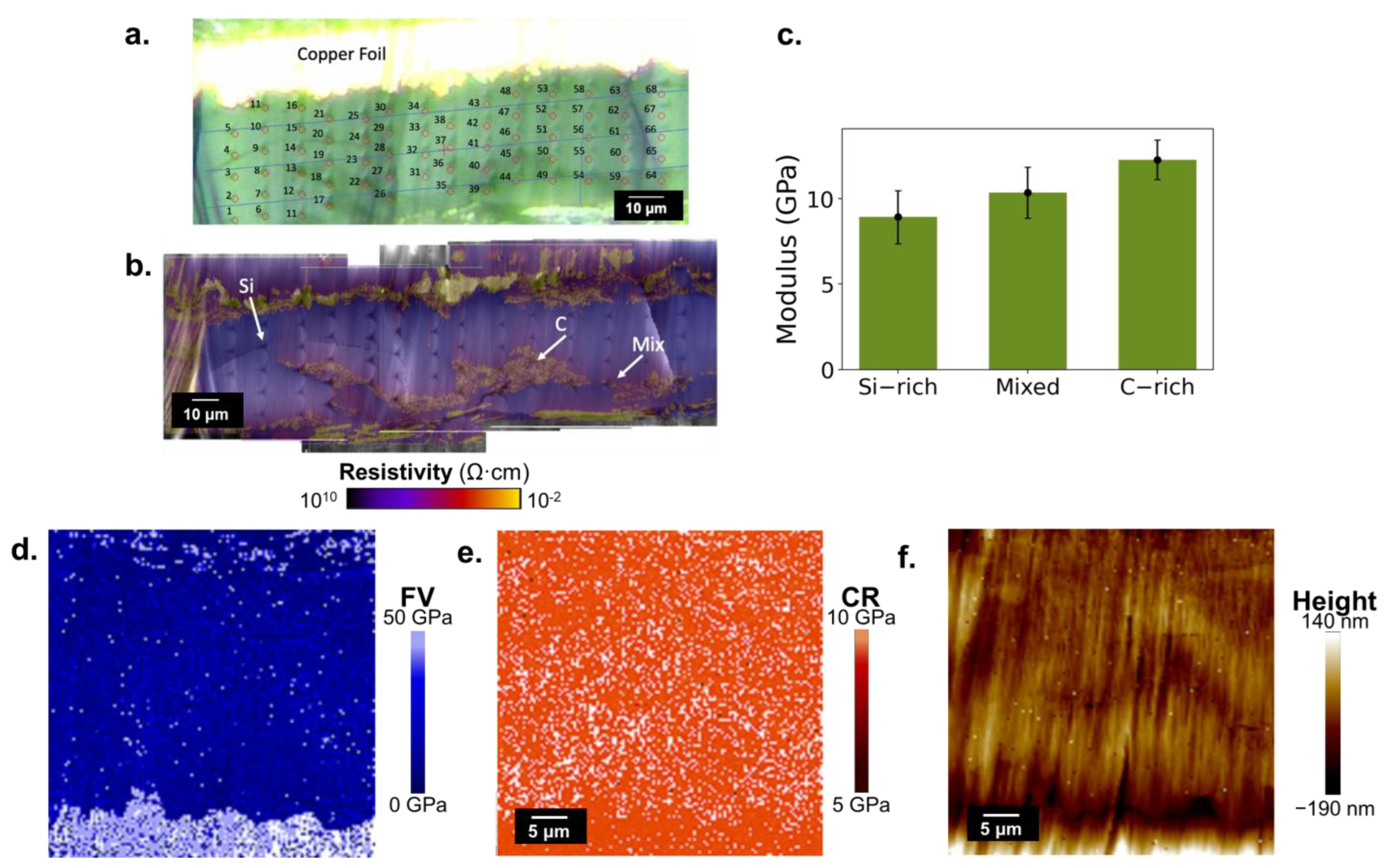
Nanoindentation was used to quantify the mechanical properties of the phase-segregated electrodes (Figure 2a). After the nanoindentation data were collected, the sample was imaged in the same area with SSRM (Figure 2b). By overlaying the corresponding AFM height and SSRM resistivity maps, the phase associated with each indent was determined based on the corresponding resistivity. The Si-rich domains showed a slightly lower modulus than the carbon-rich domains (Figure 2b), while the mixed domains have an intermediate modulus. Both CR and FV maps of the pristine cured electrode (Figure 2c) show homogeneous mechanical properties through the electrode thickness. The main advantage of AFM-based CR-FV is the nm-scale spatial resolution that is necessary for characterizing the Si NP composite anode, as demonstrated in later sections on cycled electrodes. However, the technique lacks the sensitivity for measuring the absolute elastic modulus values, such as the slight difference between domains in the pristine electrode, as shown by the nanoindentation. CR-FV data of the pristine uncured electrode was also collected (Figure S2); a similarly low uniform modulus was observed with no distinguishable morphological features.

2.2. Cycled Electrodes

2.2.1. Cycled Uncured Electrodes

An uncured sample was measured with SSRM and CR-FV after 25 cycles to investigate property changes after cycling. The SSRM map showed a slight overall increase in resistivity, with lower resistivity areas distributed evenly through thickness, consistent with the uniform carbon distribution in the uncured pristine sample (Figure 3a). It should be noted that the SSRM maps of cycled samples are typically lower quality compared to pristine due to SEI formation, which can be scraped off the sample by the probe tip, become adhered to the probe, and cause streak artifacts. The CR-FV maps (Figure 3c,d) show more heterogeneity as compared to this pristine electrode (a greater range in modulus) throughout the electrode thickness, although there are no distinct domains observed. The average modulus is higher than in the pristine electrode.

2.2.2. Cycled Cured Electrodes

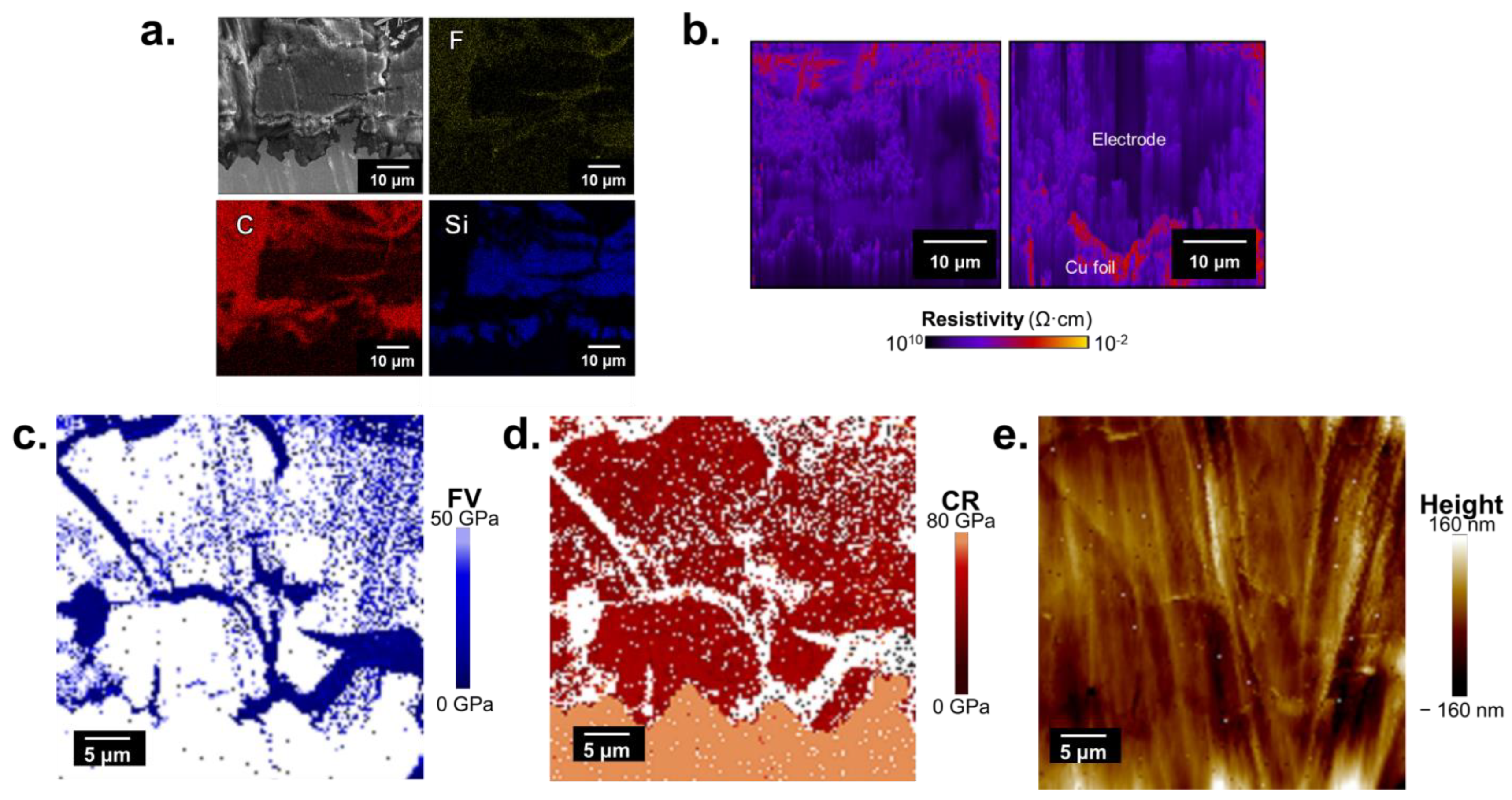
We characterized a cured electrode after 25 cycles to determine if the carbon-Si segregation was preserved during cycling and if it impacted other properties. EDS maps of the cycled cured electrode show similar carbon bands and surrounding areas of Si (Figure 4a). Additionally, SEM images show a crack-like morphology corresponding to the carbon-rich areas. There is some carbon present in the Si-rich areas; this is expected, as the SEI consists of various organic species originating from the electrolyte [4,21]. Fluorine, which is sourced only from the electrolyte, appears more concentrated in carbon-rich regions, indicating that SEI is preferentially formed in the region that is along the electrical current routes.
Resistivity maps of the same electrode (Figure 4b) show a slight overall increase in resistivity, which is expected in cycled electrodes due to the resistive SEI formation and material degradation, particularly of Si, during cycling, and the resistivity increase has been observed in other types of Si electrodes measured with SSRM [14,16,17]. While SSRM is a nm-scale mapping technique for local electronic resistivity of the electrode, electrochemical impedance spectroscopy (EIS) that is widely used in battery area is a macroscopic measurement and is dominated primarily by ion transport in a cell. EIS previously conducted on the same type of electrodes in symmetric cells showed an overall decrease in impedance after curing [7], but the results are not appropriate to compare directly with SSRM due to the fundamental differences of the techniques. Similar to the pristine cured sample, we observed low-resistivity carbon-rich bands in the cycled cured electrode. Like the cycled uncured electrode, the streak features in the SSRM scanning direction are caused by the adhesion of SEI materials to the probe during scanning.
CR-FV maps show that the mechanical properties changed significantly during cycling (Figure 4c,d). CR, best suited for higher modulus materials, shows an “island”-like morphology of high-modulus material, surrounded by areas where CR data could not be collected. FV, best for lower modulus materials, shows nearly the inverse of CR, with bands of material only measured with FV. Because of the complementary measurement ranges of these two techniques, we can conclude that the “islands” have a much higher modulus than the surrounding “bands”. The CR-FV map morphology closely matches the carbon- (bands) and Si-rich (islands) areas seen in the EDS and SSRM maps of this sample.

3. Discussion

3.1. Carbon and Silicon Phase Segregation

SEM-EDS and SSRM imaging of pristine electrodes showed the formation of a distinct band-like morphology, where the carbon separated from the Si during thermal curing (Figure 1). Similar imaging of a cured electrode after 25 cycles (Figure 4), as well as CR-FV mechanical maps, showed that this morphology was preserved during cycling, resulting in non-uniform electrical and mechanical properties.
One possible mechanism for the phase morphology evolution during curing is via binder flow during heating and the preferential adsorption of P84 binder to the C45 over the Si. Burdette-Trofimov et al., in a study with the same binder and conductive carbon along with milled Si, found that C45 could adsorb P84 binder up to 9.5 wt% in solution [22]. The Si could only adsorb 0.5 wt% of the binder. Because the binder preferentially adsorbs to the C45, it may be moved by the binder during curing while the Si is left behind, resulting in the phase segregation observed. However, more study is required to identify the exact mechanism that results in this morphology and what variables can be modified to adjust and refine it.

3.2. Contact Resonance-Force Volume for Composite Electrodes

Quantitative CR-FV data are reliant on proper calibration based on a known reference sample, the spring constant of the probe cantilever used in relation to the sample modulus, and a known probe-sample contact area [23,24]. These requirements are challenging to meet in a composite electrode system, so the absolute modulus values from CR-FV measurements presented here should be considered qualitative. However, there is still utility for CR-FV use in composite electrodes for the comparison of mechanical data across a sample set and in the spatial mapping of sub-micron features within an image.
Nanoparticle composites exhibit complex mechanical behaviors and can be impacted by multiple factors, including the mechanical properties of the particle material, particle size and loading, interfacial chemistry between the particles and the polymer binder, and properties of the polymer matrix itself. Additionally, reported SEI moduli vary significantly, ranging from 100 s of MPa to over 50 GPa [25,26,27]. All these factors make it difficult to predict the electrode material modulus [28,29]. Thus, a wide range of moduli may be present in nanocomposite electrodes. The modulus range for which FV is most accurate is dictated by the probe stiffness used to measure, while CR is somewhat less reliant on probe stiffness but generally requires a stiff probe to measure resonant oscillation frequency [23,30,31]. To accommodate the wide potential modulus range and for consistency across the sample set, the same probe type with a relatively high stiffness (Bruker DDLTESP, nominal k = 95 N/m) was used for all measurements, which means that the moduli measured in the cycled electrodes by CR is more accurate than as measured by FV.
Sample smoothness is also a challenge when measuring composite electrodes, as they are inherently rough [16]. These electrodes were cross-sectionally polished with an Ar-ion polisher, which improves sample smoothness compared to a surface measurement, but due to porosity and small variations in polishing rates of the different materials, some roughness (on the order of standard height deviation (Rq) of 20–100 nm) is unavoidable. CR modulus measurements are calculated using probe-sample contact area, which is calculated indirectly from known sample calibration. Increased roughness means less consistency in the contact area, introducing a source of error [30,31,32].
An example of the CR-FV sensitivity/accuracy is seen when comparing the nanoindentation and CR-FV data from the pristine cured electrode. The nanoindentation data, taken on a pristine cured electrode, showed a small but measurable difference in the modulus of the two phases, measuring 12.3 GPa as the carbon-rich average modulus and 8.9 GPa as the Si-rich modulus (Figure 2a,b). The CR-FV maps for the same sample, however, showed no distinguishable domains, with an FV average of 11.2 GPa and a CR average of 8.5 GPa. (Figure 2c,d, Table 1), suggesting that the 3.4 GPa difference observed with nanoindentation is below the accuracy limits of CR-FV for this sample. These values are likely influenced by the polymer binder used, which has a reported modulus of 3–4 GPa [33,34].
CR-FV mapping of the cycled samples provides useful information that cannot be obtained with nanoindentation, as the resolution that is necessary for identifying domains in 1 μm or less is challenging to measure by nanoindentation, which has a large measurement depth. The uncured cycled sample had an average FV modulus of 73.3 GPa and a CR modulus of 41 GPa, a large increase from the pristine samples. The FV modulus with this probe stiffness is less reliable at modulus ranges higher than approximately 10 GPa, which is likely why the FV value is measured significantly higher than reported SEI modulus estimates and higher than the CR value [35,36]. While CR-FV measurements are surface sensitive, on the order of 100 nm, the exact depth sensitivity is dependent on a number of variables, including probe flexural mode and mechanical properties, contact force applied, and probe-surface contact area. Since not all these are easily controllable for these samples, the precise measurement depth cannot be estimated accurately [37]. The SEI can range from several to several 10s of nanometers in thickness as well and has a variable thickness on a composite electrode due to particle dispersion and porosity, so CR-FV is likely measuring both SEI and electrode material together. The CR modulus of 41 GPa is on the high end of reported literature values for SEI modulus. The modulus for thin film amorphous Si is reported as 80 ± 20 GPa, but nanoparticle mechanics can be significantly different than that of bulk materials [38,39]. This increase in modulus as compared to the pristine samples is therefore due to chemical and structural changes of Si as well as SEI formation that occur during cycling.
CR-FV mapping of the cured cycled sample (Figure 4c,d) shows a significant change from the other samples, with high modulus “islands” (FV modulus 48.2 GPa, CR modulus 43.7 GPa, Table 1) corresponding to the morphology of Si-rich domains (Figure 4a) surrounded by a lower modulus domain (FV modulus 6.63 Gpa, CR modulus 10.9 Gpa, Table 1) corresponding to the carbon-rich bands. Additional CR-FV data at a different site showing similar domains can be found in Figure S3. FV measures the low modulus domain effectively but is unable to obtain values for much of the high modulus domain, as shown in Figure 4c, as dense blue bands and white island area (no valid data), again due to the technique’s effective measurement range. CR measurements show distinct frequency curves for both domains (Figure S4), with the high modulus domain showing clear resonant frequency peaks around 0.8–0.9 MHz and the low modulus domain showing noisier and more difficult to fit curves with resonant peaks around 0.45–0.65 MHz. The low modulus domain curves correspond to less accurate data but still represent a clear contrast with the high modulus curves and, thus, distinct mechanical properties. Contact resonance curves are best fit at a small frequency range close to the resonance curve for the given material; however, a larger frequency range was used for these measurements to account for the range of material [23]. Because of this large frequency range, adjusting the fitting frequency range to include both domain curves results in many curves with no fit (white pixels, Figure 5b), making it difficult to distinguish any morphology, but adjusting to fit only the high modulus domain frequencies (Figure 4d and Figure 5c) shows high modulus domains that are nearly inverse of the FV data. By overlaying the maps with both fitting ranges and by using the built-in software-generated fill feature (Figure 5d,e), the high and low modulus domains are more readily distinguishable. Additionally, the spatial map of CR frequency curve amplitude (Figure 5f) shows a clear distinction between the high modulus (high amplitude) and low modulus (low amplitude) domains. CR amplitude is related to the energy dissipation of the material, although the physical mechanisms for this contrast have not been intensively studied. Thus, while modulus values for the cured cycled sample are semiquantitative by this analysis, there is clear evidence of a higher mechanical modulus in the Si-rich domains than in the carbon-rich domains measured consistently by both CR and FV.
Both the CR and FV values for the high modulus domain in the cured cycled sample are similar to the CR modulus obtained in the uncured cycled sample, suggesting that the physical change in the Si-rich domain material and SEI formation is similar to that in the cycled uncured homogenous electrode. However, SEM-EDS (Figure 4a) shows an increased fluorine concentration corresponding to the carbon-rich areas, suggesting that SEI is formed there preferentially. Carbon black can be a source of irreversible chemistry, which may result in side reactions and concentrated SEI formation [40,41]. It is possible that measuring more SEI material in the carbon-rich domains results in low modulus values, as compared to the combination of both SEI and Si in the high modulus domains.

3.3. Electrochemical Performance

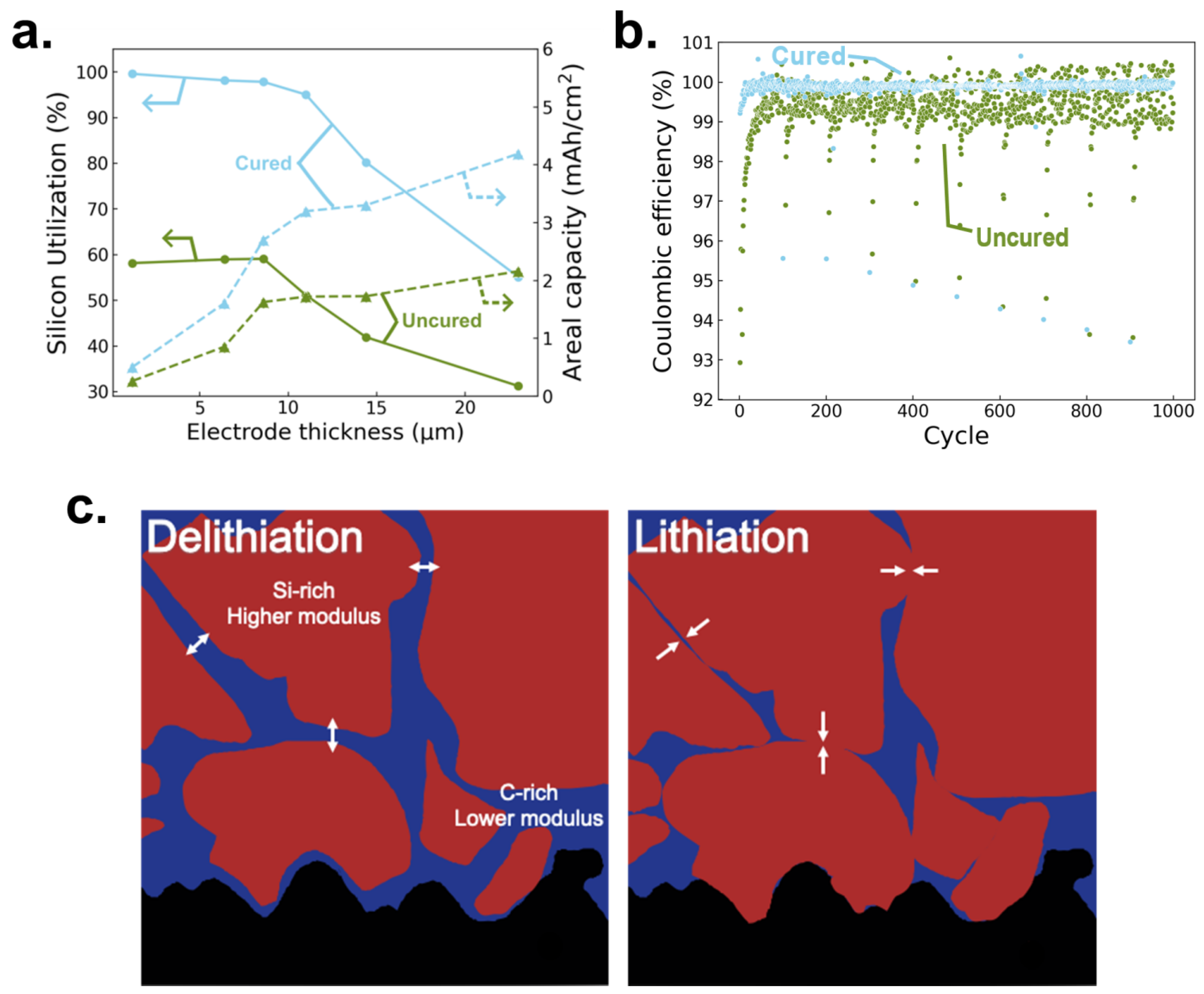
Previous work on Si@PEO electrodes describes their synthesis and demonstrates that the curing step provides significant benefits to electrochemical performance during both short and long-term cycling [7]. As shown in Figure 6a, the third-cycle areal capacity improves with curing for all electrode thicknesses. While areal capacity increases with increasing film thickness, the Si utilization decreases with increasing film thickness, from nearly 100% in very thin electrodes (<6 μm) to roughly 55% in 25 μm thick electrodes, changing in a wide range of Si utilization. The Si utilization is measured by the delithiation capacity of each sample after the third cycle divided by the calculated theoretical delithiation capacity of that sample, assuming Si delithiation capacity to be 3.5 A h g−1 and corrected for PEO mass loss. This trend (decreasing utilization with increasing thickness) is observed for both cured and uncured electrodes.
The first cycle Coulombic efficiency (CE) in a full cell (Figure 5b) improves from 42% in an uncured electrode to 73% in a cured electrode [7]. Within the first 50 cycles, the CE in cured electrodes remains stable at ≥99.75% in most data points. For uncured electrodes, there is significant variation in the CE throughout the first 1000 cycles, averaging between roughly 97.0–100.5% for the C/3 cycles. Cycling data for these specific electrodes in 1–25 cycles without C/10 cycling, which shows the same behavior, can be found in Figure S5.
These improvements in both utilization and CE are attributed to several mechanisms, including the formation of thinner and more inorganic materials on the cured electrodes and increased porosity from PEO removal during curing, which is observed during thermogravimetric analysis (TGA) [7]. Further, as the relationship between electrode morphology and both electronic conductivity and mechanical properties has been discussed above, the impacts of the curing-induced morphological, electrical, and mechanical changes to the cycling performance here should be considered as well [42,43,44].
The carbon-rich bands may provide mechanisms for improving the Si utilization and areal capacity by increasing electronic access to the silicon as compared to more uniformly distributed carbon. Recent work has demonstrated that resistivity distribution and conductive carbon morphology through electrode cross-sections have a clear link to Si utilization [45].
Cross-sectional SSRM images of cured 1 µm- and 6 µm-thick electrodes (Figure S1) showed similar phase segregation with the low-resistivity carbon particles clustering together. However, due to the differences in electrode thickness, the carbon bands do not necessarily result in the same behavior in the thinner electrodes. Many of the Si-rich islands surrounded by carbon in the thick electrodes are larger than the total thin electrode thickness (6 μm). In the thin electrodes, the carbon bands are extremely effective at maximizing Si utilization, but as the electrode thickness increases, there is a less connected network of carbon-rich bands to the current collector through electrical percolation, and some Si remains electrically isolated. This variation in bands with electrode thickness suggests that controlling the carbon-rich band sizes or density with increasing electrode thickness or increasing carbon-Si ratio may be a route to improve electrode performance to accommodate increased areal capacity.
Full cell cycling of Si@PEO electrodes for 1000 cycles (Figure 6b) shows improved CE in the cured sample compared to uncured electrodes. The volumetric expansion of Si that occurs during lithiation induces high strain within electrodes, leading to capacity fade due to fracture and associated active material isolation [46]. While increased porosity is believed to contribute to improved cycling performance, this study identifies another possible mechanism for improved cycling: the low-modulus carbon-rich bands shown in the CR-FV maps of cured electrodes allow for strain relief during expansion by preferentially compressing while still maintaining electrical contact, as shown in Figure 6c [7,17]. Mechanical failure leading to the isolation and loss of active material is known to be a source of capacity fade in electrodes, particularly those made of Si [47,48]. This strain relief adds flexibility to the electrode and prevents the Si-rich regions from mechanical delamination and subsequent electrical connectivity loss to the electrode, thereby preventing capacity fade [49]. Additionally, the carbon-rich regions may help maintain electronic contact as well, aiding in preventing electronic isolation of the Si.

4. Conclusions

This study characterizes composite Si@PEO electrodes using SSRM, CR-FV, SEM-EDS, and nanoindentation, demonstrating that thermal curing results in a phase-segregated morphology in pristine electrodes with carbon-rich bands surrounded by silicon. This morphology is distinct from the uncured electrodes, which have relatively uniformly distributed carbon clusters in a Si matrix. These carbon-rich bands and associated electrical conductivity were preserved after cycling. In contrast, the elastic moduli of the cycled cured electrode changed distinctly, with a much larger modulus of the Si-rich island than the surrounding carbon band, by cycling compared to the uniform modulus distribution in the pristine electrode. While multiple variables can impact electrochemical performance, these two factors—electrical conduction and modulus contrast—can improve electrochemical performance, where the carbon-rich bands provide a Si deformation buffer and electrical pathway. This work further indicates that engineering similar morphologies may be an avenue for mitigating capacity loss issues in other silicon electrode systems.

5. Experimental Details

5.1. Electrode and Cell Fabrication and Cycling

Complete electrode and cell fabrication details can be found in Schulze et al. [7]. Briefly, all electrodes are fabricated with PECVD Si NPs. The Si NPs were surface functionalized in solution with PEO while heating, then purified in toluene and dried back to a powder form. The powder was then mixed in NMP with Timcal C45 conductive carbon black and Ensigner Polyimide P84 binder (8:1:1 Si:C45:P84 by weight). This slurry was blade cast on a copper current collector and dried under vacuum in an oven at 150 °C. The cured electrodes were heated to 420 °C over 1 h under N2; then, the temperature was held at 420 °C for 1 h. This thermal processing also removed PEO attached to the Si NP [7]
Electrodes were assembled in full cell 2032 coin format against Lithium Nickel Manganese Cobalt Oxide (NMC) 622 cathodes in GenF electrolyte, which is Gen2 (1.2 M lithium hexafluorophosphate (LiPF6) in ethylene carbonate (EC): ethyl methyl carbonate (EMC) (3:7 by wt%)) plus 10 wt% fluoroethylene carbonate (FEC) additive. Characterized cells were cycled between 4.2 and 3.0 V at a C/3rate for 25 cycles.

5.2. SEM-EDS

Cross-section samples were made by sandwiching electrodes coated on copper foil between silicon wafers with EpoTek conductive epoxy. The samples were then polished under an argon ion beam of 5 kV energy and ~150 mA current using a JEOL cooling cross-section polisher (JEOL CCP).
SEM-EDS images were collected with a Hitachi S-4800 SEM with an accelerating voltage of 9 kV.

5.3. FIB-EDS for Air-Free Sample Transfer and Element Mapping

EDS was taken using the Nova 200 Dual-beam focused ion beam (FIB) with a Thermofisher UtraDry EDS detector and an air-free transfer station attached. EDS data were taken at both 10 kV and 20 kV using standard dual beam FIB methods. All SEM imaging was acquired at 5 kV. The samples were loaded into an airtight transfer station inside an Ar glovebox. The transfer station was then attached to the FIB. Once the instrument reached an acceptable vacuum level, the transfer station was opened, and the sample was transferred into the instrument for imaging.

5.4. SSRM

SSRM measures the total resistance between the probe and back contact, including the sample spreading resistance (Rsp), probe/sample contact resistance (Rc), and back contact resistance (Rb). Rb is very small compared to Rsp and Rc because of the large contact area. Rc is minimized using high enough forces (~mN) that probe contact is maintained so that the measured resistance is dominated by Rsp, which is further dominated by the local sample resistivity beneath the probe [50].
SSRM measurements were taken using a Bruker Dimension Icon AFM with an SSRM module installed in an Ar-filled glovebox. Bruker DDESP-V2 conductive diamond-coated Si probes were used in AFM contact mode with a −0.25 V bias voltage applied to the sample while the probe was floating-grounded. The data were processed using Bruker Nanoscope (version 2.0), Gwyddion (version 2.54), and ImageJ software (version 1.54).

5.5. CR-FV

CR measures nm-scale viscoelastic properties [18]. By vibrating the sample at a selected frequency range and then measuring the resonant frequencies induced in the probe/sample system, the mechanical properties such as loss modulus and storage modulus are calculated by comparing to a known reference sample made of Al, Cr, and Si. CR calculations combine two mechanical models: (i) Euler–Bernoulli beam theory to relate tip/sample resonant frequency to the stiffness between the tip and sample, and (ii) a combination of Hertz and Derjaguin–Muller–Toporov (DMT) contact models to relate the tip-sample stiffness and the sample modulus [18,19,24,51,52].
The second mechanical mapping method used, FV, records the force–distance (f–z) curve of the AFM tip as it approaches the sample, interacts with the Van der Waals forces of the sample surface, contacts the sample with a repulsion force, and lifts off [19]. Analyzing the curve shape determines multiple properties, including modulus during contacting and adhesion during liftoff. Multiple contact mechanics models can be used to model the probe and sample, similar to CR [53].
CR-FV measurements were conducted using the AFM setup described above, using Bruker PeakForce QNM + CR mode and Bruker DDLTESP (k = 95 N/m) probes. CR and FV data were collected simultaneously and processed using Bruker Nanoscope software (version 2.0).

5.6. Nanoindentation

Nanoindentation tests were conducted with a diamond Berkovich indenter tip using a KLA iMicro Nanoindenter inside an inert atmosphere glovebox. Thermal drift during indentation was monitored and remained below 0.1 nm/s. Depth-controlled tests with a constant strain rate of 0.01 s−1 (Hz) were used with a 10 s hold at maximum depth. The target indentation depth was set to be 1000 nm. The Oliver–Pharr method was followed to determine the elastic modulus and hardness of the material at the target depth.

Supplementary Materials

The following supporting information can be downloaded at: https://www.mdpi.com/article/10.3390/batteries10090313/s1, Figure S1: SSRM maps for 1 and 6 µm-thick cured pristine electrodes, showing that carbon segregation is present in thinner electrodes; Figure S2: CR-FV and corresponding height map for pristine uncured sample. A low and uniform overall modulus is observed; Figure S3: Additional CR-FV and corresponding height maps of the cured cycled sample showing high modulus islands surrounded by lower modulus domains; Figure S4: Contact resonance frequency curves showing higher and cleaner resonant frequency peaks for the high modulus domain (1) and lower and noisier peaks for the low modulus domain; Figure S5: Cycling for the cured and uncured data over 25 cycles for the electrodes characterized in this work; Table S1: Area percentages of identified domains from resistivity maps compared to calculated volume percentage to verify accuracy to domain identification.

Author Contributions

Conceptualization, Z.H., G.M.C., N.R.N. and C.J.; methodology, Z.H., J.C., P.W. and C.J.; formal Analysis Z.H., G.M.C., J.C. and P.W.; investigation Z.H., G.M.C., J.C., N.R.N., S.D. and C.J.; data curation Z.H., G.M.C., J.C. and P.W.; writing—original draft preparation, Z.H.; writing—review and editing, G.M.C., J.C., P.W., N.R.N., S.D. and C.J.; supervision, N.R.N., S.D. and C.J. All authors have read and agreed to the published version of the manuscript.

Funding

This research was funded by the U.S. Department of Energy’s Vehicle Technologies Office under the Silicon Consortium Project, directed by Brian Cunningham and managed by Anthony Burrell.

Data Availability Statement

The data presented in this study are available on request from the authors.

Acknowledgments

This work was authored in part by the National Renewable Energy Laboratory, operated by the Alliance for Sustainable Energy, LLC, for the U.S. Department of Energy (DOE) under Contract No. DE-AC36-08GO28308. Funding was provided by the U.S. Department of Energy’s Vehicle Technologies Office under the Silicon Consortium Project, directed by Brian Cunningham and managed by Anthony Burrell. The views expressed in the article do not necessarily represent the views of the DOE or the U.S. Government. The U.S. Government retains, and the publisher, by accepting the article for publication, acknowledges that the U.S. Government retains a nonexclusive, paid-up, irrevocable, worldwide license to publish or reproduce the published form of this work or allow others to do so for U.S. Government purposes.

Conflicts of Interest

The authors declare no conflict of interest.

References

  1. Feng, K.; Li, M.; Liu, W.; Kashkooli, A.G.; Xiao, X.; Cai, M.; Chen, Z. Silicon-Based Anodes for Lithium-Ion Batteries: From Fundamentals to Practical Applications. Small 2018, 14, 1702737. [Google Scholar] [CrossRef] [PubMed]
  2. Li, P.; Hwang, J.Y.; Sun, Y.K. Nano/Microstructured Silicon-Graphite Composite Anode for High-Energy-Density Li-Ion Battery. ACS Nano 2019, 13, 2624–2633. [Google Scholar] [CrossRef] [PubMed]
  3. Obrovac, M.N.; Krause, L.J. Reversible Cycling of Crystalline Silicon Powder. J. Electrochem. Soc. 2007, 154, A103. [Google Scholar] [CrossRef]
  4. Peled, E.; Menkin, S. Review—SEI: Past, Present and Future. J. Electrochem. Soc. 2017, 164, A1703–A1719. [Google Scholar] [CrossRef]
  5. Steinruck, H.G.; Cao, C.; Veith, G.M.; Toney, M.F. Toward Quantifying Capacity Losses Due to Solid Electrolyte Interphase Evolution in Silicon Thin Film Batteries. J. Chem. Phys. 2020, 152, 084702. [Google Scholar] [CrossRef]
  6. Nadimpalli, S.P.V.; Sethuraman, V.A.; Dalavi, S.; Lucht, B.; Chon, M.J.; Shenoy, V.B.; Guduru, P.R. Quantifying Capacity Loss Due to Solid-Electrolyte-Interphase Layer Formation on Silicon Negative Electrodes in Lithium-Ion Batteries. J. Power Sources 2012, 215, 145–151. [Google Scholar] [CrossRef]
  7. Schulze, M.C.; Urias, F.; Dutta, N.S.; Huey, Z.; Coyle, J.; Teeter, G.; Doeren, R.; Tremolet de Villers, B.J.; Han, S.-D.; Neale, N.R.; et al. Control of Nanoparticle Dispersion, SEI Composition, and Electrode Morphology Enables Long Cycle Life in High Silicon Content Nanoparticle-Based Composite Anodes for Lithium-Ion Batteries. J. Mater. Chem. A 2023, 11, 5257–5266. [Google Scholar] [CrossRef]
  8. Su, X.; Wu, Q.; Li, J.; Xiao, X.; Lott, A.; Lu, W.; Sheldon, B.W.; Wu, J. Silicon-Based Nanomaterials for Lithium-Ion Batteries: A Review. Adv. Energy Mater. 2014, 4, 1300882. [Google Scholar] [CrossRef]
  9. Mangolini, L.; Thimsen, E.; Kortshagen, U. High-Yield Plasma Synthesis of Luminescent Silicon Nanocrystals. Nano Lett. 2005, 5, 655–659. [Google Scholar] [CrossRef]
  10. Kraytsberg, A.; Ein-Eli, Y. Conveying Advanced Li-Ion Battery Materials into Practice The Impact of Electrode Slurry Preparation Skills. Adv. Energy Mater. 2016, 6, 1600655. [Google Scholar] [CrossRef]
  11. Schulze, M.C.; Carroll, G.M.; Martin, T.R.; Sanchez-Rivera, K.; Urias, F.; Neale, N.R. Hydrophobic versus Hydrophilic Interfacial Coatings on Silicon Nanoparticles Teach Us How to Design the Solid Electrolyte Interphase in Silicon-Based Li-Ion Battery Anodes. ACS Appl. Energy Mater. 2021, 4, 1628–1636. [Google Scholar] [CrossRef]
  12. Weidong, Z.; Wentao, S.; Ling-Zhi, C.; Deyu, W.; Hong, L.; Flemming, B.; Fuqiang, H.; Cai, S. Beyond Imaging: Applications of Atomic Force Microscopy for the Study of Lithium-Ion Batteries. Ultramicroscopy 2019, 204, 34–48. [Google Scholar] [CrossRef]
  13. Stetson, C.; Huey, Z.; Downard, A.; Li, Z.; To, B.; Zakutayev, A.; Jiang, C.S.; Al-Jassim, M.M.; Finegan, D.P.; Han, S.D.; et al. Three-Dimensional Mapping of Resistivity and Microstructure of Composite Electrodes for Lithium-Ion Batteries. Nano Lett. 2020, 20, 8081–8088. [Google Scholar] [CrossRef]
  14. Stetson, C.; Yoon, T.; Coyle, J.; Nemeth, W.; Young, M.; Norman, A.; Pylypenko, S.; Ban, C.; Jiang, C.-S.; Al-Jassim, M.; et al. Three-Dimensional Electronic Resistivity Mapping of Solid Electrolyte Interphase on Si Anode Materials. Nano Energy 2019, 55, 477–485. [Google Scholar] [CrossRef]
  15. Hopkins, E.J.; Frisco, S.; Pekarek, R.T.; Stetson, C.; Huey, Z.; Harvey, S.; Li, X.; Key, B.; Fang, C.; Liu, G. Examining CO2 as an Additive for Solid Electrolyte Interphase Formation on Silicon Anodes. J. Electrochem. Soc. 2021, 168, 030534. [Google Scholar] [CrossRef]
  16. Huey, Z.; Ha, Y.; Frisco, S.; Norman, A.; Teeter, G.; Jiang, C.-S.; DeCaluwe, S.C. Multi-Modal Characterization Methods of Solid-Electrolyte Interphase in Silicon-Graphite Composite Electrodes. J. Power Sources 2023, 564, 232804. [Google Scholar] [CrossRef]
  17. Kim, S.H.; Kim, Y.S.; Baek, W.J.; Heo, S.; Yun, D.J.; Han, S.; Jung, H. Nanoscale Electrical Degradation of Silicon-Carbon Composite Anode Materials for Lithium-Ion Batteries. ACS Appl. Mater. Interfaces 2018, 10, 24549–24553. [Google Scholar] [CrossRef]
  18. Yuya, P.A.; Hurley, D.C.; Turner, J.A. Contact-Resonance Atomic Force Microscopy for Viscoelasticity. J. Appl. Phys. 2008, 104, 074916. [Google Scholar] [CrossRef]
  19. Killgore, J.P.; Yablon, D.G.; Tsou, A.H.; Gannepalli, A.; Yuya, P.A.; Turner, J.A.; Proksch, R.; Hurley, D.C. Viscoelastic Property Mapping with Contact Resonance Force Microscopy. Langmuir 2011, 27, 13983–13987. [Google Scholar] [CrossRef]
  20. Goldstein, J.I.; Newbury, D.E.; Michael, J.R.; Ritchie, N.W.M.; Scott, J.H.J.; Joy, D.C. X-rays. In Scanning Electron Microscopy and X-ray Microanalysis; Springer: New York, NY, USA, 2018; pp. 39–63. ISBN 978-1-4939-6674-5. [Google Scholar]
  21. Heiskanen, S.K.; Kim, J.; Lucht, B.L. Generation and Evolution of the Solid Electrolyte Interphase of Lithium-Ion Batteries. Joule 2019, 3, 2322–2333. [Google Scholar] [CrossRef]
  22. Burdette-Trofimov, M.K.; Armstrong, B.L.; Heroux, L.; Doucet, M.; Márquez Rossy, A.E.; Hoelzer, D.T.; Kanbargi, N.; Naskar, A.K.; Veith, G.M. Competitive Adsorption within Electrode Slurries and Impact on Cell Fabrication and Performance. J. Power Sources 2022, 520, 230914. [Google Scholar] [CrossRef]
  23. Dimension Icon User Guide. Available online: https://www.nanophys.kth.se/nanolab/afm/icon/bruker-help/Content/Cover%20page.htm (accessed on 4 March 2024).
  24. Zhou, X.; Fu, J.; Li, F. Contact Resonance Force Microscopy for Nanomechanical Characterization: Accuracy and Sensitivity. J. Appl. Phys. 2013, 114, 064301. [Google Scholar] [CrossRef]
  25. Zhang, Z.; Smith, K.; Jervis, R.; Shearing, P.R.; Miller, T.S.; Brett, D.J.L. Operando Electrochemical Atomic Force Microscopy of Solid-Electrolyte Interphase Formation on Graphite Anodes: The Evolution of SEI Morphology and Mechanical Properties. ACS Appl. Mater. Interfaces 2020, 12, 35132–35141. [Google Scholar] [CrossRef]
  26. Zheng, J.; Liu, J.; Wang, S.; Luo, F.; Ben, L.; Li, H. Influence of Fluoroethylene Carbonate on the Solid Electrolyte Interphase of Silicon Anode for Li-Ion Batteries: A Scanning Force Spectroscopy Study. Chin. Phys. B 2020, 29, 048203. [Google Scholar] [CrossRef]
  27. McBrayer, J.D.; Apblett, C.A.; Harrison, K.L.; Fenton, K.R.; Minteer, S.D. Mechanical Studies of the Solid Electrolyte Interphase on Anodes in Lithium and Lithium Ion Batteries. Nanotechnology 2021, 32, 502005. [Google Scholar] [CrossRef]
  28. Lin, E.Y.; Frischknecht, A.L.; Riggleman, R.A. Chain and Segmental Dynamics in Polymer–Nanoparticle Composites with High Nanoparticle Loading. Macromolecules 2021, 54, 5335–5343. [Google Scholar] [CrossRef]
  29. Odegard, G.M.; Clancy, T.C.; Gates, T.S. Modeling of the Mechanical Properties of Nanoparticle/Polymer Composites. Polymer 2005, 46, 553–562. [Google Scholar] [CrossRef]
  30. Hurley, D.C. Contact Resonance Force Microscopy Techniques for Nanomechanical Measurements. In Applied Scanning Probe Methods; Bhushan, B., Fuchs, H., Eds.; Springer-Verlag: Berlin/Heidelberg, Germany; New York, NY, USA, 2009; Volume XI, pp. 97–138. [Google Scholar]
  31. Rabe, U.; Kopycinska, M.; Hirsekorn, S.; Arnold, W. Evaluation of the Contact Resonance Frequencies in Atomic Force Microscopy as a Method for Surface Characterisation (Invited). Ultrasonics 2002, 40, 49–54. [Google Scholar] [CrossRef]
  32. Stan, G.; Cook, R.F. Mapping the Elastic Properties of Granular Au Films by Contact Resonance Atomic Force Microscopy. Nanotechnology 2008, 19, 235701. [Google Scholar] [CrossRef]
  33. Polyimide P84NT Technical Brochure. Available online: https://www.pp-evonik.com/assets/img/uploads/Evonik%20Polyimide%20P84NT%20technical%20brochure%20A4.pdf (accessed on 9 February 2024).
  34. TECAPOWDER PI—Polyimide Powder from Ensinger. Available online: https://www.ensingerplastics.com/en/thermoplastic-materials/pi-polyimide/polyimide-powder (accessed on 9 February 2024).
  35. Rosenberger, M.R.; Chen, S.; Prater, C.B.; King, W.P. Micromechanical Contact Stiffness Devices and Application for Calibrating Contact Resonance Atomic Force Microscopy. Nanotechnology 2017, 28, 044003. [Google Scholar] [CrossRef]
  36. Pittenger, B.; Yablon, D. Improving the Accuracy of Nanomechanical Measurements with Force-Curve-Based AFM Techniques. Bruker Appl. Notes 2017, 1, 1–7. [Google Scholar]
  37. Ma, C.; Wang, W.; Chen, Y.; Arnold, W.; Chu, J. Depth-Sensing Using AFM Contact-Resonance Imaging and Spectroscopy at the Nanoscale. J. Appl. Phys. 2019, 126, 124302. [Google Scholar] [CrossRef]
  38. Freund, L.B.; Suresh, S. Film Stress and Substrate Curvature. In Thin Film Materials: Stress, Defect Formation, and Surface Evolution; Cambridge University Press: Cambridge, UK; New York, NY, USA, 2003. [Google Scholar]
  39. Guo, D.; Xie, G.; Luo, J. Mechanical Properties of Nanoparticles: Basics and Applications. J. Phys. D Appl. Phys. 2014, 47, 013001. [Google Scholar] [CrossRef]
  40. Nam, K.-H.; Hwa Chae, K.; Choi, J.-H.; Jeon, K.-J.; Park, C.-M. Superior Carbon Black: High-Performance Anode and Conducting Additive for Rechargeable Li- and Na-Ion Batteries. Chem. Eng. J. 2021, 417, 129242. [Google Scholar] [CrossRef]
  41. Liu, S.; Zeng, X.; Liu, D.; Wang, S.; Zhang, L.; Zhao, R.; Kang, F.; Li, B. Understanding the Conductive Carbon Additive on Electrode/Electrolyte Interface Formation in Lithium-Ion Batteries via in Situ Scanning Electrochemical Microscopy. Front. Chem. 2020, 8, 114. [Google Scholar] [CrossRef]
  42. Madzvamuse, A.; Hamenu, L.; Mohammed, L.; Ko, J.M. Effect of Morphologically Different Conductive Agents on the Performance of Silicon Anode in Lithium-Ion Batteries. ChemistrySelect 2018, 3, 10805–10810. [Google Scholar] [CrossRef]
  43. Jia, H.; Li, X.; Song, J.; Zhang, X.; Luo, L.; He, Y.; Li, B.; Cai, Y.; Hu, S.; Xiao, X.; et al. Hierarchical Porous Silicon Structures with Extraordinary Mechanical Strength as High-Performance Lithium-Ion Battery Anodes. Nat. Commun. 2020, 11, 1474. [Google Scholar] [CrossRef] [PubMed]
  44. Magri, M.; Boz, B.; Cabras, L.; Salvadori, A. Quantitative Investigation of the Influence of Electrode Morphology in the Electro-Chemo-Mechanical Response of Li-Ion Batteries. Electrochim. Acta 2022, 405, 139778. [Google Scholar] [CrossRef]
  45. Kim, J.H.; Huey, Z.; Veith, G.M.; Jiang, C.-S.; Neale, N.R.; Carroll, G.M. Blended 1D Carbon Nanostructures Synergistically Enhance Electron and Ion Transport in Silicon Nanoparticle Electrodes. Cell Rep. Phys. Sci. 2024, 5, 101974. [Google Scholar] [CrossRef]
  46. Kumar, R.; Woo, J.H.; Xiao, X.; Sheldon, B.W. Internal Microstructural Changes and Stress Evolution in Silicon Nanoparticle Based Composite Electrodes. J. Electrochem. Soc. 2017, 164, A3750–A3765. [Google Scholar] [CrossRef]
  47. Zhang, W.-J. A Review of the Electrochemical Performance of Alloy Anodes for Lithium-Ion Batteries. J. Power Sources 2011, 196, 13–24. [Google Scholar] [CrossRef]
  48. Li, D.; Wang, Y.; Hu, J.; Lu, B.; Cheng, Y.-T.; Zhang, J. In Situ Measurement of Mechanical Property and Stress Evolution in a Composite Silicon Electrode. J. Power Sources 2017, 366, 80–85. [Google Scholar] [CrossRef]
  49. Wang, H.; Lu, S.-H.; Wang, X.; Xia, S.; Beng Chew, H. A Review of the Multiscale Mechanics of Silicon Electrodes in High-Capacity Lithium-Ion Batteries. J. Phys. D Appl. Phys. 2021, 55, 063001. [Google Scholar] [CrossRef]
  50. Eyben, P.; Vandervorst, W.; Alvarez, D.; Xu, M.; Fouchier, M. Probing Semiconductor Technology and Devices with Scanning Spreading Resistance Microscopy. In Scanning Probe Microscopy: Electrical and Electromechanical Phenomena at the Nanoscale; Kalinin, S., Gruverman, A., Eds.; Springer: New York, NY, USA, 2007; pp. 31–87. ISBN 978-0-387-28668-6. [Google Scholar]
  51. Wagner, R.; Moon, R.J.; Raman, A. Mechanical Properties of Cellulose Nanomaterials Studied by Contact Resonance Atomic Force Microscopy. Cellulose 2016, 23, 1031–1041. [Google Scholar] [CrossRef]
  52. Derjaguin, B.V.; Muller, V.M.; Toporov, Y.P. Effect of Contact Deformations on the Adhesion of Particles. J. Colloid Interface Sci. 1975, 53, 314–326. [Google Scholar] [CrossRef]
  53. Cappella, B.; Dietler, G. Force-Distance Curves by Atomic Force Microscopy. Surf. Sci. Rep. 1999, 34, 1–104. [Google Scholar] [CrossRef]
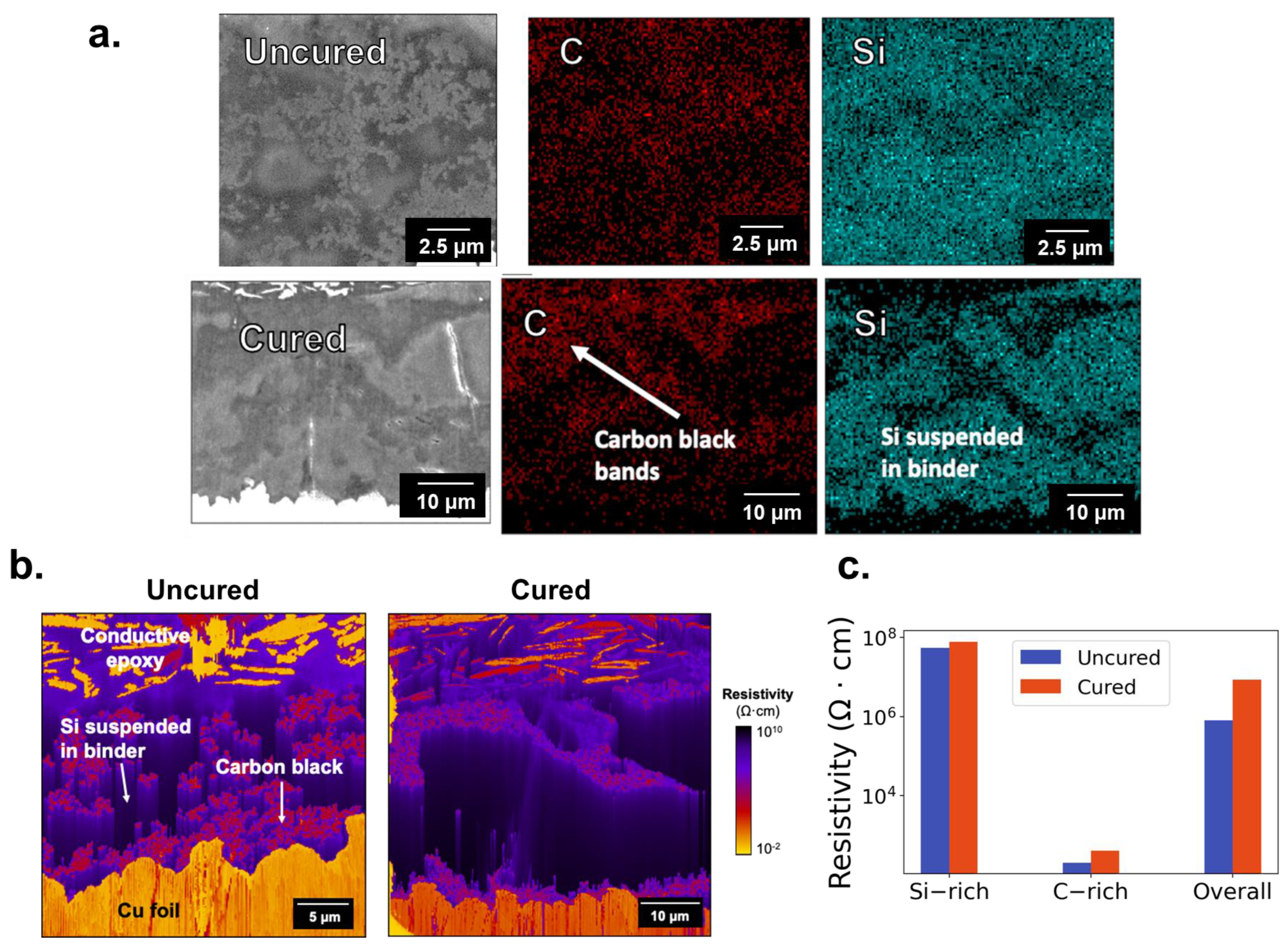
Figure 1. (a) SEM-EDS images of electrode cross sections, with the uncured sample showing uniform carbon and Si distribution through thickness, while the cured electrode has an alternating carbon-rich and Si-rich band structure. (b) SSRM resistivity maps of an uncured and cured electrode showing the lower-resistivity C45 particles segregated into bands by curing. (c) Measured resistivity values of the Si and carbon-rich domains, which do not change significantly by curing. Figure 1b is reproduced from Ref. [7] with permission from the Royal Society of Chemistry.
Batteries 10 00313 g001
Figure 2. (a) Optical micrograph showing nanoindents in pristine cured electrode cross section and (b) overlay of height map and SSRM resistivity map after nanoindentation used to designate phase of each indent. (c) Resulting nanoindentation modulus values for individual phases. (d) FV, (e) CR, and (f) corresponding height map for pristine cured electrode cross-section, showing no clear mechanical property variation through electrode thickness.
Batteries 10 00313 g002
Figure 3. Images of uncured electrodes after 25 cycles showing (a) SSRM resistivity map and corresponding (b) FV, (c) CR, and (d) height maps showing uniform resistivity and mechanical properties through electrode thickness. Both measurements show no distinct domains, consistent with images of the uncured pristine electrode showing homogeneous component distribution.
Batteries 10 00313 g003
Figure 4. (a) SEM-EDS, (b) SSRM of multiple sites, and (c) FV, (d) CR, and (e) corresponding height maps of the cycled cured sample showing carbon and Si segregation and its impacts on resistivity and mechanical properties. All maps show domains with distinct properties matching the carbon segregation observed in cured pristine electrodes.
Batteries 10 00313 g004
Figure 5. Data from CR scan of cured cycled sample including (a) height map, (b) CR data fit adjusted to both high and low modulus curves (white means no fit obtained), (c) CR data fit adjusted to the high modulus domain only, showing distinct island features, (d) overlay of b and c showing high and low modulus domains, (e) software-generated fill of b to more clearly show modulus domains, and (f) CR frequency curve amplitude map that also shows variation between high and low modulus domains.
Batteries 10 00313 g005
Figure 6. (a) Areal capacity and silicon utilization vs. electrode thickness for uncured and cured electrodes. (b) Coulombic efficiency for uncured and cured electrodes over 1000 cycles. Si@PEO electrodes were cycled against NMC811 between 4.2 and 3.0 V for 99 cycles at C/3 and 1 cycle at C/10 10 times. The C/10 cycles were used to distinguish Li+ transport limitations from irreversible processes. (c) Schematic diagram of how the lower modulus of the carbon-rich domains may provide strain relief during Si expansion/compression during lithiation/delithiation. Arrows indicate expansion and contraction of active Si material island during lithiation/delithiation. (a,b) Reproduced from Ref. [9] with permission from the Royal Society of Chemistry.
Batteries 10 00313 g006
Table 1. Average CR-FV modulus values for all samples.
SampleUncycledCycled
FV Modulus (GPa)CR Modulus (GPa)FV Modulus (GPa)CR Modulus (GPa)
Uncured7.757.6673.341.0
Cured11.28.506.63 (low)10.9 (low)
48.2 (high)43.7 (high)
Disclaimer/Publisher’s Note: The statements, opinions and data contained in all publications are solely those of the individual author(s) and contributor(s) and not of MDPI and/or the editor(s). MDPI and/or the editor(s) disclaim responsibility for any injury to people or property resulting from any ideas, methods, instructions or products referred to in the content.