
Ferromagnetic Resonance of a [GeTe/Sb2Te3]6/Py Superlattice


Abstract
:1. Introduction
2. Methods
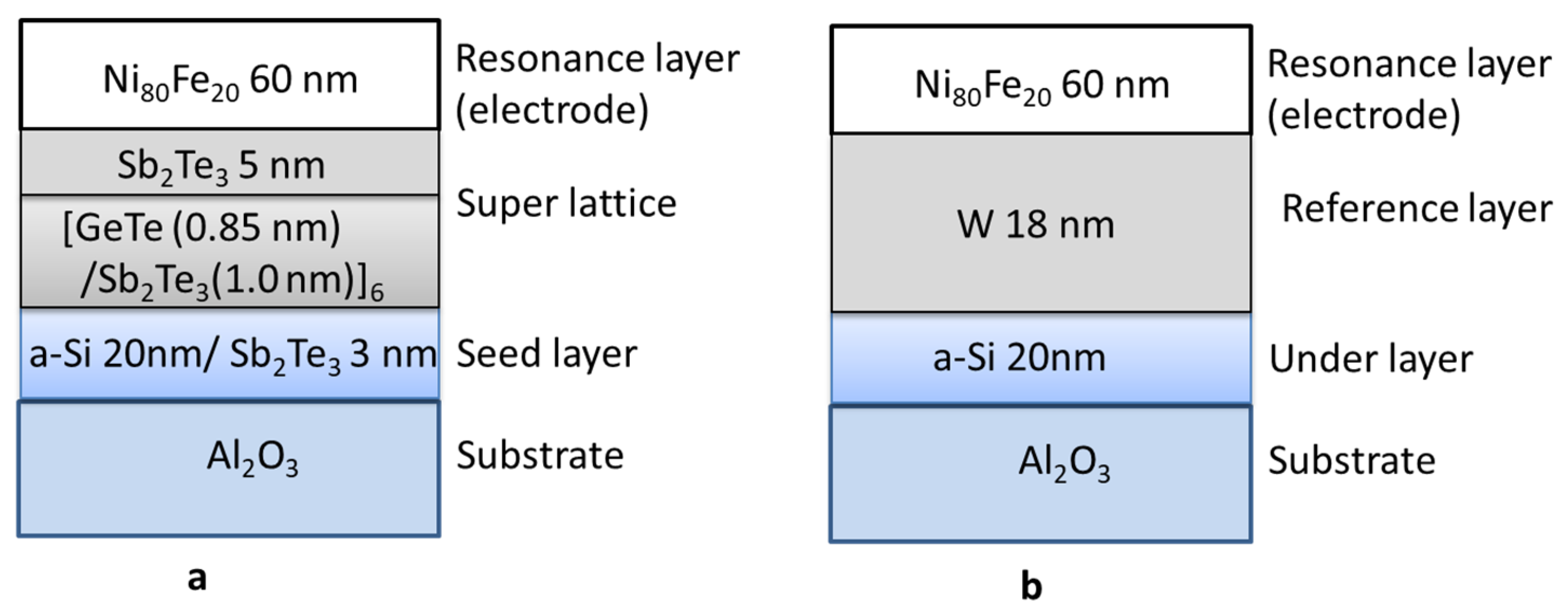
2.1. Fabrication of the Films
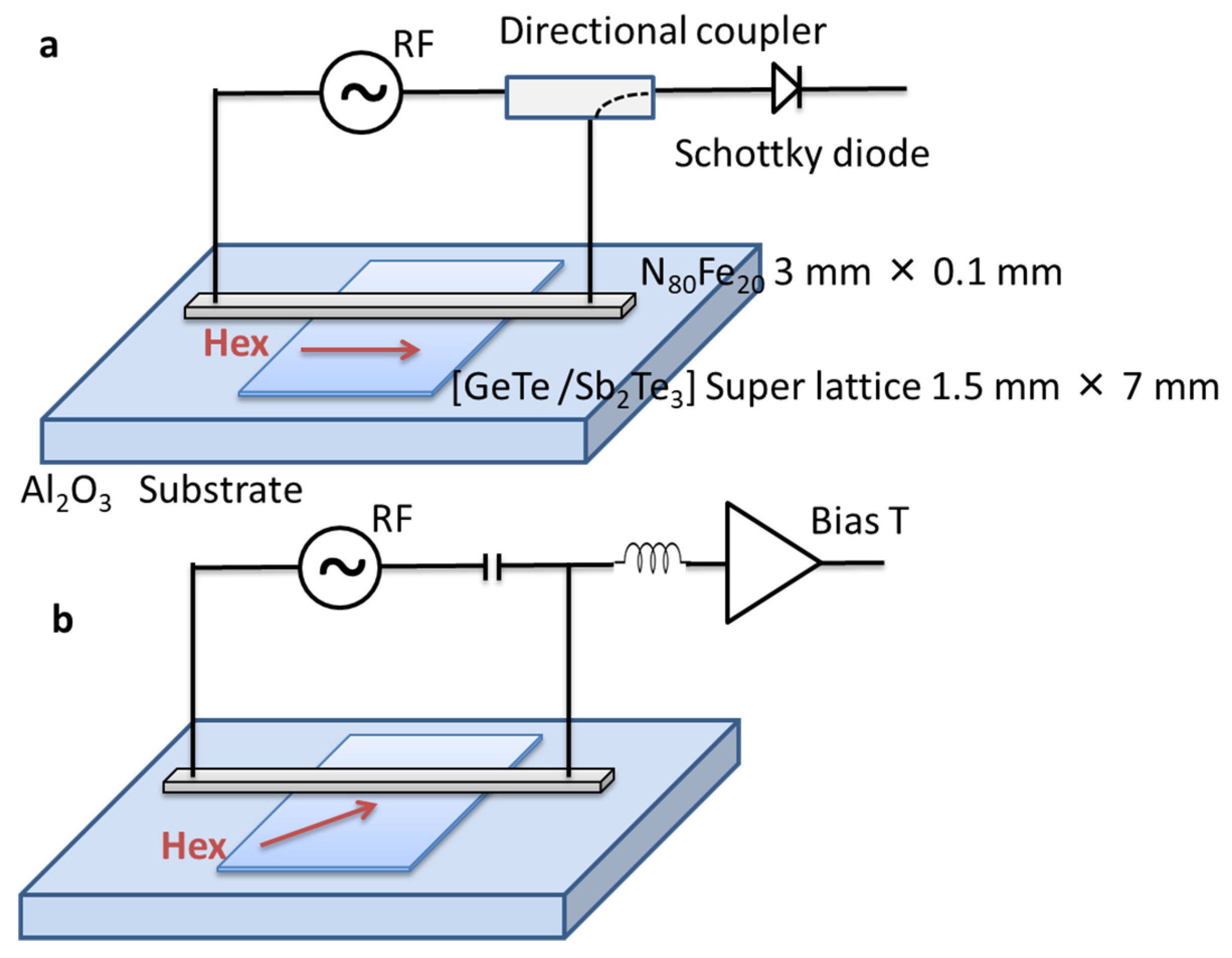
2.2. Measurement
3. Results
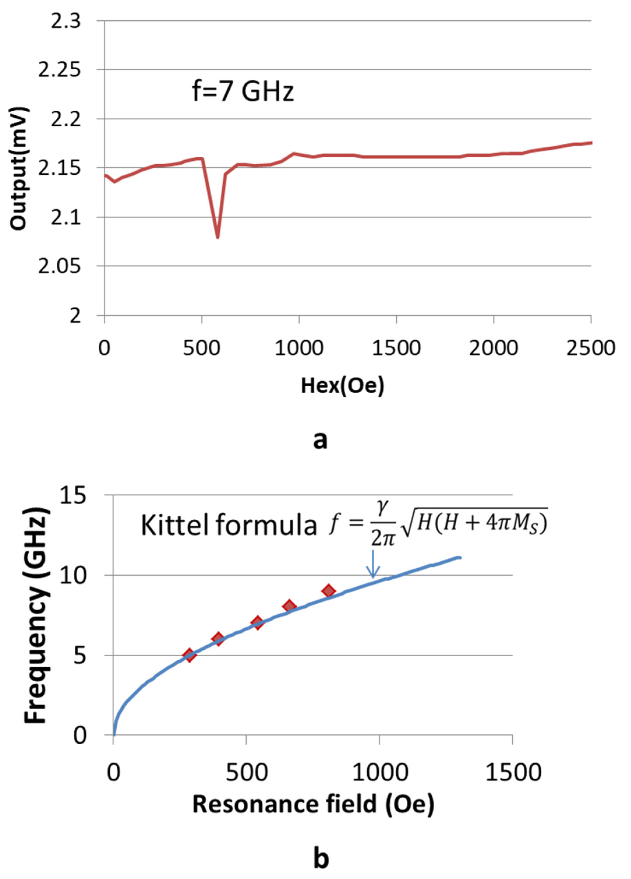
3.1. Normal FMR
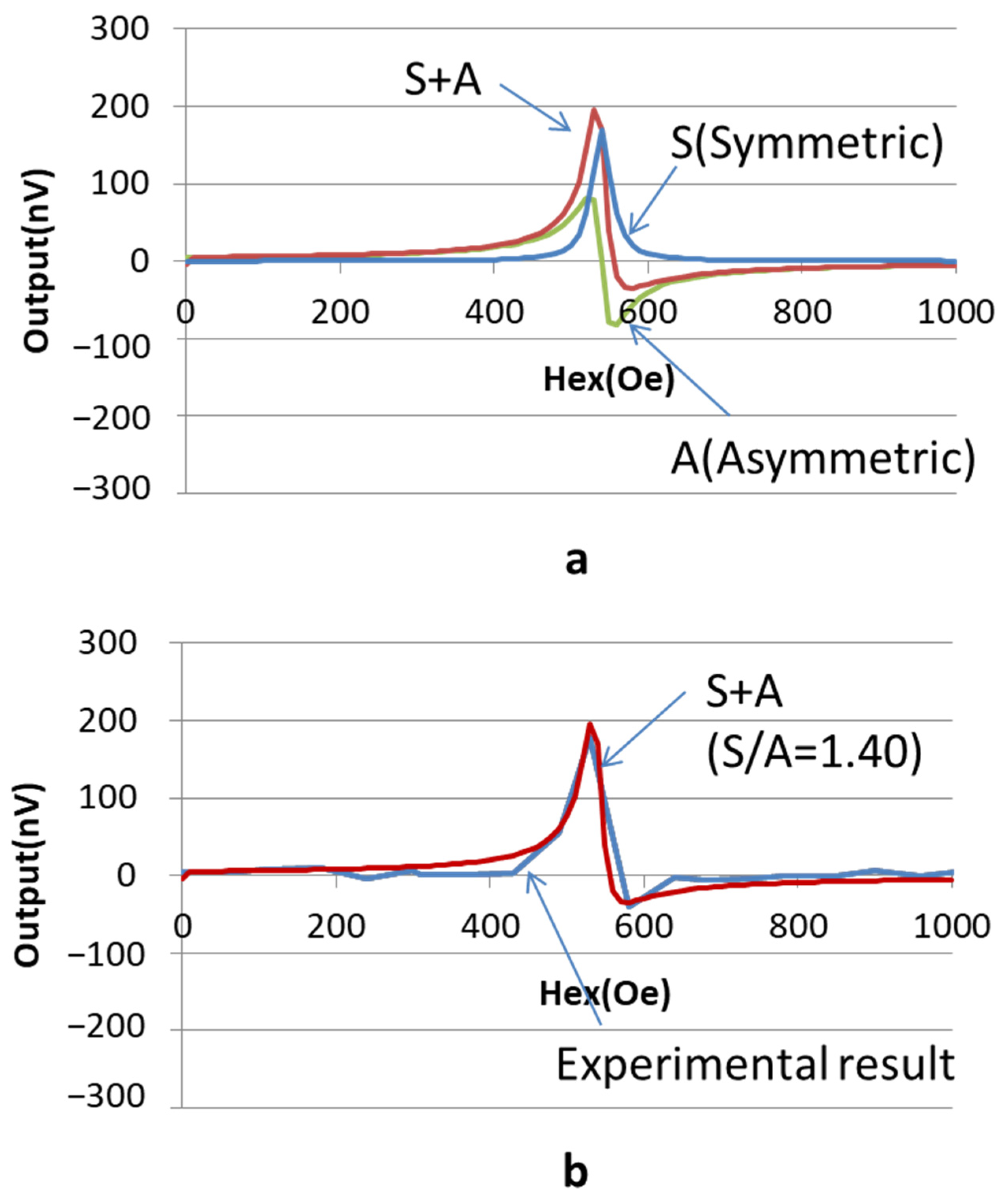
3.2. ST-FMR
4. Discussions
Author Contributions
Funding
Data Availability Statement
Conflicts of Interest
References
- Moore, J.E. The birth of topological insulator. Nature 2010, 464, 194–198. [Google Scholar] [CrossRef] [PubMed]
- Bernevig, B.A.; Hughes, T.L.; Zhang, S.-C. Topological Phase Transition in HgTe Quantum Wells. Science 2006, 314, 1757–1761. [Google Scholar] [CrossRef] [PubMed] [Green Version]
- Hsieh, D.; Qian, D.; Wray, L.; Xia, Y.; Hor, Y.S.; Cava, R.J.; Hasan, M.Z. A topological Dirac insulator in a quantum spin Hall phase. Nature 2008, 452, 970–974. [Google Scholar] [CrossRef] [PubMed] [Green Version]
- Xia, Y.; Qian, D.; Hsieh, D.; Wray, L.A.; Pal, A.; Lin, H.; Bansil, A.; Grauer, D.; Hor, Y.S.; Cava, R.J.; et al. Observation of a large-gap topological-insulator class with a single Dirac cone on the surface. Nat. Phys. 2009, 5, 398–402. [Google Scholar] [CrossRef] [Green Version]
- Hsieh, D.; Xia, Y.; Qian, D.; Wray, L.; Dil, J.H.; Meier, F.; Osterwalder, J.; Patthey, L.; Checkelsky, J.G.; Ong, N.P.; et al. A tunable topological insulator in the spin helical Dirac transport regime. Nature 2009, 460, 1101–1106. [Google Scholar] [CrossRef] [Green Version]
- Hsieh, D.; Xia, Y.; Qian, D.; Wray, L.; Meier, F.; Dil, J.H.; Osterwalder, J.; Patthey, L.; Fedorov, A.V.; Lin, H.; et al. Observation of time-reversal-projected single-Dirac-cone topological-insulator states in Bi2Te3 and Sb2Te3. Phys. Rev. Lett. 2009, 103, 146401. [Google Scholar] [CrossRef] [PubMed] [Green Version]
- Zhang, H.; Liu, C.-X.; Qi, X.-L.; Dai, X.; Fang, Z.; Zhang, S.-C. Topological insulators in Bi2Se3, Bi2Te3 and Sb2Te3 with a single Dirac cone on the surface. Nat. Phys. 2009, 5, 438–442. [Google Scholar] [CrossRef]
- Kifune, K.; Kubota, Y.; Matsunaga, T.; Yamada, N. Extremely long period-stacking structure in the Sb–Te binary system. Acta Crystallogr. Sect. B Struct. Sci. 2005, 61, 492–497. [Google Scholar] [CrossRef]
- Kim, M.; Kim, C.H.; Kim, H.-S.; Ihm, J. Topological quantum phase transitions driven by external electric fields in Sb2Te3 thin films. Proc. Natl. Acad. Sci. USA 2012, 109, 671–674. [Google Scholar] [CrossRef] [Green Version]
- Burkov, A.A.; Hawthorn, D.G. Spin and Charge Transport on the Surface of a Topological Insulator. Phys. Rev. Lett. 2010, 105, 066802. [Google Scholar] [CrossRef] [PubMed] [Green Version]
- Culcer, D.; Hwang, E.H.; Stanescu TDSarma, S.D. Two-dimensional surface charge transport in topological insulators. Phys. Rev. B 2010, 82, 155457. [Google Scholar] [CrossRef] [Green Version]
- Pesin, D.; MacDonald, A. Spintronics and pseudospintronics in graphene and topological insulators. Nat. Mater. 2012, 11, 409–416. [Google Scholar] [CrossRef] [PubMed]
- Mellnik, A.R.; Lee, J.S.; Richardella, A.; Grab, J.; Mintun, P.J.; Fischer, M.H.; Vaezi, A.; Manchon, A.; Kim, E.-A.; Samarth, N.; et al. Spin-transfer torque generated by a topological insulator. Nat. Cell Biol. 2014, 511, 449–451. [Google Scholar] [CrossRef] [PubMed]
- Gervacio-Arciniega, J.J.; Prokhorov, E.; Espinoza-Beltrán, F.J.; Trapaga, G. Characterization of local piezoelectric behavior of ferroelectric GeTe and Ge2Sb2Te5 thin films. J. Appl. Phys. 2012, 112, 052018. [Google Scholar] [CrossRef]
- E Simpson, R.; Fons, P.; Kolobov, A.V.; Fukaya, T.; Krbal, M.; Yagi, T.; Tominaga, J. Interfacial phase-change memory. Nat. Nanotechnol. 2011, 6, 501–505. [Google Scholar] [CrossRef]
- Tominaga, J.; Kolobov, A.V.; Fons, P.J.; Wang, X.; Saito, Y.; Nakano, T.; Hase, M.; Murakami, S.; Herfort, J.; Takagaki, Y.; et al. Giant multiferroic effects in topological GeTe-Sb2Te3 superlattices. Sci. Technol. Adv. Mater. 2015, 16, 014402. [Google Scholar] [CrossRef] [PubMed]
- Tominaga, J.; Kolobov, A.V.; Fons, P.; Nakano, T.; Murakami, S. Ferroelectric Order Control of the Dirac-Semimetal Phase in GeTe-Sb2Te3 Superlattices. Adv. Mater. Interfaces 2014, 1, 1300027. [Google Scholar] [CrossRef]
- Tominaga, J.; Simpson, R.E.; Fons, P.; Kolobov, A.V. Electrical-field induced giant magnetoresistivity in (non-magnetic) phase change films. Appl. Phys. Lett. 2011, 99, 152105. [Google Scholar] [CrossRef] [Green Version]
- Bang, D.; Awano, H.; Tominaga, J.; Kolobov, A.V.; Fons, P.; Saito, Y.; Makino, K.; Nakano, T.; Hase, M.; Takagaki, Y.; et al. Mirror-symmetric Magneto-optical Kerr Rotation using Visible Light in [(GeTe)2(Sb2Te3)1]n Topological Superlattices. Sci. Rep. 2014, 4, 5727. [Google Scholar] [CrossRef] [Green Version]
- Sumi, S.; Awano, H.; Tominaga, J. Magneto-Capacitance of [GeTe/Sb2Te3] Supper Lattice Film; e-PCOS 2017 PC-09; Aachen, Germany, 2017. [Google Scholar]
- Sa, B.; Zhou, J.; Sun, Z.; Tominaga, J.; Ahuja, R. Topological Insulating in GeTe/Sb2Te3 Phase-Change Superlattice. Phys. Rev. Lett. 2012, 109, 096802. [Google Scholar] [CrossRef]
- Tominaga, J.; Miyata, N.; Sumi, S.; Awano, H.; Murakami, S. Topologically protected spin diffusion and spin generator using chalcogenide superlattices. NPJ 2D Mater. Appl. 2020, 4, 22. [Google Scholar] [CrossRef]
- Hirano, Y.; Sumi1, S.; Bang, D.; Awano, H.; Saito, Y.; Tominaga, J. Damping Coefficient Enhancement Evidence for Spin Orbit Interaction on [(GeTe)2/(Sb2Te3)1]20 Superlattices; Moris2018 TuP-19; New York, NY, USA, 2018. [Google Scholar]
- Tominaga, J. The Design and Application on Interfacial Phase-Change Memory. Phys. Status Solidi (RRL)-Rapid Res. Lett. 2019, 13, 1800539. [Google Scholar] [CrossRef]
- Tominaga, J.; Sumi, S.; Awano, H. Intermixing suppression through the interface in GeTe/Sb2Te3 superlattice. Appl. Phys. Express 2020, 13, 075503. [Google Scholar] [CrossRef]
- Liu, L.; Moriyama, T.; Ralph, D.C.; Buhrman, R.A. Spin-Torque Ferromagnetic Resonance Induced by the Spin Hall Effect. Phys. Rev. Lett. 2011, 106, 036601. [Google Scholar] [CrossRef] [PubMed]
- Pai, C.-F.; Ou, Y.; Vilela-Leão, L.H.; Ralph, D.C.; Buhrman, R.A. Dependence of the efficiency of spin Hall torque on the transparency of Pt/ferromagnetic layer interfaces. Phys. Rev. B 2015, 92, 064426. [Google Scholar] [CrossRef] [Green Version]
- Maksymov, I.S.; Zhang, Z.; Chang, C.; Kostylev, M. Strong Eddy-Current Shielding of Ferromagnetic Resonance Response in Sub-Skin-Depth-Thick Conducting Magnetic Multilayers. IEEE Mag. Lett. 2014, 5, 3500104. [Google Scholar] [CrossRef]
- Kittel, C. On the Theory of Ferromagnetic Resonance Absorption. Phys. Rev. 1948, 73, 155–161. [Google Scholar] [CrossRef]
- Mondal, S.; Choudhury, S.; Jha, N.; Ganguly, A.; Sinha, J.; Barman, A. All-optical detection of the spin Hall angle in W/CoFeB/SiO2 heterostructures with varying thickness of the tungsten layer. Phys. Rev. B 2017, 96, 054414. [Google Scholar] [CrossRef] [Green Version]
- Pai, C.-F.; Liu, L.; Li, Y.; Tseng, H.W.; Ralph, D.C.; Buhrman, R.A. Spin transfer torque devices utilizing the giant spin Hall effect of tungsten. Appl. Phys. Lett. 2012, 101, 122404. [Google Scholar] [CrossRef]
- Zhang, W.; Han, W.; Jiang, X.; Yang, S.H.; Parkin, S.S.P. Role of transparency of platinum–ferromagnet interfaces in determining the intrinsic magnitude of the spin Hall effect. Nat. Phys. 2015, 11, 496–502. [Google Scholar] [CrossRef]
- Kondou, K.; Yoshimi, R.; Tsukazaki, A.; Fukuma, Y.; Matsuno, J.; Takahashi, K.S.; Kawasaki, M.; Tokura, Y.; Otani, Y. Fermi-level-dependent charge-to-spin current conversion by Dirac surface states of topological insulators. Nat. Phys. 2016, 12, 1027–1031. [Google Scholar] [CrossRef] [Green Version]
- Khang, N.H.D.; Ueda, Y.; Hai, P.N. A conductive topological insulator with large spin Hall effect for ultralow power spin–orbit torque witching. Nat. Mater. 2018, 17, 808–813. [Google Scholar] [CrossRef] [PubMed]

Publisher’s Note: MDPI stays neutral with regard to jurisdictional claims in published maps and institutional affiliations. |
© 2021 by the authors. Licensee MDPI, Basel, Switzerland. This article is an open access article distributed under the terms and conditions of the Creative Commons Attribution (CC BY) license (https://creativecommons.org/licenses/by/4.0/).
Share and Cite
Sumi, S.; Hirano, Y.; Awano, H.; Tominaga, J. Ferromagnetic Resonance of a [GeTe/Sb2Te3]6/Py Superlattice. Magnetochemistry 2021, 7, 156. https://doi.org/10.3390/magnetochemistry7120156
Sumi S, Hirano Y, Awano H, Tominaga J. Ferromagnetic Resonance of a [GeTe/Sb2Te3]6/Py Superlattice. Magnetochemistry. 2021; 7(12):156. https://doi.org/10.3390/magnetochemistry7120156
Chicago/Turabian StyleSumi, Satoshi, Yuichiro Hirano, Hiroyuki Awano, and Junji Tominaga. 2021. "Ferromagnetic Resonance of a [GeTe/Sb2Te3]6/Py Superlattice" Magnetochemistry 7, no. 12: 156. https://doi.org/10.3390/magnetochemistry7120156
APA StyleSumi, S., Hirano, Y., Awano, H., & Tominaga, J. (2021). Ferromagnetic Resonance of a [GeTe/Sb2Te3]6/Py Superlattice. Magnetochemistry, 7(12), 156. https://doi.org/10.3390/magnetochemistry7120156