Review

Ferromagnetic Multilayers: Magnetoresistance, Magnetic Anisotropy, and Beyond

1
Department of Electrical and Computer Engineering, University of California, San Diego, La Jolla, CA 92093, USA
2
WestGrid/University Systems, University of Victoria, Victoria, BC V8P 5C2, Canada
3
Department of Electrical and Computer Engineering, University of British Columbia, Vancouver, BC V6T 1Z4, Canada
*
Author to whom correspondence should be addressed.
Magnetochemistry 2016, 2(2), 22; https://doi.org/10.3390/magnetochemistry2020022
Submission received: 28 February 2016 / Revised: 28 March 2016 / Accepted: 28 March 2016 / Published: 16 April 2016
(This article belongs to the Special Issue Magnetic Anisotropy)

Abstract

:
Obtaining highly sensitive ferromagnetic, FM, and nonmagnetic, NM, multilayers with a large room-temperature magnetoresistance, MR, and strong magnetic anisotropy, MA, under a small externally applied magnetic field, H, remains a subject of scientific and technical interest. Recent advances in nanofabrication and characterization techniques have further opened up several new ways through which MR, sensitivity to H, and MA of the FM/NM multilayers could be dramatically improved in miniature devices such as smart spin-valves based biosensors, non-volatile magnetic random access memory, and spin transfer torque nano-oscillators. This review presents in detail the fabrication and characterization of a few representative FM/NM multilayered films—including the nature and origin of MR, mechanism associated with spin-dependent conductivity and artificial generation of MA. In particular, a special attention is given to the Pulsed-current deposition technique and on the potential industrial applications and future prospects. FM multilayers presented in this review are already used in real-life applications such as magnetic sensors in automobile and computer industries. These material are extremely important as they have the capability to efficiently replace presently used magnetic sensors in automobile, electronics, biophysics, and medicine, among many others.
PACS:
75.47.-m; 75.47.De; 75.30.Gw; 75.47.Pq; 75.70.Cn; 75.75.Cd; 73.63.-b; 78.67.-n

Graphical Abstract

1. Introduction

Ferromagnetic (FM) multilayered films are important materials because they exhibit interesting physical properties such as giant magnetoresistance (GMR) [1,2,3,4,5,6], magnetic anisotropy (MA) [7,8,9], tunneling magnetoresistance (TMR) [10], surface plasmon-resonance (SPR) and giant magneto-reflectivity (GMRE) [11,12,13,14]. These properties are very sensitive to the microstructure of the multilayered film. The presence of ferromagnetism in multilayered films renders these material very useful as their MA, magnetoresistance (MR), and magneto-optical (MO) properties can be tuned and controlled using an external applied magnetic, H field. FM multilayered films also exhibit strong quantum mechanical effects such as spin-spin coupling in GMR structures and tunneling of electrons from one layer to another in TMR structures. Most of these FM multilayers show high sensitivity to electrical resistivity, ρ , even at a relatively small H field of 50 Oe or less, and, for this reason, FM multilayers can be employed in making a variety of miniature ultra-fast and ultra-sensitive magnetic sensors.
A room temperature large MR, high sensitivity to applied H field, strong in-plane or perpendicular-to-plane magnetic anisotropies at small H field, and reduced device sizes are the main requirements that FM multilayers need to possess in order to be of any practical use for next-generation spintronic and MO technologies. FM multilayered films can also be employed to make ultra-fast and ultra-sensitive smart bio-magnetic sensors that demand large room temperature MR, and sensitivity of as small as 10% or less in the presence of an H field of less than 10 Oe.
Not only FM multilayered films show the GMR effect but they also exhibit large spin density. Often, the GMR effect is over two orders of magnitude higher than the directional dependent anisotropic magnetoresistance (AMR) effect that these multilayer possess. The MA can be artificially introduced into these multilayers by applying H field of as small as 50 Oe. MA is a very important characteristic of polycrystalline FM metals, and the same is true for multilayered films of FM and NM metals, especially when they are used as magnetic reader and memory chips in electronic industry, and for early disease detection, transfer of biological signals, and sensing in bio-medical industry. Most recently, these multilayered films are being used in magnetoplasmonics (MPs)—a new field of science that merges physics of magnetics, optics and plasmonics, in which the MO properties of a system strongly depend on the direction of the magnetization, M, or an externally applied H field and MA [11,15,16,17,18].
MA is an important physical property of FM Multilayers [7,9,19,20,21,22,23,24,25,26,27,28,29,30,31,32]. Depending on type and magnitude of MA, the FM multilayers are classified into three groups: (1) materials with high degree of M, such as permanent magnets of NdFeB; (2) materials with medium degree of M, such as information storage media; and (3) materials with low degree of M—soft magnetic materials, such as magnetic cores in transformers, magnetic recording heads, and read head sensors. This review focuses on soft FM materials that possess strong MA at small applied H fields.
Most FM multilayers show easy axis M orientation lying in plane to substrate surface and this kind of anisotropy is called shape anisotropy. These materials, however, suffer from a major drawback as large size devices are needed to make sensors from them. In recent years there has been a resurgence of interest in FM multilayers that exhibit easy axis M along the surface normal to the substrate, also known as perpendicular magnetic anisotropy (PMA). PMA finds its origins in the symmetry breaking that occurs at FM-NM surfaces and interfaces, and it can be strong enough to dominate magnetic properties. As such, device sizes can be dramatically reduced when making sensors from them.
Based on chemical composition or crystallographic orientation, FM multilayers are classified into three groups. There are multilayers with crystalline anisotropy, that arises due to the crystallinity and crystal phase structure. For example, Co based multilayers where the M prefers to align with a specific hexagonal plane. The shape anisotropy, on the other hand, arises due to the size and shape of the substrate, and causes the M to align parallel to the axis of the multilayer plane, or towards the length of needle-shaped nano-particle, dots or wires. Examples of shape anisotropy are CoCr alloy-multilayer films.
Another type of MA is the surface anisotropy, where the M at a surface/interface is often perpendicular to the interface, which is the exact opposite of the shape anisotropy. As demonstrated by Broader et al. [20,33] and Chappart et al. [27] and many others earlier and recently by us [34,35], surface anisotropy is observed at the interface of NM/FM multilayers, provided that the thickness of FM layer, in this case, Co is kept around 1 nm or less.
Since, in multilayers, the MA can also be induced using external means such as stress ( σ )/strain ( ϵ ), oblique angle deposition, and a strong applied H field, it is termed as induced MA, and usually these methods give rise to uniaxial anisotropies. Induced MA is described using atomic-pair model, stress-induced MA is described using magneto-elastic coupling, and interface/surface MA is described using both shape MA and exchange biased unidirectional MA [36,37,38].
Crystalline anisotropy in multilayers is an intrinsic characteristic, which does not depend on shape or size of the substrate used for deposition. All 3-d FM transition metals exhibit crystallographic MA, although its degree varies with electronic configuration and crystal structure. In these materials, certain orientation for the bonding electron distribution is preferred energetically. For example, the coupling of the spin part of the M to the electronic orbital shape and orientation, also referred to as spin-orbit coupling, on a given atom generates the crystalline anisotropy. Crystalline anisotropy is mostly exhibited by single crystals of Fe, Co, and Ni, and alloys such as hcp-MnBi. The good thing about this kind of anisotropy is that it arises from dipole-dipole interaction and it does not easily fade away even if the external H force is removed [36].
Figure 1 shows (a-i) a crystal structure of the hcp-Co and (a-ii) its initial magnetization (M-H) curves when the H field is applied along the c-axis [0001] (easy axis) and a-axis [10 1 ¯ 0] (hard axis). Interestingly, all directions in a-axis [10 1 ¯ 0], also known as basal plane, are found to be equally hard. Under these circumstances, the anisotropy energy, E, depends strongly on angle, θ , between the direction of the M and c-axis. The difference seen in the orientation of M-H curves in Figure 1a-ii is due to the magnetocrystalline anisotropy of Co.
The anisotropic energy density that is needed to turn the M of the electron spins from the easy axis towards the hard axis is given as, E = K u × sin 2 θ , where K u is the magnetic anisotropy constant and it represents the magnitude of the anisotropy energy, and θ is the angle between the c-axis and M orientation. In the above mathematical form, the higher order anisotropic effects have been omitted. For positive K u (i.e., K u > 0), the energy is minimum at θ = 0 , and in this case, the magnetic easy axis lies along the c-axis and the M can point either up or down. For negative K u , the energy is minimum at θ = 90 ° , and the magnetic easy axis lies along the a-axis, also known as basal plane. When θ is neither 0 nor 90 ° , the magnetic axis lies anywhere between the easy c-axis and the hard a-axis.
The shape anisotropy plays important role in FM multilayers that arises from the dipole-dipole interaction. For example, samples that are either non-spherical or non-symmetrical in shape and sizes it depends on the shape and size of the substrate.
In-plane MA is usually favorable for ultra-thin films of multilayers, however, these types of multilayers produced so far do not naturally exhibit any permanent MA. As shown in Figure 1b, rotation of M in FM materials, away from their easy axis, is possible via external means such as H field. It means MA can be induced on them by applying external H field—including through annealing in the presence of H field.
Artificially, a strong MA can also be induced in FM multilayered films by the application of an external mechanical ϵ . In Figure 1c-ii [40], the white big arrows outside the sample show the direction of mechanical force, and the correspondingly induced MA is shown by dark black arrows inside the sample. As shown in this Figure, the easy axis of M is along the perpendicular direction to the direction of ϵ . Our recent experimental observations have shown that obliquely deposited as well as externally ϵ -induced metals and multilayered films of FM exhibit strong in-plane or perpendicular-to-plane uniaxial MA, depending on FM layer thickness [7,40].
As shown in Figure 1d, Magnetic properties such as the coercivity, H c and remanence, M r , are strongly affected by anisotropy energy of a magnetic multilayer. The relationship of K u and ϵ , of the Co/Cu multilayers that were produced using Pulsed-current deposition technique at an externally applied H field of 0.5 kOe followed by annealing for 30 minutes at a temperature of 250 ° C, is shown on Figure 1f. Note that the substrate used in this case was a polyimide. The inset shows M-H curves of Co/Cu multilayers with various degrees of ϵ [7,41]. This MA property is, therefore, of considerable interest in designing magnetic carriers and devices such as sensors and switches.
Magnetic anisotropy energy can be calculated experimentally, using the area surrounded by the M-H curves between the easy and hard axes or using torque measurement. Our paper that was published earlier, describes about this technique in detail [40]. In this review, we show several examples of real and potential applications of materials with perpendicular magnetic anisotropy, PMA: ultra-sensitive sensors, ultra-low power STT-based magnetic random access memory, magnetic switches and logic structures, and detection and therapy.
Magnetic annealing at an applied H field, is a thermal process in which FM multilayers are heated and cooled under controlled conditions. In the case of FM multilayers, this can be done in the presence of H field coupled with heating—a process which is called magnetic annealing. During magnetic annealing, samples of multilayered films are placed between two electromagnets and these are heated under a background pressure of 10 6 Torr or even below it. As a result of this treatment, the magnetic moments on these samples get more easily aligned along the direction of the applied H field. To achieve maximum possible anisotropy, the applied H field must be large enough to saturate the magnetic moments in the multilayer.
William Thomson in 1856 first observed MR on Fe-Ni alloys [42]. Later it was confirmed by others that all metals, their alloys and multilayers, exhibit MR effect in various degrees. However, the magnitude of MR can be positive (increasing) or negative (decreasing) and this largely depends on the following factors: electronic configuration of metals used, on their shape, size and thickness, layer composition, and on the direction of the externally applied H field or current, I [43].
Based on the metals used, magnitude, physical configuration, and physical mechanism that cause MR effects, six categories of MR effects have been identified in ferromagnetic alloys and multilayers: ordinary magnetoresistance (OMR), anisotropic magnetoresistance (AMR), Spin Hall effect, giant magnetoresistance (GMR), tunnel magnetoresistance (TMR), and colossal magnetoresistance (CMR) effects. The first three categories of MR have been described in our previous review on FM alloys [34]. The present review focuses on the latter three types of MR effects—including spin torque transfer (STT) effect and, in particular, why these effects are important in FM multilayers and on how the mechanism responsible for MR effects can be significantly different in FM-based multilayered films as opposed to MR effects exhibited by conventional metals and FM alloys.

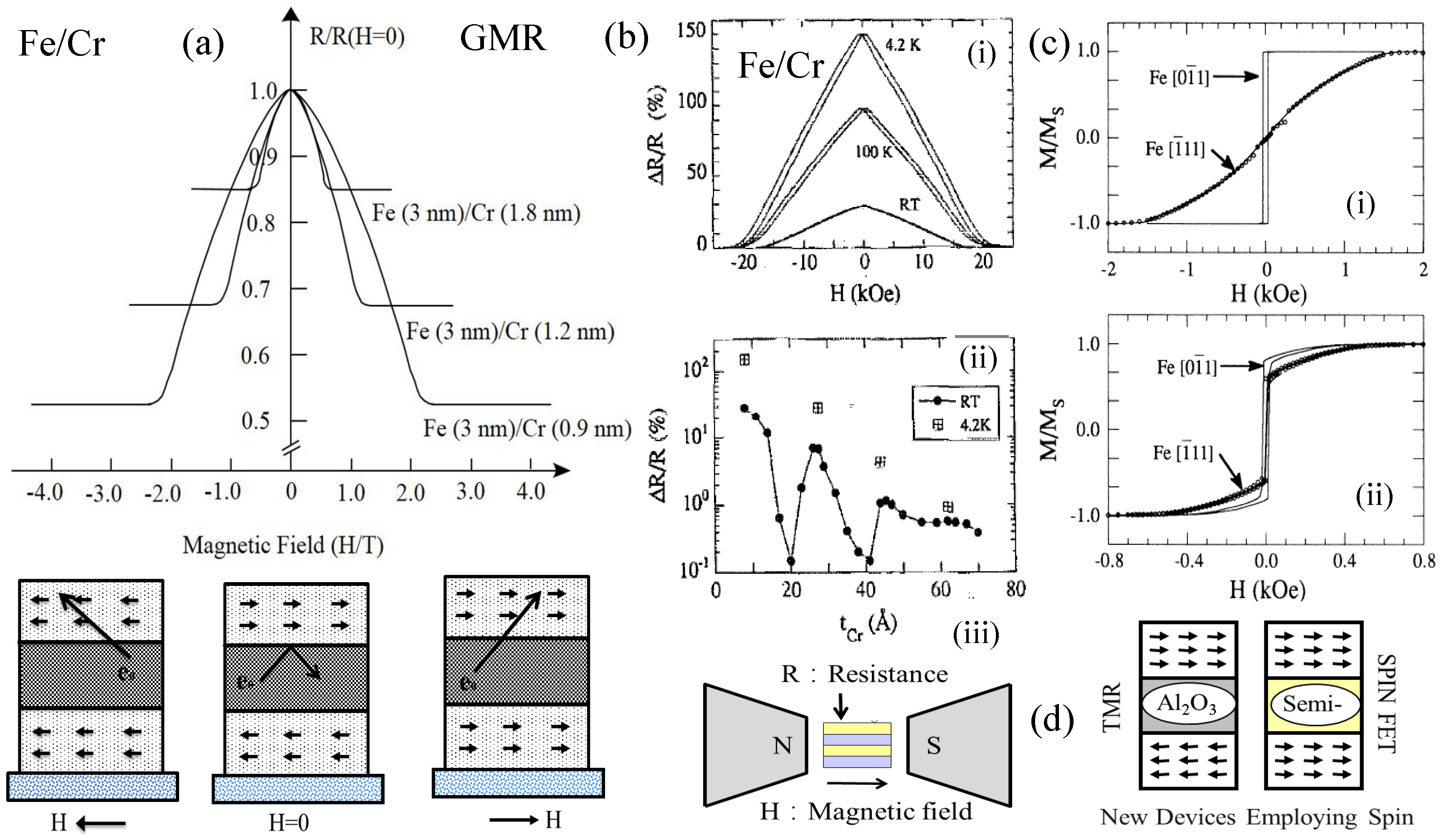
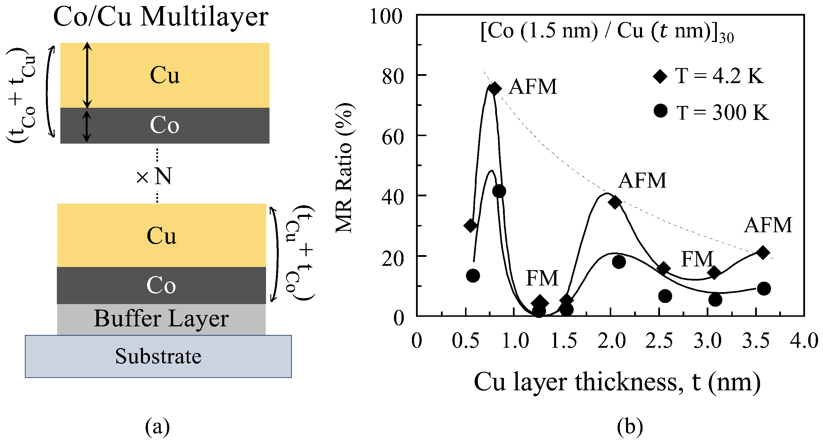
1.1. Giant Magnetoresistance Effect

Essentially, an electrical resistance is called giant magnetoresistance (GMR) when a small externally applied magnetic field, H, can cause a large change in ρ ; usually larger by several orders of magnitude compared to the AMR effect that is normally observed in FM metals and their alloys. Unlike the AMR effect, the GMR effect is a pure quantum mechanical effect, and it is mostly observed in multilayers and alloys of FM material such as Co, Fe, Ni, and NM metals, such as Cu, Ag, Au, including Cr, and these may consist of bilayers and trilayers of FM-NM layers [1,2,34,44]. It is worth noting that the FM and NM layers are grown alternately to a thickness of a few nanometers in total where the thickness of each layer is maintained at the level of few atomic layers per layer. GMR is also observed in metallic multilayers where the thickness of each layer does not exceed a few atomic layers per layer. It has been discovered that the thickness of each NM layer is crucial in defining GMR effect in multilayered structures consisting of FM and NM layers in a repeating order. Particularly, a strong GMR effect is only achieved when the thickness of each NM layer is significantly smaller than the mean free path of conduction electrons—The average length that the electron travels before being scattered is called the mean free path length. However, in some multilayered films, such as those that are very thin, electrons cannot travel the maximum mean free path length; they reach the interface between the two thin layers, rather than being scattered off by another atomic particles or ions. This results in a lower free path for electrons to travel in the very thin material layers. It implies that it is more difficult for conduction electrons to travel through such thin layered films, and the result is higher ρ .
It is a well established fact that the GMR effect in FM multilayer is mainly due to spin-dependent scattering of electrons at each FM-NM interface and in the presence of the applied H field. It implies that a certain threshold number density of conduction electrons need to be scattered at the FM-NM interface in order to achieve a strong GMR effect. The effect was first observed in antiferromagnetically coupled multilayers by Baibich et al. [1] and Grünberg et al. [2], and later by Fullerton et al. [3]. This new discovery of GMR multilayer eventually lead to a shared Nobel prize by Albert Fert and Peter Grünberg in physics in year 2007 [45].
Figure 2 shows a schematic of an experimentally demonstrated GMR effect on a current-in-plane based GMR structure of a Fe/Cr multilayer (a) by Baibich et al. [1] and (b-i,ii) by Fullerton et al. [3]. As shown in this Figure, the normalized resistance decreases with applied H field. In addition, the GMR in these structures periodically changes as a function of Cr layer thickness. Later, Parkin et al., also reported a periodic repeating (oscillatory) GMR effect as the thickness of Cu layers in between Co layers was systematically changed [46]. This is shown in Figure 3. However, the cause of this periodic MR behavior have remained unknown for decades until Ruderman-Kittel-Katsuya-Yoshida (RKKY) proposed their coupling theory [47,48,49,50,51]. Since then, many other FM multilayers were fabricated and scrutinized, including Co/Ru, Fe/Cu, Co/Cu, Co/Au, Co/Ag, and these showed enhanced GMR effects [30,46,52,53,54]. These authors used both the FM/AFM and FM/NM multilayers in current-in-plane (CIP) and current-perpendicular-to-plane (CPP) configurations, whereas glass, Si, and polyimide have been employed as substrates to fabricate multilayered devices/structures.
Puzzling as it may sound, the mystery behind the GMR and MA effects, that arise suddenly, abruptly and instantaneously as soon as a tiny external H field is applied to these FM-NM multilayers, remained unknown for some decades. Even today, we still do not know why and how the externally introduced tiny H field, ϵ , and defects that are inherently generated as a result of it, can cause such a dramatic change in MR and MA in the FM multilayers [55]. Some of our previous studies have shown that the externally applied ϵ , has profound effect on magnetic properties of these kind of FM/NM multilayers and alloys, and in particular, when they are prepared using physical vapor deposition and sputtering techniques [8,40,55,56,57].
Recently we studied the effect of externally applied H and ϵ on the MR and MA properties FM-NM multilayers. We demonstrated that the H and ϵ have significant effects, especially, in inducing MA in Co/Cu [8], Co/Au [58], and Co/Ag multilayers [8,56]. These were produced on polyimide substrates, by varying the FM layer thickness whereas keeping the NM layer thickness constant. These multilayers exhibited strong magnetic anisotropy when the H and ϵ are respectively increased from 0 to 20 kOe and 0 to 1.5% [56,59]. The measured MR along the in-plane parallel to the direction of the easy axis and in-plane perpendicular to the direction of the easy axis showed that the peak of the H dependence of the MR for all these multilayers evidently corresponded to the H c , as demonstrated by M-H curves in [8].
Likewise, e-beam deposited Co/Au multilayers exhibited a remarkable MA when these multilayers were deposited at an oblique angle of 45 ° [34]. Magnetic annealing also seems to have a dramatic effect on these multilayers. A dramatic enhancement in both the MR and MA was observed when these multilayers were annealed at 250 ° C and in the presence of 3 kOe H field. These results suggest that the increase in both MR and MA is related to the change in orientation of magnetic moments from more dis-ordered to significantly ordered states.
Note is to be made that in contrast to those periodic characteristics exhibited by e-beam and chemical vapor deposited films described above, Multilayers prepared using Pulsed-current deposition, did not exhibit any periodic MR characteristics [34,40,46,59]. However, these pulsed current deposited FM-NM multilayers exhibited a remarkable shift in MR peak position favoring smaller Co layer thickness. These experimental results have demonstrated that both the MR and MA properties are sensitive towards Co layer thickness and layer morphology, and these two properties both in combination seemed to play a crucial role in altering both the MA and MR.
Unlike the myriad number of results that have been published so far on FM-NM multilayers which have been fabricated using physical vapor deposition technique, one can find very few reports on FM-NM multilayers that are fabricated using Pulse current deposition technique and it is especially true for reports on Co/Cu, Co/Ag and Co/Au multilayers, fabricated in an atomic scale layer thickness [60].
The room temperature MR effect of Pulsed-current deposited multilayers of Fe/Cr, Co/Cu, Co/Ag, and Co/Au, although small, is achieved at a relatively low externally applied H field. However, a large room-temperature MR effect in combination with high field sensitivity are two important features that are highly desirable in order for any FM-NM multilayers to be useful for practical application. In the presence of an externally applied H field of 10 kOe, the Pulsed-current deposited multilayers of Fe/Cr showed room temperature MR of 8% [61], whereas multilayers of Co/Ag showed a MR of 9.1% [56]. Co/Cu on the other hand showed 4.1% [40] in the presence of 1 kOe and Co/Au showed 4.5% [62] in the presence of 20 kOe. Note is to be made that these results are either comparable to or better than those exhibited by vapor deposited Fe/Cr, Co/Ag, Co/Cu, and Co/Au multilayers. These samples showed a MR sensitivity of as high as 0.02 per unit of Oe.
The sensitivity is estimated as [( R H - R 0 )/ R H )]/ H s where, R H and R 0 are the resistance at H = H and H = 0 fields respectively and H s is the saturating H field. Our magnetic measurements of these multilayers have revealed that even multilayers with strong in-plane magnetic anisotropy saturate at H field well below 100 Oe and the coercive force, H c can be as low as 50 Oe to give saturated anisotropy [7]. All the properties discussed above are highly desirable from the point of view of practical application of FM multilayer as magnetic and magneto-optic sensors.
Recently, metallic multilayers with CPP geometries ranging from that of nanowires to nanopillars have been reported, and this field has become an active field of research due to potential application of FM-NM multilayers in spintronics [6,63]. An interesting feature of the CPP based configuration is that individual layers in these can be made thicker when the current is passed through the interface perpendicularly, and in which case, electron spin undergoes diffusion processes that extend over much larger distances than the electrons mean free path as flipping up of spins in such a case is very rare.
The film preparation for CPP geometries using the existing high vacuum techniques are not as easy as those prepared by making use of CIP geometries. So far, magnetic multilayers have been produced using advanced lithographic techniques to obtain the smallest possible surface area, and to bring the electrical resistance to a more accessible μ m range. However, the technique is not practical because the current density, J, no longer remains uniform throughout the film for even a very small column thicknesses.
Sputtering is another important deposition technique that is being widely used in both academic as well as industrial laboratories for growing multilayers on insulating substrates such as MgO, glasses and plastic, and metallic substrates such as Cu and Au electrodes. As demonstrated by Bao and Kavanagh [63] and several others [64,65], FM metals and FM-NM multilayers have also been produced in the form of nanowires and nanopillars using electro-chemical methods—including galvanostatic electrodeposition and Pulsed-current electro-deposition method [66,67]. Pulsed-current electrochemical deposition techniques, can be used to deposit FM-NM multilayers in a highly confined spaces and the technique allows use of substrates if more complex geometries that are not possible via high vacuum evaporation methods. Besides, Pulsed-current deposition techniques allow fabrication of high quality multilayered films on atomic-scale thickness as well as in the form of granular alloys [34]. These techniques will be discussed in more detail in experimental section.

1.2. Tunnel Magnetoresistance Effect

As demonstrated by Ikeda et al. [10] and Yuasa et al. [68], when a NM layer in a multilayered film is replaced by an insulator such as MgO, the structure thus formed is referred to as magnetic tunnel junctions (MTJs), as these multilayers demonstrate TMR effect. Much in the same way as it is for structures that produce GMR effect, the electrical resistance in these MTJ varies dramatically with the variation of relative direction of M in the FM layer that in turn is responsible for the process of tunneling of conduction electrons through the insulating layer.
While the σ in GMR structures mainly arises from the scattering of conduction electrons at FM-NM interface, in TMR structures it arises from tunneling effect: the electrons tunnel from insulating layer to FM layer to occupy available electron states in the FM layers. The number of tunneling electrons in these configuration is determined by the orientation of M of the electron spin in the adjacent FM layers. For example, the tunneling effect is large when the M of the electron spin in the adjacent FM layers are aligned parallel to the direction of motion of electrons whereas when they align antiparallel, the tunneling effect is small.
Much in the same way as the GMR effect, the TMR effect is a pure quantum mechanical effect as the magnetic movement of the electrons and their spin orientation are conserved before and after the tunneling process. A TMR effect of 14% at 4.2 K was first reported by Julliere et al., for a Fe/GeO/Co configuration [43]. Subsequently, Miyazaki et al. [69] and Moodera et al. [70] reported a MR effect of 18% at room temperature.
Al 2 O 3 , α -Fe 2 O 3 , and MgO are some of the insulating oxide layers that have been incorporated into the FM layers of TMR structures, and with such a modification a highest experimental TMR effect of up to 600% have been reported for MgO modified configuration of thin layered film of FM-NM. Theoretically, a TMR value of up to 1000% has been predicted for this system [71,72].
Half metallic FM electrodes are another group of important thin layered structures that show a strong TMR effect [73]. CrO 2 [74], La 1 x Sr x MnO 3 [75], Fe 3 O 4 [76], and Heusler alloys are good examples of such configurations that show TMR effects of up to 1800% at a temperature of 4.2 K. However, the same configuration showed 90% TMR effect at room temperature. The large MR effect of the TMR structures over the GMR ones is considered to be due to the high spin polarization of conduction electrons at the oxide-FM layer interface.

1.3. Colossal Magnetoresistance Effect

The colossal magnetoresistance (CMR) effect, as the name suggests, is huge, and it is mostly demonstrated by Mn-based perovskite oxides, and it can be of several orders of magnitude higher than that of GMR effect [77]. For example, CMR effect can be up to 3 to 4 orders larger than the TMR effect. However, unlike the GMR and TMR effects, which are observed in FM-NM and FM-Insulator-NM based configurations, respectively, the CMR effect is usually observed in magnetite and perovskites with a general formula of A 1 x B x MnO 3 , where A = (La, Pr, Nd, Sm), where B = (Ca, Sr, Ba) [78,79]. Since magnetite and perovskites are half-metallic ferromagnets, it is assumed that these possess only one spin band crosses the Fermi-level, and as a result they are expected to have a strong CMR effect.
Unlike the physical mechanisms that cause GMR and TMR effects that are well understood, the CMR effect is not yet fully understood. It is believed that this effect is due to the strong competing interactions between magnetic and electronic fields and due to the degrees of freedom for interaction that spins, charges, and orbitals enjoy in manganese oxide layers—leading to exceptionally rich phase transition. More precisely, the effect may have been the result of multiple exchange mechanism involving transition from electronic to magnetic state, interplay between electron-phonon couplings, orbital ordering effects, ferromagnetic to paramagnetic phase transition, and lattice distortions. The CMR effect, which is usually observed in the presence of large H and at a relatively low temperature, however, limits its immediate industrial applications. Nevertheless, as the effect is so large that it can find potential applications in the near future.

1.4. Spin Torque Transfer Effect

Spin-torque transfer (STT) is an other interesting phenomenon demonstrated by layered structures which has already found application in creating non-volatile MRAM memory [80,81,82,83,84]. However, improving MRAM densities with higher speed and greater reliability remains an important challenge in this field [85]. Continuous improvement in design and fabrication methods should in principle help solve this problem and thus overcome their current shortcomings. The same STT phenomena can also be applied to FM/Insulator/FM-based nano-oscillators (STTNOs) as these work at radio frequencies [86]. Although, the STTNOs have been considered to outweigh the performance of the conventional LC oscillators and ring resonators, these still suffer from poor frequency tuning, low power output of less than 1 nW, and large phase noise. Researchers [87] have shown that the precession frequency of spins can be adjusted by changing the magnitude of the applied current, however, it is yet to prove that the spin-transfer induced precession can be used as working principle for making devices with new radio frequency.
Developing technologies for early disease detection, especially in the field of Cancer, which is one of the chief causes of death and possess a serious health risk among people of all ages worldwide, has been a great challenge. Vulnerable human organs to cancer attack are lung, prostate, breast, and colon. These four cancer types account for over 50% of all new fatal cancer cases. It is widely agreed that the survival rate can be greatly improved if the disease is diagnosed in its early stages. Bio-magnetic sensing based on magnetic and spintronic technologies for the early detection of cancer is an emerging field of research [88,89,90]. Technologies based on MR sensors, if successfully developed, can have many merits over other detection techniques such as biomagnetic and magnetoplasmonic sensing. Likewise, magneto-optic properties in FM multilayers has been known for decades, but it is only recently a noticeable research interest has been seen in this subject, and it is especially true when we talk about bio-magnetic sensing for early disease detection. These, for example, offer high sensitivity and easy integration with electronics and microfluidics, while being cost effective and portable.
While there are several reviews that discuss the GMR, GMRE, and MA effects shown by FM multilayers, only a few reports are available on shortcomings of physical properties of multilayered films such as weak MA at a relatively small applied H field of less than 50 Oe, low sensitivity to H field, small saturation magnetization, M, and on how these shortcomings can be overcome. It is generally acknowledged that understanding of electronic, magnetic, chemical, and optical properties of these multilayered films and the relationship between layer texture such as layer thickness, roughness, and composition need a close and rigorous scrutiny, as these properties are crucial in manipulation and optimizing behavior of these material.
This review aims to address these aspects as well as potential technological applications and future prospects of multilayered thin films of periodically repeating FM-NM structures—including those produced by pulse current deposition. Since questions such as how multilayered thin film configuration consisting of FM-NM respond to externally induced ϵ and how such ϵ produce defects in these systems and how these defects would have such a profound impact on MR and MA phenomena exhibited by these structures are still not fully understood. It is for these very reasons, this area still demands further research and development work. This review also aims to discuss MR and MA properties displayed by obliquely-engineered multilayers as well, and a special attention shall be given to application of strain-induced magnetic effects such as MR, MA, MO effects—including the nature and origin of MR, mechanism associated with spin-dependent σ and artificial generation of MA. The review concludes with a brief discussion on giant magneto-reflectance effect, GMRE, and magnetoplasmonic based next-generation sensors of multilayered thin films of dielectric, magnetic, and non-magnetic metals.

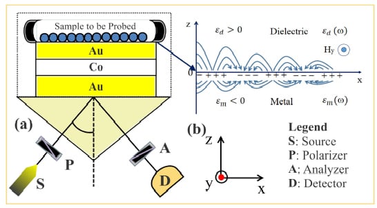
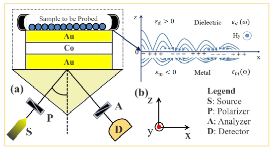
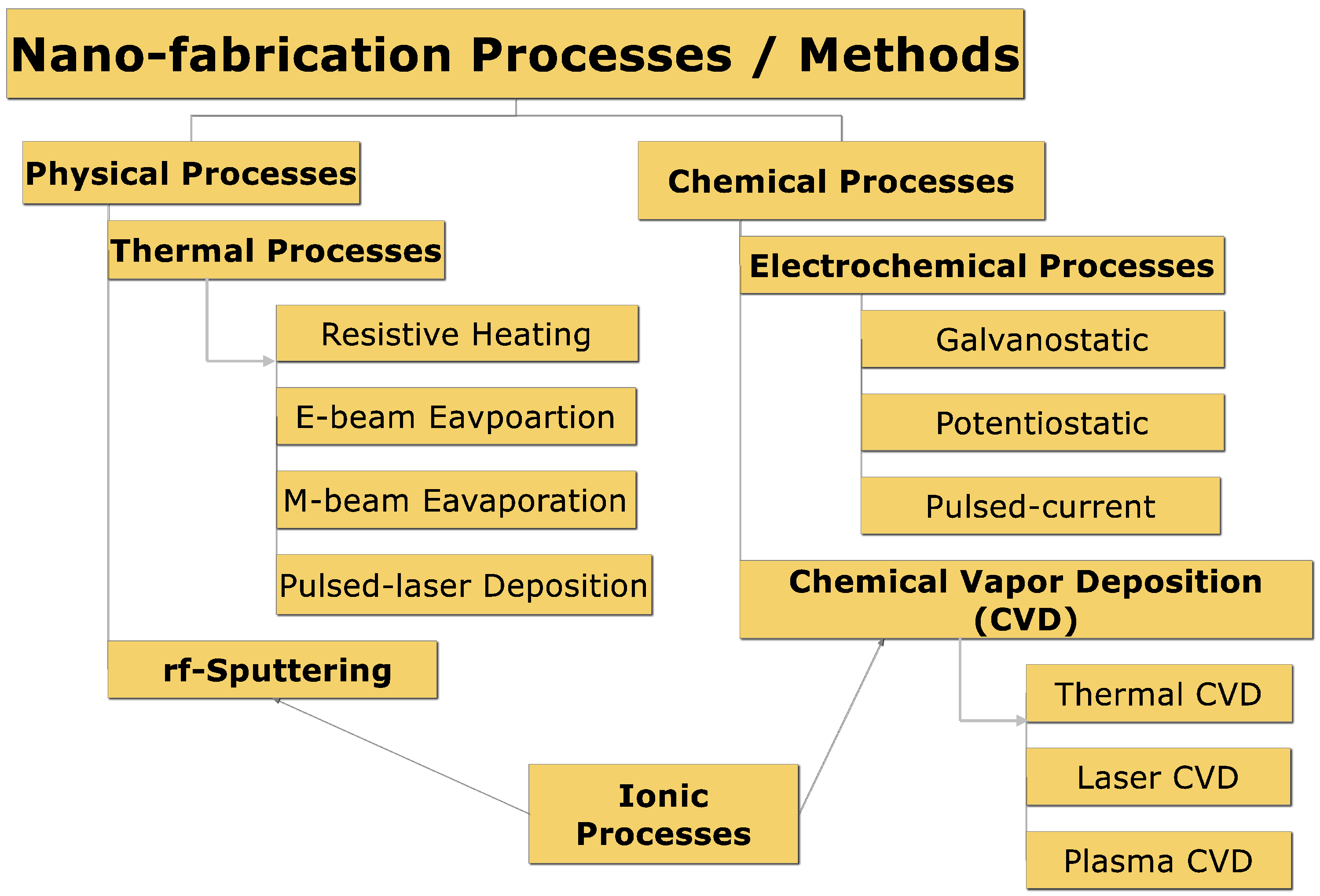
2. Experimental Methods

As shown in Figure 4, a wide range of synthesis methods are used to produce multilayers consisting of FM layers based on periodically repeating order, and these range from physical processes such as, thermal and sputtering methods, chemical processes such as electrochemical and chemical vapor deposition techniques to non-equilibrium techniques such as Melt-spun and mechanical alloying [91].
Thermal processes are further subdivided into thermal heating methods, electron-beam evaporation, pulsed-laser deposition (PLD), and molecular-beam evaporation (MBE). FM multilayers can be deposited using simple thermal heating as well as more sophisticated vacuum based techniques such as, molecular beam epitaxy (MBE), e-beam evaporation, and pulsed laser deposition methods. Thermal heating involves resistive heating of source material, usually metal, and this requires using of the metal as a resistive filament which gets evaporated when heated at pressures below 1 × 10 6 Torr. Molecular beam epitexy, MBE, is a slow deposition process that requires ultra-high vacuum of below 1 × 10 11 Torr., at all times. E-beam evaporation is principally similar to MBE method except it is simpler to operate. The pulsed-laser deposition technique is usually being used to grow multilayers with oxide layer.
The Oblique incidence e-beam evaporation technique is one of the preferred methods for controlling magnetic properties of micro to nano-sized multilayered films. Recent work on FM multilayers have shown that obliquely deposited multilayers exhibit strong magnetic anisotropy and the magnitude of the anisotropy enhances when samples are annealed in the presence of H field [4,19,92,93,94]. Since these multilayers are deposited onto the substrate by changing deposition angle, this technique help break structural symmetry with respect to multilayer plane, producing tilted columns, shadowing effects and voids in the directions parallel to the plane of evaporation: The deposited particles can also form chains of crystallites, leaving behind some voids, and these voids lead to an array of fine crystals that extend in the direction perpendicular to the direction of the incidence beam [20,24,30,95].
The easy axis of magnetization may form along the direction of these crystalline chains, which is perpendicular to the incident plane of evaporation. Experimental evidences have shown that the FM multilayers exhibit strong room temperature magnetic anisotropy in the presence of a tiny magnetic field and magnetic annealing was found to enhance this magnetic anisotropy significantly [21,22,34,96]. For the obliquely deposited multilayers, the strength of anisotropic effect is found to be directly correlated with the angle of deposition.
The non-equilibrium pulse laser deposition (PLD) method is an improved thermal process and this method is suitable for depositing alloys and oxide films with controlled chemical composition.
Sputtering deposition is an ionic process and it is widely used for making multilayered films in magnetic industry, and it is a non thermal electrical process. Traditionally, this technique has been widely used for the deposition of planner multilayers, however, recently, it is also employed to produce nanowires and nanopillars shaped multilayered structures. The uniqueness of this technique is that it permits almost any combination of elements to be deposited and has been useful for depositing metals of high melting point.
Chemical processes range from simple chemical deposition method to more advance constant current galvanostatic, potentiostatic, and potentiodynamic to Pulsed-current electrodeposition techniques to chemical vapor deposition methods such as Plasma, Laser and Thermal vapor deposition [5,32,34,60,63,97,98,99,100,101,102,103,104,105,106,107,108,109,110,111].
Chemical deposition techniques, such as, spraying and spin coating techniques are extensively used in industry. Except electrochemical techniques, other Chemical techniques suffer from the following major draw backs—including impossibility of precise control over film thickness and making of miniature devices of nano and micron size dimension of multilayered film [66]. However, these are easy to use and inexpensive room temperature based techniques. As deposition of metal is aimed at making multilayered thin film structures of nano and micro dimensions of controlled thickness, these chemical techniques are not practical for this purpose.
Constant current electrochemical techniques such as galvanostatic, constant potential techniques such as potentio-static and potentio-dynamic, also referred to as cyclic voltammetry, and Pulsed-current techniques are more advance and sophisticated room temperature based deposition systems that allow more precise control over deposition parameters such as film dimension and layer thickness by having precise control over solution concentration, deposition current density or potential and pulse height [67].
The limitation is choice of substrates—as all electrochemical techniques need metallic substrates or electrodes with good σ so as to be able to deposit any metallic thin film. Recent advancement in electronics and automation technology, however, has made these techniques so advanced and sophisticated that a well trained experimentalist can deposit metallic film of atomic scale thickness using these techniques. In addition, as each metal possess its own deposition potential or current density at which it can be deposited, these techniques allow deposition of one metallic layer over another producing multilayered films.
In the past few decades, the electronics industry has benefited tremendously from the numerous innovations in Pulsed-current techniques [67]. In particular, in thin film industries, the quality of the film is determined by the efficiency and cost effectiveness of the deposition techniques. For example, for any given application, depending on cost of deposition and specific need for a substrate, one can choose to apply a right deposition method. Choice of deposition techniques is assessed depending upon the specification of the final product—including type of metal to be deposited, film dimension, required numbers of layers, type of metal in each layers, etc. Using this technique, the dimension, composition, and thickness of the film layer can be precisely controlled by having control over deposition parameters such as solution composition and concentration, magnitude of deposition current density and applied potential, deposition rate and pulse width. The various possible parameters used for the fabrication of the Co/Cu, Co/Au and Co/Ag multilayers are listed in Table 1.
Pulsed-current deposition method have been used by us and several others to deposit multilayered structures of nano-dimension of Co-Cu, Co-Au and Co-Ag and the typical deposition conditions used are respectively outlined in [60,97,105,107,112,113,114,115] and [64,67,103]. Other non-equilibrium processes, such as melt-spun [116,117] can be used to prepare long ductile ribbons whereas mechanical alloying [118] can be chosen to engineer granular alloys; their use, however, is mostly limited to making bulk films.

3. Theoretical Models

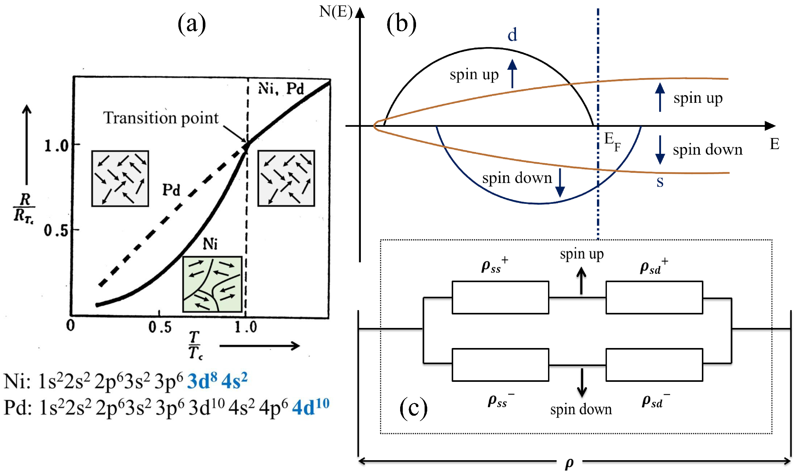
3.1. Electrical Conduction in Metals

Conductivity, σ , in metals and multilayer structures is explained using electron spin-dependent two current model. However, before proceeding with spin dependent σ model, it is important to understand how the electrical resistivity, ρ , of group 10 metals such as, 3-d transition metals (Ni, Pd, and Pt) and their alloys with Group 11 metals such as Cu, Ag, and Au fluctuates with temperature. It has been demonstrated that the effective number of conduction electrons of Group 10 metals is almost the same as the effective number of conduction electrons of Group 11 metals. However, the mean free path of conduction electrons of Group 10 metals is believed to be insignificantly smaller (≈ 1 nm) as opposed to mean free path of conduction electrons of Group 11 metals. It means, under small lattice vibrations, the 4-s conduction electrons of the group 10 metals, can easily make transitions to unoccupied 3-d states. The probability of these transitions is several times greater than the probability of scattering of 4-s electrons in Group 11 metals. Since 3-d electrons are responsible for ferromagnetism in 3-d transition FM metals, it is believed that there exists a direct relationship between ρ and magnetism shown by these. Subsequent sections describe origin and mechanism of σ in FM metals first and then spin-dependent σ in FM multilayers.
Figure 5a shows experimental results of the normalized electrical resistance ( R / R T C ) versus normalized temperature ( T / T C ) curve for ferromagnetic Ni and nonmagnetic Pd, both being Group 10 transition elements [42]. R T C is the electrical resistance at the Curie temperature, T C (670 K) of Ni. As shown in the Figure, the electrical resistance of ferromagnetic Ni below 670 K is always smaller than that of Pd. As shown by the vertifical dotted line, at 670 K Ni experiences its ferromagnetic order-disorder transition, whereas Pd does not. Above 670 K, the ρ curves of both the metals follow the same path. This kind of transition of electrical resistance at 670 K is believed to arise from the magnetic spin states of ferromagnetic Ni, whereas in Pd the spin states are unaffected by the variation of temperature.
Electrical conductivity, σ , of FM metals differs from that of diamagnetic metals (DM) and paramagnetic (PM) materials. FM material such as Fe, Co, and Ni show a large positive magnetic susceptibility, χ in response to externally applied H fields, whereas PM material such as Al, Li, etc., show a small positive χ and induced H field acting along the direction of externally applied H field. Al, Mn 3 + , and salts of Ni and Fe are a few good examples of material that show good PM characteristics, primarily due to incomplete inner electron shells that they possess. On the other hand, DM metals such as Au and Ag, including compounds such as H 2 O, etc., show relative magnetic permeability, μ r 1, and therefore χ 0, and the induced H field opposes the externally applied H fields.
The large σ shown by FM metals as compared to PM and DM metals can be explained using the schematics of Figure 5b: the density of occupied states (DOS)—number of states per unit volume, N(E), at the Fermi energy, F E , level of the 4-s and 3-d transition metals are split into spin-up and spin-down energy bands. Since the splitting of 4-s bands at the F E level is symmetric, the 4-s scattering has almost no effect on N(E), and it can be neglected. The shifting of 3-d down-band is due to the exchange interaction and is usually in the range of 1 eV to 2 eV. While the N(E) of the 3-d spin-up electrons is completely filled and lies below F E , the N(E) of the 3-d spin-down electrons is only partially filled up, and extends beyond F E level. As a result, the spin-down electrons, as compared to the spin-up electrons, are more prone to scattering due to the available empty space between the spin down 4-s and 3-d bands.
Note that the ρ due to the 4-s and 3-d interaction is much larger than the ρ due to 4-s and 4-s interactions. On the other hand, as the N(E) of the 3-d spin up (↑) electrons is completely filled up, the 4-s spin up (↑) electrons can only scatter to other 4-s spins up (↑) states as there is no room for interaction within the 3-d spin-up (↑) electrons. This is the reason why the ρ caused by s-d interaction shown in, spin-down (↓) band in Figure 5b, is much larger than that of the interaction between s-s electrons: The notation s-s stands for the interaction that takes place between the 4-s conduction electrons whereas the notation s-d stands for the interaction between the 4-s conduction and 3-d electrons.

3.1.1. Mott’s Two-Current Model Applied to Metals

Figure 5c shows Mott’s two-current model applied to FM metals. This model is based on three assumptions: (i) That spin number is conserved—spin of the charge carrier is preserved, i.e., One can not expect any changes in spin orientation due to scattering; (ii) that the s-electrons are almost exclusively responsible for conduction; and (iii) that the ρ that arises due to the scattering of spin-up (↑) 4-s and spin-up (↑) 3-d electrons, and spin down (↓) 4-s and spin down (↓) 3-d electrons can be added.
As described earlier in Figure 5b, the available empty space in the DOS of the 3-d spin-down (↓) electrons is much bigger than that of the 4-s spin-down (↓) electrons, the ρ in the lower branch is mainly due to the interactions between the spin-down (↓) 4-s and spin-down (↓) 3-d electrons whereas the ρ in the upper branch is mostly due to the interactions between the spin-up (↑) 4-s electrons themselves. Note that the symmetry of the DOS of the s-electrons implies that ρ s s = ρ s s + . After simplification, the equivalent ρ of the FM material is the parallel combination of the resistivities associated with the spin down ( ρ = ρ s s + ρ s d ) and spin up ( ρ + = ρ s s + + ρ s d + ) electrons, and ρ is given by ρ ρ + / ( ρ + ρ + ) .

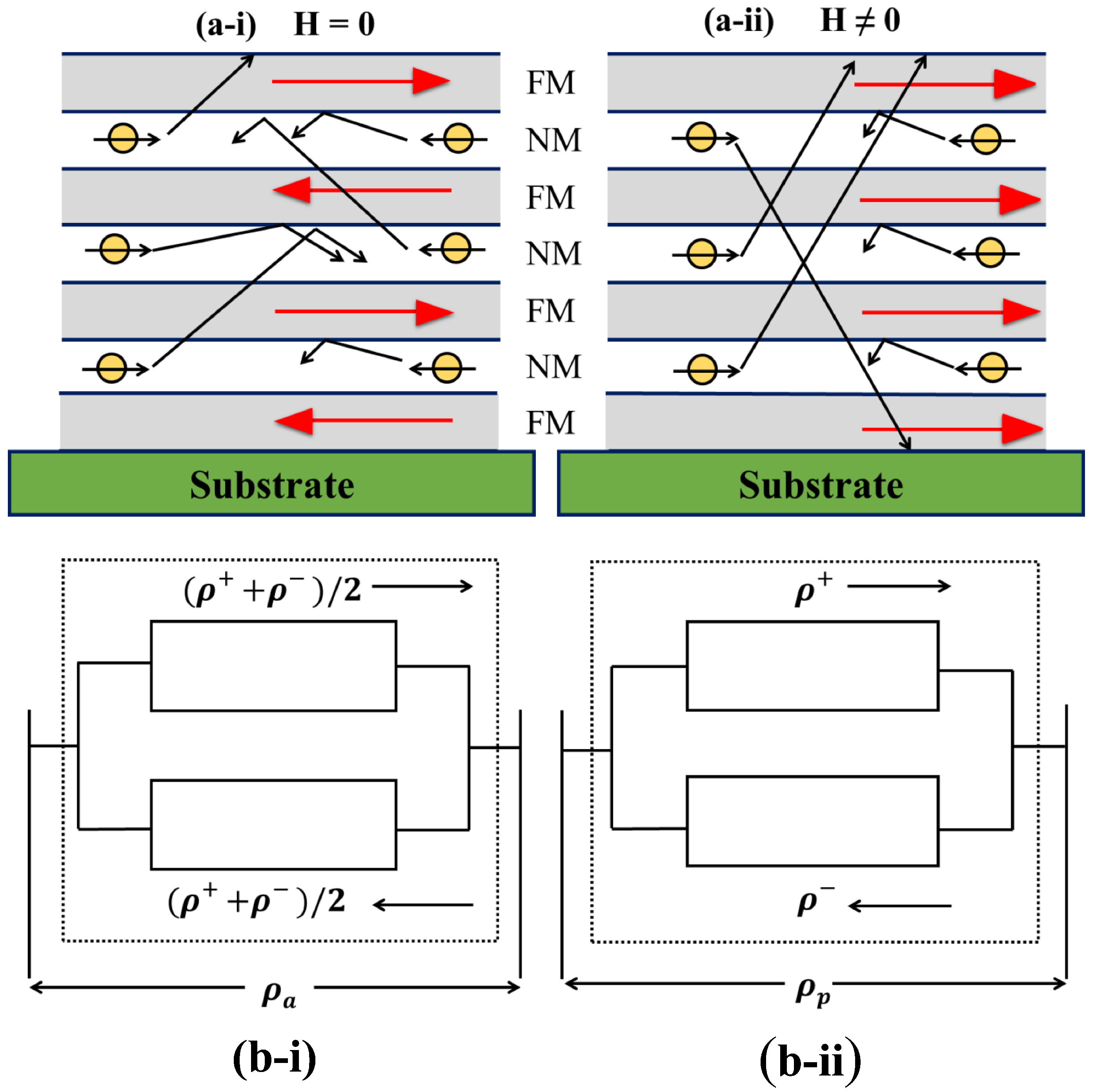
3.2. Electrical Conduction in Multilayers

Transport models such as Classical and semi-classical, quantum mechanical, RKKY coupling, and Kondo effect, have been proposed to account for the spin-dependent scattering at FM-NM interface [119]. Camley and Barnaś first proposed a classical model on GMR effect in FM multilayers for CIP geometry [120,121]. They used Boltzmann’s transport equation to explain spin-dependent scattering process at the FM-NM interface of FM multilayers. This model suggests that the magnitude of the GMR effect depends on the ratio of the FM layer thickness and mean free path of the conduction electrons, and the scattering asymmetries of spin-up (↑) and spin-down (↓) electrons. On subsequent reports these authors considered, in addition to the scattering at the interface, bulk scattering. They showed that the primary cause of the GMR effect in CIP-based geometries can be accounted for the diffusive scattering at FM-AMF interface as well as for spin-dependent scattering at the FM-NM interface.
In subsequent years, for CPP based geometry, Valet and Fert proposed a semi-classical model, based on free electron approach of Boltzmann [122]. It is essentially similar to the one proposed by Camley and Barnaś [121]. The difference between these two models lies in the fact that the latter provided a means to separate volume and surface contributions to spin-dependent scattering and magnetic anisotropy phenomenon. Both of these models, however, do not account for any electronic structure of the metals in question. More importantly, these models cannot explain the quantum effect that arises when the layer thickness approaches mean free path of the conduction electrons.
Levy et al., proposed a free-electron quantum model using Kubo’s linear response formalism [123]. This theory was later extended by Camblong et al. [124] by avoiding local approximation for the σ effect and neglecting both the quantum interference and size effects. The approach was further extended to account for spin-valve structures and the bulk spin-dependent scattering effects. As far as we know, no single complete model is available to date to describe conduction mechanism that prevails in periodically structured multilayered FM-NM based films.
Asano et al., proposed a new model by taking into account of localized atomic orbitals, which may arise under the single-band-tight-bonding condition, to describe electronic structures of the metals used [125]. The model was extended by Itoh et al., who took into account the origin of the GMR effect in both CIP and CPP configurations [126]. In their extended model they took account of both the single-band-tight-bonding method and the single-cell coherent potential approximation method to explain their theory on ρ that arises on FM multilayers as a result of electron scattering effect. Subsequently, Todorov et al., used real-space Green function to describe the σ that arises as a result of both the free-electron and quantum effects, and this is applicable to both the metallic alloys and multilayered structures [127]. Models offering a more complete picture, such as multi-band tight binding models were proposed by Schep et al., to account for both these and scattering matrix as well as d-band DOS of FM metals [128]. These models were essentially found to be more accurate in explaining process such as oscillation of MR with layer thickness and as a matter of fact the multi-band models give a more clearer picture of the MR effect in metals and multilayers. These models accounts for over-lapping of s-p and 3-d bands as the dimension of film layer approaches electron’s mean free path.
Using the band theory and taking into account of the semi-classical theory, Oguchi et al., proposed a constant relaxation approximation method [129], which was extended by Binder et al. [130] and Butler et al. [131] to include roles of both the interfaces and impurities. The impact of defects and ϵ on MR is still difficult to understand, so is the case with quantifying them and with developing a control mechanism. Tsymbal et al., attempted to incorporate the effects of defects, voids and lattice distortions into the band theory and the quantum mechanical effect arising as a result of these [132].
Buttler et al. [131] used first principle model to account for electronic structure and quantum mechanical formalism to describe the MR contribution from both charge and spin transfer at FM-NM layer interface. This model was expanded by Blass et al., who added spin-orbit coupling effect and this model successfully accounted for the MR effect arising from both the electronic structure and spin-dependent scattering at the FM-NM interface due to defects and impurities [133]. Although none of the models have been able to describe the complete mechanism of MR effects in multilayered films, the two-current model proposed for metals in Section 3.1.1, still forms a strong basis for quantifying MR effect in magnetic multilayers.
The mechanism responsible for the GMR effect in multilayer is considered to be different from the mechanism responsible for the AMR or OMR effects in metals. It is generally believed that the AMR effect primarily arises from the bulk scattering, i.e., spin-dependent scattering within the layers. On the other hand, the GMR effect primarily arises from the spin-dependent scattering of electrons at the FM-NM interface, and it occurs when the thickness of the NM layer is smaller than the spin-diffusion length. The scattering probability of the conduction electrons in this case, largely depends on the relationship between the orientation of spin of the 4-s conduction electrons in the NM layer and the direction of magnetic spin of the 3-d electrons in the FM layers.

Mott’s Two-Current Model Applied to Multilayers

Figure 6a shows a cross-sectional view of a multilayer, consisting of alternating layers of FM and NM. The direction of the magnetic moments of 3-d electrons in FM (red arrows with large heads) and the 4-s conduction electrons in NM (small black arrows with circles) are labeled with the corresponding arrows. The long black arrows across FM and NM layers are connected to show scattering paths of the s electrons, and when H = 0, as is the case in Figure 6a-i. As shown in this Figure, magnetic moments in the adjacent FM layers are aligned antiparallel. In this situation, those 4-s conduction electrons of NM that are aligned parallel to the magnetic spins of the 3-d electrons of the FM, can easily pass through the first FM layer without any scattering effect. However, as they encounter the second FM layer with magnetic spins of the 3-d electrons that are aligned antiparallel to their own spin direction, they get scattered. It seems that the spin orientation of the 4-s conduction electrons does not change after scattering. The movement of both the spin-up (↑) and spin-down (↑) conduction electrons is, therefore, repeatedly interrupted by multiple scattering processes, leading to noticeably high ρ in these multilayers.
The ρ caused by scattering of electrons at the FM-NM interface can be significantly reduced by applying H field that helps overcome anti-ferromagnetic coupling interaction of 3-d spins, leading to parallel alignment of 3-d spins in the adjacent layers. This H field forces the magnetic spins of the 3-d conduction electrons of the FM layers to align in the same direction as the direction of applied H field. In this situation, while 4-s conduction electrons with spin-up (↑) and parallel to the magnetic spin of the 3-d electrons would freely pass through the FM layer without scattering, the 4-s conduction electrons with spin-down (↓) and anti-parallel to the magnetic spins of 3-d electrons would undergo multiple scattering in each layer as they travel from one layer to another. In the case, the movement of the spin-down (↓) 4-s conduction electrons is, therefore, repeatedly interrupted by multiple scattering processes, while the spin-up (↑) 4-s electrons can pass freely through the FM layer without interruption, and this leads to a noticeably low ρ of the multilayer. The decrease in ρ is up to 2 orders of magnitude.
Figure 6b represents Mott’s two-current model as applied to multilayers. In this case, when the magnetic moments in the adjacent FM layers are (i) antiparallel (i.e., H = 0 case) and (b) parallel (i.e., H ≠ 0 case): (i) shows the ρ arising from the spin-up (↑) and spin-down (↓) electrons of FM layers (and thus the current), when the magnetic spins of the 3-d electrons in the adjacent FM layers are aligned anti-parallel to each other and (b) shows the same situation but when the magnetic spins of the 3-d electrons of the adjacent FM layers are aligned in parallel to each other.
Changes in ρ due to the applied H field can be given as, Δ ρ / ρ p = ( ρ a ρ p ) / ρ p , where ρ a is the electrical resistivity in the absence of H field, and it is obtained from the parallel combinations of the resistivities as shown in Figure 6b-i. ρ p is the electrical resistivity in the presence of an externally applied H fields, and it is obtained from parallel combinations of the resistivities as shown in Figure 6b-ii. After simplification, the relative change in ρ due to applied H fields is given as [134], Δ ρ / ρ p = ( 1 α ) 2 / 4 α , where α is the scattering asymmetry parameter, and it is given by ρ / ρ + . The magnitude of the GMR effect thus depends on the difference between ρ and ρ + , i.e., the difference between the spin down (↓) and the spin up (↑) electrons.
Note to be made that most reviews on spin-dependent σ exhibited by FM multilayers have been examined by looking into the spin arrangement along the cross-section of the multilayer structures. To better understand spin-dependent scattering in FM multilayers and the conducitivity mechanism associated with them, in addition to studying spin arrangement along the cross-section of the multilayer, it is important to study domain formation and spin arrangement along the surface of the film. Moreover, as noted above, the following two conditions must be satisfied in order to achieve a large GMR effect : The thickness of the FM layers must be in the nanometer scale and the thickness of the NM layer must always be less than the mean free path of the conduction electrons. However, this is not always the case for the bulk material.
Figure 7 shows schematic of nano-structured FM/NM multilayered films, in this case trilayers, showing various magnetic domains and orientation of magnetic spins at the interface, along the surface of the FM layers: (a) isotropic (H = 0) and (b) anisotropic (H ≠ 0). A new method is required to change the orientationof magnetic spins the nanostructrued multilayered films from a random orientation to an uniaxial orientation. This method deserves further analysis and is left out for future review.
It is important to point out that the models for conduction in multilayers presented in Figure 5 through Figure 7 respectively are meant to show the state of the ρ / σ profile for both the metals and multilayers, and this forms the basis for all layered structures. Essentially, this model can also be applied to spin-valve (SV) structures—including configurations having multiple layers of varying sizes and dimensions. The conduction mechanism of SV structures is similar to that of the multilayers, save the direction of M of one of the layers is fixed in SV in one direction. It is usually acheived using an antiferromagnetic layer. Since the M of this layer points in one direction, the rotation of the magnetic spins in free layer “opens” when in parallel configuration and “closes” when in anti-parallel configuration with respect to the direction of flow of electrons, which is the origin of the name spin-valve. Interested readers are suggested to read paper by Butler et al. [131], Locatali et al. [6] and online resources available elsewhere.

4. Potential Applications

As opposed to many other scientific investigations that are still at their fundamental research stage, the GMR-based sensors have already made it to the applied arena and market place [135]. The most prominent use is being in making magnetic read head sensors. IBM introduced the first hard drive with a GMR read head in 1997 [136,137]. The time between the discovery of GMR and its first commercial read head sensors spanned only nine years, which is a relatively short time period compared to many other fields. This rapid time to market was due to the use of previously gained knowledge associated with the development of AMR and Hall based sensors. Since the discovery of the GMR phenomena and its application to magnetic read head sensing, there has been dramatic improvements in the storage density of hard disk drives.
Recently, GMR sensors have found new area of application in biology and medicine. GMR based sensors can also be employed especially for target delivery of drug molecules and detecting action potential generated by neuron cells [138]. For example, GMR sensors have been used to detect H fields generated by action potentials propagating along the axon of a neuron. GMR sensors have also been employed in magneto-cardiography (MCG) and magneto-encephalography (MEG) [139], where the H fields produced by heart and brain cells are recorded, respectively. GMR sensors are particularly well suited for biomagnetic applications due to their small size, low fabrication cost, portability, and low-field detection range.
Magnetic sensors have also been used for medical diagnostics to detect proteins and nucleic acids that are labeled with Ferromagnetic particles. The first use of magnetic sensors to detect biomarkers labeled with magnetic tags was reported in the literature in year 1997 [140]. These researchers used a superconducting quantum interference device (SQUID) to detect binding of antibodies labeled with magnetic tags. While successful, the operating conditions required liquid helium cooling and a magnetically shielded room, and these in combination limit practical application of SQUID-based biosensors [79,89,141,142,143,144,145,146,147,148,149,150,151,152,153].
In year 1998, Baselt et al., demonstrated detection of biomarkers labeled with magnetic tags using GMR sensors [141]. These GMR sensors have the advantage of being able to operate at room temperature with ease, making them more attractive, particularly for portable applications.
GMR based sensors can also be employed in magneto-immunoassay (MIA). An illustration of a MIA is given in Figure 8a. As shown in that Figure, the magnetic sensor is functionalized with a capture antibody that is highly specific to a particular protein biomarker. Once captured, a detection antibody conjugated with a magnetic label, often a nanoparticle of 10–100 nm, binds to the biomarker. The stray H fields from the magnetic nano-particle is quantitatively detected using an underlying magnetic sensor.
Arrays of GMR sensors, such as the one shown in Figure 8b, can be used to screen multiple biomarkers where each sensor is functionalized with a different capture antibody [154]. DNA can be detected in a similar fashion by substituting the antibodies with single stranded nucleic acids. One of the most compelling reasons to use magnetic sensors compared to conventional optical techniques, such as UV-VIS and IR spectroscopies, is based on the idea that the biological samples such as bio-fluids intrinsically lack background signal, which leads to a very low limit of detection. For a more comprehensive review of magnetic biosensing, the reader is referred to the body of the research papers available online. However, for GMR sensors to be useful in biology and medicine, the sensitivity of the GMR structures still needs to be improved over 10% per applied H fields of 10 Oe or less, which is a challenging task at the present time.
Another application of GMR sensors is in industrial control and automation, particularly for making position detection using a GPS type mechanism [155]. In this case, permanent magnetization patterns are affixed to the object to be tracked. The GMR sensors sense or detect the changes in the H fields as a result of displacement of the object. Additionally, GMR sensors are used for measuring rotational speed of motor and engines and for angular position sensing. The market for these sensors is driven largely by the growth in automobile industry and in other fields. The GMR based sensors have already replaced many of the AMR sensors previously used in this sector. For a detailed review on recent developments of MR sensors in industry, readers are referred to paper by Jogschies et al. [156] and Van den Berg et al. [157].
Due to their miniature size, high-speed detection ability, and high degree of sensitivity, GMR sensors are also being used in robotics and are expanding into sensing electrical current in industrial applications, including in electronic industry for monitoring current in integrated circuit and electrical isolators. In civil engineering, GMR sensors are used for the detection of Earth’s H field as well as perturbations in the H fields produced by ferrous bodies. Aerospace is another area where GMR sensors may shine. GMR sensors can also be applied to quantum configurable logic devices, such as the programmable logic gates.
Another important application of GMR sensors is in non-destructive testing and evaluation studies. Interested readers are referred to papers by Jander et al. [158], and Tian and his research groups [159,160,161]. For information on high spatial resolution, magnetic field induced thermal imaging techniques, interested readers are referred to paper by Cui et al. [162].
Other areas where GMR sensors can find potential applications are traffic speed monitoring and for measuring very high H field such as magnetic levitation. In addition, electrodeposited nanowire based GMR sensors have been considered as potential candidates for acoustic sensing [163]. Similarly, a room temperature GMR in organic system may find applications in the near future. So far these material have displayed only up to 40% GMR effects at low temperature [164].
The application of spin transfer torque (STT)-based on magnetic nanopillars, is extending to the high-speed, high-density magnetic random access memories (MRAM). Two types of switching mechanism have been proposed for STT based devices. One is the magnetic field-driven magnetization method and the other is the current-driven magnetization method. The former demands a large H field whereas the latter requires a precise control of the field time. A practical current driven magnetic switching method is one area, which is currently being explored at Choi’s laboratory [165,166]. Choi and his collaborators have theoretically demonstrated vortex chirality switching in FM pillars, providing a novel means to controllably switching the vortex chirality in nano-scaled magnetic pillars. The proof-of-concept experimentally has been demonstrated recently by Albert Fert’s group [6].
As shown in Figure 9, so far 64 MBits STT-MRAM using common dynamic RAM interface has been demonstrated by Everspin, and they used 90 nm node technology to achieve the result [80,81]. The STT-MRAM is a low energy density, compact, and cost-effective alternative to earlier version of MRAM. However, higher power consumption and low output power, are still a challenge for these devices. In the case of MTJ based MRAM technologies, bit flipping is done by passing a current through the MTJ structure. The applied voltage draws current through a reference layer. Electrons that tunnel through the barrier layer trigger the torque of the spins of the free layer and magnetize. The process can be controlled by sweeping the voltage from a negative to a positive value, and vice versa. The resistance of the structure is described by MR phenomena that was discussed earlier.
A magnetic tunnel junction-based STT device, similar to the one proposed by Katine et al. [167] and Courtland [168] carries significant promise for making non-volatile MRAM devices. Besides non-volatility, they possess other important features such as high speed and reliability—characteristics that are most essential for new generation of information storing devices. In addition, for the MTJ based MRAM, the array of memory cells, with each cell consisting of one MTJ junction, as compared to six transistors employed by previous generation of static RAM, significantly improving manufacturing capabilities.
The spin-dependent conductivity, σ , phenomenon together with the magnetization, M, switching in FM nanopillars have been considered for various physical implementations of nanomagnets—including radio frequency oscillator such as the STT Nano oscillator (STTNO) [87].
The STTNOs, however, still suffer from poor frequency tuning, low output power of less than 1 nW, and large noise to signal ratio. To overcome various limitations of STTNO, Anna et al. [169] earlier proposed using arrays of phase-locked metallic oscillators in MgO based MTJ structures that provides higher power output in the micro-watt range. As shown in Figure 10a, the device consists of CoFe/Ru/CoFe MTJ based typical configuration. Since the electrical resistance of the MTJ is largely dominated by insulating barrier layer, it is possible to control electrical σ of the MTJ stacks by choosing an appropriate thickness and diameter of the barriers, and making it compatible with the CMOS technology. Figure 10b shows a differential magnetoresistance plotted against applied H field.
Digital control of the bias current reduces the phase noise by improving the impulse sensitivity function and minimizing the step frequency, resulting in high resolution. Additionally, the STTNO is considered to have a very high quality factor. Given their compact size, scalability and simple architectures, STTNOs are expected to reduce the fabrication cost and increase yield, in both the wired and wireless communications, a low cost, low phase noise, higher power output, and high resolution devices. A wide range of features and functionalities of STT Nano-oscillator are shown in Figure 10c.
MgO-based MTJ structures constitute an excellent alternative to GMR nanopillars due to their larger MR effects of over one order of magnitude and ease of control of output power using a voltage bias for oscillator applications. Phase-locking of more than two devices is still, however, challenging and the technique has not yet been proven. A quantitative study of STT driven dynamics in MgO-MTJs is yet to be done, and mechanisms of spin-momentum transfer in TMR structures are yet to be investigated.
Ferromagnetic multilayer based H field enhanced sensing, which makes use of propagating surface plasmon polaritons (SPP) in ferromagnetic layer structures and magnetic field, is relatively a new field of science. SPPs are electromagnetic waves that propagate along the interface between metal-dielectric or metal-air media. These systems show significant future promises, especially, in fulfilling the demand for ultra-fast sensing and detection, higher signal-to-noise ratio (SNR) sensing, and miniature devices, which are needed in monitoring biological and chemical changes taking place in solutions with extremely low protein concentration [11,12,13,14,15,16,18,170,171]. This magnetic field enhanced sensing utilizes Surface plasmon resonance (SPR) in the presence of H field, which is the optical excitation of charge electron densities.
Using the Kretschmann [172,173], Gratings [174], or Otto configurations [175], the surface plasmonic waves can be excited at a very specific angle of incidence ( θ s p p ) and, hence, generate a sharp decrease in the reflected intensity at θ s p p . θ s p p is the incident angle of optical radiation at which resonance takes place [176].
Figure 11 shows a comparison of sensing performance of (a-i) conventional SPR based sensors and (a-ii) MO-SPR based sensors [11]. As shown in the Figure, the Giant Magneto-reflectivity Effect, GMRE, for the MO-SPR configuration in (a-ii) is much larger than an angular shift based SPR effect in (a-i), for the same change in angular shift, Δ θ . GMRE, as the name suggests, is a large change in optical reflectance from the multilayer surface when the light is incident at a suitability selected incident angle, θ . Mathematically, it is defined as [176,177,178,179]: G M R E = [ R p ( H = ± H ) R p ( H = 0 ) ] / R p ( H = 0 ) , where R p ( H = ± H ) and R p ( H = 0 ) respectively denote reflections at positive/negative and zero applied H fields.
Figure 11b shows the normalized GMRE as a function of angular shift, Δ θ and Δ n , we reported earlier [177]. In addition to eliminating the noise caused by the fluctuations in the incident optical radiation source, the GMRE of the FM multilayer configuration is more sensitive to the changes in n than in θ s p p . This allows MO-SPR sensors to have a high resolution and improve SNR over the conventional SPR sensors. Detail parameters and magneto-optical components used for both simulation and experiment are listed in Table 2.
To design and fabricate new magnetoplasmonics-based smart MO-SPR devices in different configurations and geometries with improved sensitivity and higher SNR, a deeper understanding of the complex interaction that takes place between the magnetic field, optical radiation, surface plasmons, and bio samples, is extremely necessary.

5. Conclusions, Challenges, Potential Applications, and Future Prospects

This review outlines in detail magnetic anisotropy and MR effects produced by multilayered configuration of periodically repeating FM-NM films. The main topics covered are: classification of MR effects in current-in-plane and current-perpendicular-to-the plane configurations. These multilayers are also classified based on electrical resistivities; spin-dependent conduction mechanisms associated with metals and multilayered configuration; deposition techniques involved in making multilayered configuration of FM-MN. A special attention is given to the following topics: Pulsed-current deposition technique, generation of magnetic anisotropy artificially; mechanism associated with the MR and magnetic anisotropy, and potential application of FM multilayers in a wide range of industries.
Despite the great technological advancement in fabrication, characterization, and imaging methods, the observed MR effect in ferromagnetic multilayers is still small. Furthermore, the spin injection and transport phenomena in the nanopillars and nano-oscillator layers are not yet fully understood due to insufficient studies on various aspects of device characteristics and fabrication techniques. The nature of the MR dependency on the temperature in the ferromagnetic multilayers is a crucial problem that requires more closer scrutinizes. Since the MR in the metallic system is often obtained at low temperatures (MR decreases with increasing temperature), the room temperature MR signal is still weak to be useful for a wider range of potential applications. Obtaining a high value of MR at room temperature and under small fields (H ≤ 10 Oe) is an exciting challenge. As the magnetic properties are strongly correlated with the interfacial properties of the multilayed films, a considerable improvement of the quality of the interfaces is an essential aspect of study that still requires a more closer attention.
Despite all of these challenges, the future of FM multilayered based structures and devices with strong magnetic anisotropy properties is promising for a wide range of industries. They continue to attract interest from makers of magnetic sensors and switches and it is for this reason, these material continue to be of interest in research laboratories and for the Developers of next-generation of spintronic and biomagnetic technologies.
It is worth emphasizing that the GMR effect in Pulsed-current deposited FM multilayers are still comparably large and in most cases comparable to that of the vacuum deposited multilayers. Likewise, FM multilayers, when vacuum deposited at an oblique angle and annealed thereafter in the presence of an externally applied magnetic field of as low as 0.5 kOe, develop a strong magnetic anisotropy.
Likewise, isotropic FM multilayers show a strong magnetic anisotropies at low applied field when a strain is introduced upon them. The following characteristic properties such as small device sizes, high sensitivity to externally applied magnetic field, large MR effects under small applied magnetic field, and room temperature MR, make these materials attractive from the point of view of practical application—including in making ultra-fast and ultra-sensitive biomagnetic sensors and devices. In a similar manner, the MTJ based TMR sensors possess most needed attributes for attracting from makers of programmable logical devices, magnetic sensors, read heads for hard disc drives, and high-performance MRAM where the MTJs can be employed both as a storage media and sensing device.
With the continuous improvement in nano-fabrication, characterization, and imaging techniques, one would anticipate interest for these FM-NM based multilayred films from the developers of biomedical nanomagnetics sensing devices for detection of cancer as well as many diseases caused by harmful bacteria.
Moreover, the pulsed-current deposition technique discussed in this review can be extended to deposit magnetic nanopillars or nanowires in complex geometries that are not usually possible via sputtering, molecular beam epitaxy or e-beam evaporation methods. It can also be used to make granular alloys, nanoparticles, and organic electronics. Technologies based on intense bio-sensing using magneto-optical surface plasmon resonance of the FM multilayer configurations have been foreseen to become important in the next generation of magnetic sensing in biomedical sectors. To realize the full potential of FM multilayers in new technologies, various physical and chemical principles of the ferromagnetic materials and their impacts on a wide variety of applications must be investigated.

Acknowledgments

This review article is partially based on C. Rizal’s PhD Dissertation at the University of British Columbia, Canada, and ongoing work at University of Victoria, in Canada and University of California San Diego, in the USA. This work would not have been possible without the contributions from C.R.’s previous research group members at Muroran Institute of Technology, Japan, University of British Columbia and University of Victoria, in Canada and University of California San Diego, in the USA – including, R.K. Pokharel (Kyushu University, Japan), Y. Ueda, A. Yamada, W. Takakura, T. Houga, H. Zaman, A. Adachi, A. Matsuda, H. Xu, R. Filho, K. Y. Hong, R. Tolley, R. Choi, S. Montoya and J. Wingert. This work was partially funded by Natural Sciences and Engineering Research Council – NSERC, Canada, and supported by Center for Magnetic Memory Research at UC San Diego. C. Rizal greatly acknowledges Eric E. Fullerton (CMRR, UC San Diego, USA), Drew Hall (UC San Diego, USA), Brett Heinrich and Karen Kavanagh (Simon Fraser University, Canada), and Nicolas A. F. Jaeger (The University of British Columbia, Canada) for excellent feedback, fruitful comments, and meaningful discussions.

Conflicts of Interest

The authors declare no conflict of interest.

References

  1. Baibich, M.N.; Broto, J.M.; Fert, A.; Dau, F.N.V.; Petroff, F.; Etienne, P.; Creuzet, G.; Friederich, A.; Chazelas, J. Giant Magnetoresistance of (001)Fe/(001)Cr Magnetic Superlattices. Phys. Rev. Lett. 1988, 61, 2472–2475. [Google Scholar] [CrossRef] [PubMed]
  2. Binasch, G.; Grünberg, P.; Saurenbach, F.; Zinn, W. Enhanced magnetoresistance in layered magnetic structures with antiferromagnetic interlayer exchange. Phys. Rev. B 1989, 39, 4828–4830. [Google Scholar] [CrossRef]
  3. Fullerton, E.; Conover, M.; Mattson, J.; Sowers, C.; Bader, S. 150 % magnetoresistance in sputtered Fe/Cr (100) superlattices. Appl. Phys. Lett. 1993, 63, 1699–1701. [Google Scholar] [CrossRef]
  4. Morrow, P.; Tang, X.T.; Parker, T.C.; Shima, M.; Wang, G.C. Magnetoresistance of oblique angle deposited multilayered Co/Cu nanocolumns measured by a scanning tunnelling microscope. J. Nanotechnol. 2008, 19, 1–9. [Google Scholar] [CrossRef] [PubMed]
  5. Schwarzacher, W.; Lashmore, D.S. Giant magnetoresistance in electrodeposited films. IEEE Trans. Magn. 1996, 32, 3133–3153. [Google Scholar] [CrossRef]
  6. Locatelli, N.; Naletov, V.; Grollier, J.; de Loubens, G.; Cros, V.; Deranlot, C.; Ulysse, C.; Faini, G.; Klein, O.; Fert, A. Dynamics of two coupled vortices in a spin valve nanopillar excited by spin transfer torque. Appl. Phys. Lett. 2011, 98. [Google Scholar] [CrossRef]
  7. Rizal, C.; Moa, B.; Wingert, J.; Shpyrko, O.G. Magnetic anisotropy and magnetoresistance properties of Co/Au multilayers. IEEE Trans. Magn. 2015, 2. [Google Scholar] [CrossRef]
  8. Rizal, C.; Ueda, Y. Magnetoresistance and magnetic anisotropy properties of strain-induced Co/Ag multilayer films. IEEE Trans. Magn. 2009, 45, 2399–2402. [Google Scholar] [CrossRef]
  9. Shen, W.K.; Das, A.; Racine, M.; Cheng, R.; Judy, J.H.; Wang, J.P. Enhancement in magnetic anisotropy for hcp structured Co alloy thin films through Pt addition. IEEE Trans. Magn. 2006, 42, 2945–2947. [Google Scholar] [CrossRef]
  10. Ikeda, S.; Hayakawa, J.; Lee, Y.M.; Sasaki, R.; Meguro, T.; Matsukura, F.; Ohno, H. Dependence of tunnel magnetoresistance in MgO based magnetic tunnel junctions on Ar pressure during MgO sputtering. Jpn. J. Appl. Phys. 2005, 44. [Google Scholar] [CrossRef]
  11. Armelles, G.; Cebollada, A.; García-Martín, A.; González, M.U. Magnetoplasmonics: Magnetoplasmonics: Combining magnetic and plasmonic functionalities (Advanced Optical Materials 1/2013). Adv. Opt. Mat. 2013, 1. [Google Scholar] [CrossRef]
  12. Lodewijks, K.; Maccaferri, N.; Pakizeh, T.; Dumas, R.K.; Zubritskaya, I.; Åkerman, J.; Vavassori, P.; Dmitriev, A. Magnetoplasmonic design rules for active magnetooptics. Nano Lett. 2014, 14, 7207–7214. [Google Scholar] [CrossRef] [PubMed]
  13. Manera, M.G.; Ferreiro-Vila, E.; Garcia-Martin, J.M.; Garcia-Martin, A.; Rella, R. Enhanced antibody recognition with a magneto-optic surface plasmon resonance (MO-SPR) sensor. Biosens. Bioelectron. 2014, 58, 114–120. [Google Scholar] [CrossRef] [PubMed]
  14. Maksymov, I.S. Magneto-plasmonic nanoantennas: Basics and applications (Review). Reviews Phys. 2016, 1, 36–51. [Google Scholar] [CrossRef]
  15. Jain, P.K.; Xiao, Y.; Walsworth, R.; Cohen, A.E. Surface plasmon resonance enhanced magneto-optics (SuPREMO): Faraday rotation enhancement in gold-coated iron oxide nanocrystals. Nano Lett. 2009, 9, 1644–1650. [Google Scholar] [CrossRef] [PubMed]
  16. Sepúlveda, B.; Calle, A.; Lechuga, L.M.; Armelles, G. Highly sensitive detection of biomolecules with the magnetooptic surface plasmon resonance sensor. Opt. Lett. 2006, 31, 1085–1087. [Google Scholar] [CrossRef] [PubMed]
  17. Chin, J.Y.; Steinle, T.; Wehlus, T.; Dregely, D.; Weiss, T.; Belotelov, V.I.; Stritzker, B.; Giessen, H. Nonreciprocal plasmonics enables giant enhancement of thin film Faraday rotation. Nat. Commun. 2013, 4. [Google Scholar] [CrossRef] [PubMed]
  18. Hermann, C.; Kosobukin, V.; Lampel, G.; Peretti, J.; Safarov, V.; Bertrand, P. Surface-enhanced magneto-optics in metallic multilayer films. Phys. Rev. B 2001, 64. [Google Scholar] [CrossRef]
  19. Park, Y.; Fullerton, E.E.; Bader, S. Growth-induced uniaxial in-plane magnetic anisotropy for ultrathin Fe deposited on MgO (001) by oblique incidence molecular beam epitaxy. Appl. Phys. Lett. 1995, 66, 2140–2142. [Google Scholar] [CrossRef]
  20. Den Broeder, F.; Kuiper, D.; van de Mosselaer, A.; Hoving, W. Perpendicular magnetic anisotropy of CoAu multilayers induced by interface sharpening. Physi. Rev. Lett. 1988, 60. [Google Scholar] [CrossRef] [PubMed]
  21. Sporl, K.; Weller, D. Influence of annealing on structure and magnetic anisotropy of Au/Co multilayers. J. Magn. Magn. Mater. 1991, 101, 217–218. [Google Scholar] [CrossRef]
  22. Taniguchi, S.; Yamamoto, M. A note on a theory of the uniaxial ferromagnetic anisotropy induced by cold work or by magnetic annealing in cubic solid solutions. Jpn. Inst. Metals (Nippon Kinzoku Gakkaishi) 1954, 19, 269–281. [Google Scholar]
  23. Ueda, Y.; Sato, M. Magnetic anisotropy in single crystal nickel films electrodeposited on a (110) CuNi crystal surface. J. Appl. Phys. 1976, 47, 3380–3382. [Google Scholar] [CrossRef]
  24. Weller, D.; StÃűhr, J.; Nakajima, R.; Carl, A.; Samant, M.G.; Chappert, C.; MÃľgy, R.; Beauvillain, P.; Veillet, P.; Held, G.A. Microscopic origin of magnetic anisotropy in Au/Co/Au probed with X-ray magnetic circular dichroism. Phys. Rev. Lett. 1995, 75, 3752–3755. [Google Scholar] [CrossRef] [PubMed]
  25. Bardou, N.; Bartenlian, B.; Chappert, C.; Megy, R.; Veillet, P.; Renard, J.P.; Rousseaux, F.; Ravet, M.F.; Jamet, J.P.; Meyer, P. Magnetization reversal in patterned Co (0001) ultrathin films with perpendicular magnetic anisotropy. Phys. Rev. B 1996, 79, 5848–5850. [Google Scholar] [CrossRef]
  26. Cagnon, L.; Devolder, T.; Cortes, R.; Morrone, A.; Schmidt, J.E.; Chappert, C.; Allongue, P. Enhanced interface perpendicular magnetic anisotropy in electrodeposited Co/Au(111) layers. Phys. Rev. B 2001, 63, 104419–104423. [Google Scholar] [CrossRef]
  27. Chappert, C.; Bruno, P. Magnetic anisotropy in metallic ultrathin films and related experiments on Co films. J. Appl. Phys. 1988, 64, 5736–4741. [Google Scholar] [CrossRef]
  28. Ding, Y.; Judy, J.H.; Wang, J.P. Magneto-resistive read sensor with perpendicular magnetic anisotropy. IEEE Trans. Magn. 2005, 41, 707–712. [Google Scholar] [CrossRef]
  29. Khiraoui, S.E.; Sajieddine, M.; Hehn, M.; Robert, S.; Lenoble, O.; Bellouard, C.; Sahlaoui, M.; Benkirane, K. Magnetic studies of Fe/Cu multilayers. Phys. B Condens. Matter 2008, 403, 2509–2514. [Google Scholar] [CrossRef]
  30. Liu, Y.; Shan, Z.S.; Sellmyer, D.J. Nanostructure and magnetic anisotropy of Co/Au multilayers. J. Appl. Phys. 1997, 81, 5061–5063. [Google Scholar] [CrossRef]
  31. Murayama, A.; Hyomi, K.; Eickmann, J.; Falco, C.M. Strain dependence of the interface perpendicular magnetic anisotropy in epitaxial Co/Au/Cu(111) films. Phys. Rev. B 1999, 60, 15245–15250. [Google Scholar] [CrossRef]
  32. Pirota, K.R.; Vazquez, M. Arrays of electroplated multilayered Co/Cu nanowires with controlled magnetic anisotropy. Adv. Eng. Mater. 2005, 7, 1111–1113. [Google Scholar] [CrossRef]
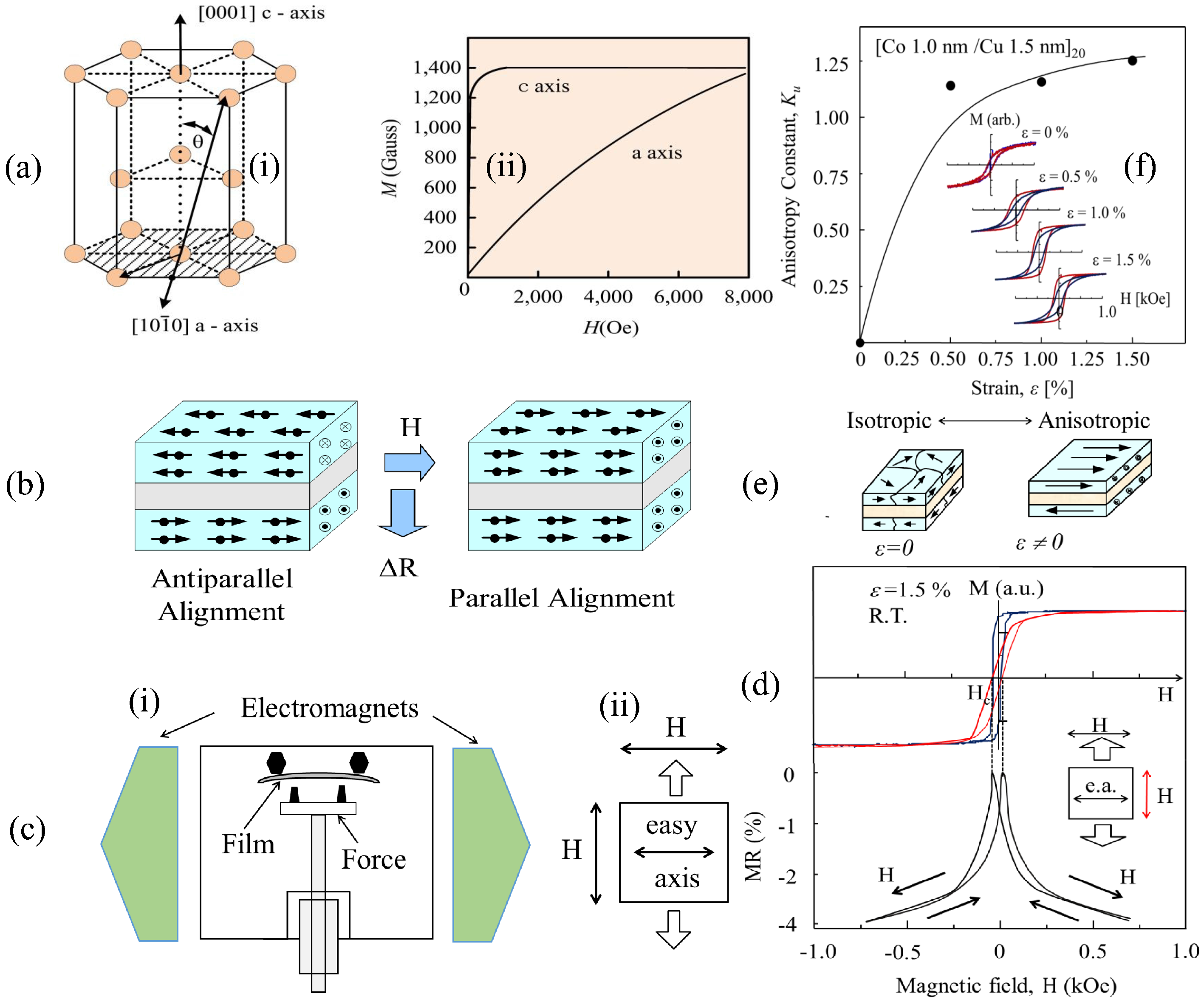
  33. Den Broeder, F.; Hoving, W.; Bloemen, P. Magnetic anisotropy of multilayers. J. Magn. Magn. Mater. 1991, 93, 562–570. [Google Scholar] [CrossRef]
  34. Rizal, C.; Niraula, B.B. Ferromagnetic alloys: Magnetoresistance, microstructure, magnetism, and beyond (Review). J. Nano Electron. Phys. 2015, 7, 04068-1–04068-16. [Google Scholar]
  35. Rizal, C.; Wingert, J.; Fullerton, E.E. Perpendicular magnetic anisotropy and microstructure properties of Ta/Co (tCo)/Au (tAu) multilayers. In Proceedings of the Joint IEEE Magnetics and MMM Conferences, San Diego, CA, USA, 11–15 January 2016.
  36. Chikazumi, S.; Graham, C.D. Physics of Ferromagnetism, 2nd ed.; Oxford University Press: Oxford, UK, 1997; p. 655. [Google Scholar]
  37. Coey, J.M.D. Magnetism and Magnetic Materials, 1st ed.; Cambridge University Press: Cambridge, UK, 2010; p. 614. [Google Scholar]
  38. Cullity, B.D.; Graham, C.D. Introduction to Magnetic Materials, 2nd ed.; Wiley: Piscataway, NJ, USA; Hoboken, NJ, USA, 2009; p. 544. [Google Scholar]
  39. Chikazumi, S. Physics of Magnetism; Krieger: Malabar, FL, USA, 1978; Volume 153, p. 338. [Google Scholar]
  40. Rizal, C.; Gyawali, P.; Kshatry, I.; Pokharel, R.K. Strain-induced magnetoresistance and magnetic anisotropy of Co/Cu multilayers. J. Appl. Phys. 2012, 111. [Google Scholar] [CrossRef]
  41. Rizal, C. Study of magnetic anisotropy and magnetoresistance effects in ferromagnetic Co/Au multilayer films prepared by oblique incidence evaporation method. J. Magn. Magn. Mater. 2007, 310, e646–e648. [Google Scholar] [CrossRef]
  42. Thomson, W. On the electrodynamic qualities of metals: Effects of magnetization on the electric conductivity of Nickel and Iron. Proc. R. Soc. Lond. 1857, 8, 546–550. [Google Scholar] [CrossRef]
  43. McGuire, T.; Potter, R. Anisotropic magnetoresistance in ferromagnetic 3-d alloys. IEEE Trans. Magn. 1975, 11, 1018–1038. [Google Scholar] [CrossRef]
  44. Florczak, J.M.; Dahlberg, E.D.; Fullerton, E.E.; Schuller, I.K. Magnetotransport properties of Fe/Cu multilayer films. J. Appl. Phys. 1991, 70, 5836. [Google Scholar] [CrossRef]
  45. Fullerton, E.E.; Schuller, I.K. The 2007 Nobel Prize in physics: Magnetism and transport at the nanoscale. ACS Nano 2007, 1, 384–389. [Google Scholar] [CrossRef] [PubMed]
  46. Parkin, S.S.P. Giant magnetoresistance in magnetic nanostructures. Annu. Rev. Mater. Sci. 1995, 25, 357–388. [Google Scholar] [CrossRef]
  47. Ruderman, M.A.; Kittel, C. Indirect exchange coupling of nuclear magnetic moments by conduction electrons. Phys. Rev. 1954, 96. [Google Scholar] [CrossRef]
  48. Kasuya, T. A theory of metallic ferro-and antiferromagnetism on Zener’s model. Prog. Theor. Phys. 1956, 16, 45–57. [Google Scholar] [CrossRef]
  49. Yosida, K. Magnetic properties of Cu-Mn alloys. Phys. Rev. 1957, 106. [Google Scholar] [CrossRef]
  50. Bruno, P.; Chappert, C. Ruderman-Kittel theory of oscillatory interlayer exchange coupling. Phys. Rev. B 1992, 46. [Google Scholar] [CrossRef]
  51. Bruno, P.; Chappert, C. Oscillatory coupling between ferromagnetic layers separated by a nonmagnetic metal spacer. Phys. Rev. Lett. 1991, 67, 1602–1605. [Google Scholar] [CrossRef] [PubMed]
  52. Bakonyi, I.; Tóth-Kádár, E.; Cziráki, Á.; Tóth, J.; Kiss, L.; Ulhaq-Bouillet, C.; Pierron-Bohnes, V.; Dinia, A.; Arnold, B.; Wetzig, K. Preparation, structure, magnetic, and magnetotransport properties of electrodeposited Co (Ru)/Ru multilayers. J. Electrochem. Soc. 2002, 149, C469–C473. [Google Scholar] [CrossRef]
  53. Monchesky, T.; Heinrich, B.; Urban, R.; Myrtle, K.; Klaua, M.; Kirschner, J. Magnetoresistance and magnetic properties of Fe/Cu/GaS (100). Phys. Rev. B 1999, 60. [Google Scholar] [CrossRef]
  54. Sugiyama, T.; Nittono, O. Structure and giant magnetoresistance of Co/Ag granular alloy film fabricated by a multilayering method. Thin Solid Films 1998, 334, 206–208. [Google Scholar] [CrossRef]
  55. Suenaga, K.; Oomi, G.; Uwatoko, Y.; Saito, K.; Takanashi, K.; Fujimori, H. Study of strain and giant magnetoresistance of Co/Cu magnetic multilayers. Phys. Soc. Jpn. 2006, 75, 747151–747155. [Google Scholar]
  56. Rizal, C.; Gyawali, P.; Kshattry, I.; Ueda, Y.; Pokharel, R. Effect of strain on MR and magnetic properties of Co(tCo)/Ag nanostructures. In Proceedings of the 2011 IEEE Nanotechnology Materials and Devices Conference (NMDC), Jeju, Korea, 18–21 October 2011.
  57. Hyomi, K.; Murayama, A.; Oka, Y.; Falco, C.M. Misfit strain and magnetic anisotropies in ultrathin Co films hetero epitaxially grown on Au/Cu/Si(1 1 1). J. Cryst. Growth 2002, 235, 567–571. [Google Scholar] [CrossRef]
  58. Rizal, C.; Fullerton, E.E. Magnetic, Microstructure, and Plasma-Enhanced Magneto-Optic Properties of Ta/Au(tAu)/Co (tCo)/Au (tAu) Nanostructures. In Proceedings of the Material Research Society, San Francisco, CA, USA, 4 August 2016.
  59. Rizal, C. Magnetotransport properties of Co(tCo)/Cu(tCu) multilayer films. In Proceedings of the IEEE Joint Intermag-MMM Conference, Washington, DC, USA, 18–22 January 2010; p. 2.
  60. Yamada, A.; Houga, T.; Ueda, Y. Magnetism and magnetoresistance of Co/Cu multilayer films produced by pulse control electrodeposition method. J. Magn. Magn. Mater. 2002, 239, 272–275. [Google Scholar] [CrossRef]
  61. Ueda, Y.; Ikeda, S.; Hama, S.; Yamada, A. Magnetic properties and magnetoresistance of Fe/Cr multilayer films prepared by vapor deposition and electrodeposition. J. Magn. Magn. Mater. 1996, 156, 353–354. [Google Scholar] [CrossRef]
  62. Rizal, C.; Ueda, Y.; Pokharel, R.K. Magnetotransport properties of Co-Au granular alloys. Int. J. Appl. Phys. Math. 2011, 1, 161–166. [Google Scholar] [CrossRef]
  63. Bao, Z.L.; Kavanagh, K.L. Aligned Co nanodiscs by electrodeposition on GaAs. J. Cryst. Growth 2006, 287, 514–517. [Google Scholar]
  64. Rajasekaran, N.; Mohan, S.; Jagannathan, R. Giant magnetoresistance and ferromagnetic properties of DC and pulse electrodeposited CuCo alloys. J. Magn. Magn. Mater. 2012, 324, 2983–2988. [Google Scholar] [CrossRef]
  65. Bakonyi, I. Electrodeposited multilayer films with giant magnetoresistance (GMR): Progress and problems. Prog. Mater. Sci. 2010, 55, 107–245. [Google Scholar] [CrossRef]
  66. Brenner, A. Electrodeposition of Alloys Principle and Practice; Academic Press: New York, NY, USA, 1963. [Google Scholar]
  67. Puippe, J.C.; Leaman, F. Theory and Practice of Pulse Plating; The American Electroplaters and Surface Finishers Society: Orlando, FL, USA, 1986. [Google Scholar]
  68. Yuasa, S.; Nagahama, T.; Fukushima, A.; Suzuki, Y.; Ando, K. Giant room temperature magnetoresistance in single crystal Fe/MgO/Fe magnetic tunnel junctions. Nat. Mater. 2004, 3, 868–871. [Google Scholar] [CrossRef] [PubMed]
  69. Miyazaki, T.; Tezuka, N. Giant magnetic tunneling effect in Fe/Al2O3/Fe junction. J. Magn. Magn. Mater. 1995, 139, L231–L234. [Google Scholar] [CrossRef]
  70. Moodera, J.S.; Kinder, L.R.; Wong, T.M.; Meservey, R. Large magnetoresistance at room temperature in ferromagnetic thin film tunnel junctions. Phys. Rev. Lett. 1995, 74, 3273–3276. [Google Scholar] [CrossRef] [PubMed]
  71. Hayakawa, J.; Ikeda, S.; Lee, Y.M.; Matsukura, F.; Ohno, H. Effect of high annealing temperature on giant tunnel magnetoresistance ratio of CoFeB/MgO/CoFeB magnetic tunnel junctions. Appl. Phys. Lett. 2006. [Google Scholar] [CrossRef]
  72. Takanashi, K. Fundamentals of Magnetoresistance Effects. In Spintronics for Next Generation Innovative Devices; Wiley: New York, NY, USA, 2015; p. 1. [Google Scholar]
  73. Bowen, M.; Bibes, M.; Barthélémy, A.; Contour, J.P.; Anane, A.; Lemaıtre, Y.; Fert, A. Nearly total spin polarization in La2/3Sr1/3MnO3 from tunneling experiments. Appl. Phys. Lett. 2003, 82, 233–235. [Google Scholar] [CrossRef]
  74. Bratkovsky, A. Tunneling of electrons in conventional and half-metallic systems: Towards very large magnetoresistance. Phys. Rev. B 1997, 56. [Google Scholar] [CrossRef]
  75. Majumdar, S.; van Dijken, S. Pulsed laser deposition of La1−xSrxMnO3: Thin film properties and spintronic applications. J. Phys. D Appl. Phys. 2013, 47. [Google Scholar] [CrossRef]
  76. Greullet, F.; Snoeck, E.; Tiusan, C.; Hehn, M.; Lacour, D.; Lenoble, O.; Magen, C.; Calmels, L. Large inverse magnetoresistance in fully epitaxial Fe/Fe3O4/MgO/Co magnetic tunnel junctions. Appl. Phys. Lett. 2008, 92. [Google Scholar] [CrossRef]
  77. Ramirez, A. Colossal magnetoresistance. J. Phys. Condens. Matter 1997, 9. [Google Scholar] [CrossRef]
  78. Uehara, M.; Mori, S.; Chen, C.; Cheong, S.W. Percolative phase separation underlies colossal magnetoresistance in mixed valent manganites. Nature 1999, 399, 560–563. [Google Scholar]
  79. Almeida, T.M.D.; Piedade, M.S.; Sousa, L.A.; Germano, J.; Lopes, P.A.; Cardoso, F.A.; Freitas, P.P. On the modeling of new tunnel junction magnetoresistive biosensors. IEEE Trans. Instrum. Meas. 2010, 59, 92–100. [Google Scholar] [CrossRef]
  80. Coughlin, T. Thanks for the memories: Nonvolatile memory technology enables the age of spin [The art of storage]. IEEE Consum. Electron. Mag. 2014, 3, 85–92. [Google Scholar] [CrossRef]
  81. Andre, T.; Alam, S.M.; Gogl, D. Memory Device With Reduced on Chip Noise. U.S. Patent US20140104963 A1, 17 April 2014. [Google Scholar]
  82. Slonczewski, J.C. Current-driven excitation of magnetic multilayers. J. Magn. Magn. Mater. 1996, 159, L1–L7. [Google Scholar] [CrossRef]
  83. Berger, L. Emission of spin waves by a magnetic multilayer traversed by a current. Phys. Rev. B 1996, 54, 9353–9358. [Google Scholar] [CrossRef]
  84. Huai, Y.; Albert, F.; Nguyen, P.; Pakala, M.; Valet, T. Observation of spintransfer switching in deep submicron sized and low resistance magnetic tunnel junctions. Appl. Phys. Lett. 2004, 84. [Google Scholar] [CrossRef]
  85. Gallagher, W.J.; Parkin, S.S. Development of the magnetic tunnel junction MRAM at IBM: From first junctions to a 16 MBite MRAM demonstrator chip. IBM J. Res. Dev. 2006, 50, 5–23. [Google Scholar] [CrossRef]
  86. Rowlands, G.E.; Krivorotov, I.N. Magnetization dynamics in a dual freelayer spin-torque nano-oscillator. Phys. Rev. B 2012, 86. [Google Scholar] [CrossRef]
  87. Villard, P.; Ebels, U.; Houssameddine, D.; Katine, J.; Mauri, D.; Delaet, B.; Vincent, P.; Cyrille, M.C.; Viala, B.; Michel, J.P.; et al. A GHz spintronic-based RF oscillator. IEEE J. Solid State Circuits 2010, 45, 214–223. [Google Scholar] [CrossRef]
  88. Krishnan, K.M. Biomedical nanomagnetics: A spin through possibilities in imaging, diagnostics, and therapy. IEEE Trans. Magn. 2010, 46, 2523–2558. [Google Scholar] [CrossRef] [PubMed]
  89. Osterfeld, S.J.; Yu, H.; Gaster, R.S.; Caramuta, S.; Xu, L.; Han, S.J.; Hall, D.A.; Wilson, R.J.; Sun, S.; White, R.L.; et al. Multiplex protein assays based on real-time magnetic nanotag sensing. Proc. Natl. Acad. Sci. USA 2008, 105, 20637–20640. [Google Scholar] [CrossRef] [PubMed]
  90. Jing, Y.; He, S.; Kline, T.; Xu, Y.; Wang, J.P. High-magnetic-moment nanoparticles for biomedicine. In Proceedings of the IEEE Annual International Conference: Engineering in Medicine and Biology Society, San Diego, CA, USA, 2–6 September 2009; pp. 4483–4486.
  91. Wasa, K.; Kitabatake, M.; Adachi, H.; Makoto, H. Thin Film Materials Technology; William Andrew, Inc.: New York, NY, USA, 2004. [Google Scholar]
  92. Srolovitz, D. Shadowing effects on the microstructure of obliquely deposited films. J. Appl. Phys. 2002, 91, 1963–1972. [Google Scholar]
  93. Tang, F.; Liu, D.L.; Ye, D.; Zhao, Y.; Lu, T.; Wang, G.; Vijayaraghavan, A. Magnetic properties of Co nanocolumns fabricated by oblique angle deposition. J. Appl. Phys. 2003, 93, 4194–4200. [Google Scholar] [CrossRef]
  94. Takakura, W.; Ikeda, S.; Ueda, Y. Electrical resistance in Fe/Al2O3 multilayered films prepared by an electron beam evaporation method. Mater. Trans. 2001, 42, 881–885. [Google Scholar] [CrossRef]
  95. Ueda, Y.; Takahashi, M. Structure and magnetic properties in single-crystal iron film electrodeposited on a (110) copper crystal. J. Magn. Magn. Mater. 1988, 71, 212–218. [Google Scholar] [CrossRef]
  96. Chikazumi, S.; Oomura, T. On the origin of magnetic anisotropy induced by magnetic annealing. J. Phys. Soc. Jpn. 1955, 10, 842–849. [Google Scholar] [CrossRef]
  97. Yamada, A.; Shirota, M.; Houga, T.; Rizal, C.; Ueda, Y. Electric and magnetic properties of FeNi based particle and multilayer films produced by pulse control electrodeposition method. J. Jpn. Inst. Metals 2002, 66, 869–872. [Google Scholar]
  98. Rizal, C. Giant Magnetoresistance and Magnetic Properties of Ferromagnetic Hybrid Nanostructures. Ph.D. Thesis, The University of British Columbia, Vancouver, BC, Canada, 26 May 2012. [Google Scholar]
  99. Rizal, C.; Ueda, Y.; Karki, B.R. Magnetic properties of Fe/Cu multilayers prepared using pulsed current electrodeposition. J. Nano Electron. Phys. 2012, 4, 01001-1–01001-3. [Google Scholar]
  100. Gomez, E.; Torres, J.G.; Valles, E. Electrodeposition of CoAg films and compositional determination by electrochemical methods. Anal. Chim. Acta 2007, 60, 187–194. [Google Scholar] [CrossRef] [PubMed]
  101. Torres, J.G.; Peter, L.; Revesz, A.; Pogany, L.; Bakonyi, I. Preparation and giant magnetoresistance of electrodeposited CoAg/Ag multilayers. Thin Solid Films 2009, 517, 6081–6090. [Google Scholar] [CrossRef]
  102. Guan, M.; Podlaha, E.J. Electrodeposition of AuCo alloys and multilayers. J. Appl. Electrochem. 2007, 37. [Google Scholar] [CrossRef]
  103. Baskaran, I.; Narayanan, T.S.; Stephen, A. Pulsed electrodeposition of nanocrystalline CuNi alloy films and evaluation of their characteristic properties. Mater. Lett. 2006, 60, 1990–1995. [Google Scholar] [CrossRef]
  104. Kenane, S.; Voiron, J.; Benbrahim, N.; Chainet, E.; Robaut, F. Magnetic properties and giant magnetoresistance in electrodeposited CoAg granular films. J. Magn. Magn. Mater. 2006, 297, 99–106. [Google Scholar] [CrossRef]
  105. Houga, T.; Yamada, A.; Ueda, Y. Resistivity and magnetism of Co/Cu films produced by computer controlled pulse electrodeposition. J. Jpn. Inst. Met. 2000, 64, 739–742. [Google Scholar]
  106. Ueda, Y.; Houga, T.; Zaman, H.; Yamada, A. Magnetoresistance effect of CoCu nanostructure prepared by electrodeposition method. J. Solid State Chem. 1999, 147, 274–280. [Google Scholar] [CrossRef]
  107. Houga, T.; Zaman, H.; Chikazawa, S.; Ueda, Y. Magnetism and magnetoresistance effect in the CoCu and CoAg films produced by pulse electrodeposition. In Proceedings of the IEEE International Magnetics Conference, Tokyo, Japan, 18–21 May 1999.
  108. Zaman, H.; Ikeda, S.; Ueda, Y. Magnetoresistance in CoAg multilayers and granular films produced by electrodeposition method. IEEE Trans. Magn. 1997, 33, 3517–3519. [Google Scholar] [CrossRef]
  109. Santos, E.; Abbate, M.; Fernandes, V.; Mattoso, N. Electronic structure of metastable Fe1−x Cox alloys produced by electrodeposition. Electrochem. Solid State Lett. 2003, 6, C85–C87. [Google Scholar] [CrossRef]
  110. Scheck, C.; Evans, P.; Schad, R.; Zangari, G.; Williams, J.; Isaacs-Smith, T.F. Structure and magnetic properties of electrodeposited Ni films on nGaAs(001). J. Phys. Condens. Matter 2002, 14. [Google Scholar] [CrossRef]
  111. Valizadeh, S.; Svedberg, E.B.; Leisner, P. Electrodeposition of compositionally modulated Au/Co alloy layers. J. Appl. Electrochem. 2002, 32, 97–104. [Google Scholar] [CrossRef]
  112. Rizal, C.; Yamada, A.; Hori, Y.; Ishida, S.; Matsuda, M.; Ueda, Y. Magnetic properties and magnetoresistance effect in Co/Au, Ag nanostructure films produced by pulse electrodeposition. Phys. Status Solidi C Conf. 2004, 1, 1756–1759. [Google Scholar] [CrossRef]
  113. Rizal, C.; Yamada, A.; Ueda, Y. Pulse electrodeposition of Co/Au multilayers and granular alloys. Jpn. J. Appl. Surf. Finish. 2004, 55, 83–84. [Google Scholar] [CrossRef]
  114. Yamada, A.; Rizal, C.; Murata, S.; Ueda, Y. Electric properties of NiCo based multilayer films produced by pulse control electrodeposition method. J. Surf. Finish. Soc. Jpn. 2004, 55, 151–152. [Google Scholar] [CrossRef]
  115. Rizal, C.; Ueda, Y. Magnetoresistance effect and magnetic properties of strain induced Co/Cu multilayer films. In Proceedings of the 3rd International Nanoelectronics Conference (INEC), Hong Kong, China, 3–8 January 2010; pp. 927–928.
  116. Geoghegan, D.S.; Hutten, A.; Muller, K.H.; Schultz, L. Magnetoresistance of melt spun gold cobalt. J. Magn. Magn. Mater. 1998, 177–181, 1478–1479. [Google Scholar] [CrossRef]
  117. Hutten, A.; Bernardi, J.; Friedrichs, S.; Thomas, G.; Balcells, L. Microstructural influence on magnetic properties and giant magnetoresistance of melt spun AuCo. Scr. Metall. Mater. 1995, 33, 1647–1666. [Google Scholar] [CrossRef]
  118. Ikeda, S.; Houga, T.; Takakura, W.; Ueda, Y. Magnetoresistance in (CoxFe1−x)(20)Cu80 granular alloys produced by mechanical alloying. Mater. Sci. Eng. A 1996, 217, 376–380. [Google Scholar] [CrossRef]
  119. Jones, B.A.; Hanna, C. Contribution of quantum-well states to the RKKY coupling in magnetic multilayers. Phys. Rev. Lett. 1993, 71. [Google Scholar] [CrossRef] [PubMed]
  120. Camley, R.E.; Barnaś, J. Theory of giant magnetoresistance effects in magnetic layered structures with antiferromagnetic coupling. Phys. Rev. Lett. 1989, 63. [Google Scholar] [CrossRef] [PubMed]
  121. Barnaś, J.; Bruynseraede, Y. Electronic transport in ultrathin magnetic multilayers. Phys. Rev. B 1996, 53, 5449–5460. [Google Scholar] [CrossRef]
  122. Valet, T.; Fert, A. Classical theory of perpendicular giant magnetoresistance in magnetic multilayers. J. Magn. Magn. Mater. 1993, 121, 378–382. [Google Scholar] [CrossRef]
  123. Levy, P.M.; Shi, Z.P.; Zhang, S.; Camblong, H.E.; Fry, J.L. Interlayer coupling and magnetoresistance of multilayered structures. J. Magn. Magn. Mater. 1993, 121, 357–361. [Google Scholar] [CrossRef]
  124. Camblong, H.E.; Levy, P.M. Novel results for quasiclassical linear transport in metallic multilayers. Phys. Rev. Lett. 1992, 69, 2835–2838. [Google Scholar] [CrossRef] [PubMed]
  125. Asano, Y.; Oguri, A.; Maekawa, S. Parallel and perpendicular transport in multilayered structures. Phys. Rev. B 1993, 48, 6192–6198. [Google Scholar] [CrossRef]
  126. Itoh, H.; Inoue, J.; Maekawa, S. Theory of giant magnetoresistance for parallel and perpendicular currents in magnetic multilayers. Phys. Rev. B 1995, 51, 342–352. [Google Scholar] [CrossRef]
  127. Todorov, T.; Tsymbal, E.Y.; Pettifor, D. Giant magnetoresistance: Comparison of band structure and interfacial-roughness contributions. Phys. Rev. B 1996, 54. [Google Scholar] [CrossRef]
  128. Schep, K.M.; Kelly, P.J.; Bauer, G.E. Giant magnetoresistance without defect scattering. Phys. Rev. Lett. 1995, 74, 586–589. [Google Scholar] [CrossRef] [PubMed]
  129. Oguchi, T. Fermi velocity effect on magnetoresistance in Fe/transition metal multilayers. J. Magn. Magn. Mater. 1993, 126, 519–520. [Google Scholar] [CrossRef]
  130. Binder, S.; Langhammer, J.; Calci, A.; Navratil, P.; Roth, R. Ab initio calculations of medium-mass nuclei with explicit chiral 3N interactions. Phys. Rev. C 2013, 87. [Google Scholar] [CrossRef]
  131. Butler, W.; Zhang, X.G.; Nicholson, D.; MacLaren, J. First-principles calculations of electrical conductivity and giant magnetoresistance of Co/Cu/Co spin valves. Phys. Rev. B 1995, 52, 13399–13410. [Google Scholar] [CrossRef]
  132. Tsymbal, E.Y.; Pettifor, D. Perspectives of giant magnetoresistance. Solid State Phys. 2001, 56, 113–237. [Google Scholar]
  133. Blaas, C.; Weinberger, P.; Szunyogh, L.; Levy, P.; Sommers, C. Ab initio calculations of magnetotransport for magnetic multilayers. Phys. Rev. B 1999, 60. [Google Scholar] [CrossRef]
  134. Hartmann, U. Springer Series in Surface Sciences; Springer: Berlin, Germany, 2000; p. 321. [Google Scholar]
  135. McFadyen, I.; Fullerton, E.; Carey, M. State-of-the-art magnetic hard disk drives. MRS Bull. 2006, 31, 379–383. [Google Scholar] [CrossRef]
  136. Grochowski, E. Emerging trends in data storage on magnetic hard disk drives. Available online: https://courses.cs.washington.edu/courses/cse590s/03au/grochowski-trends.pdf (accessed on 13 April 2016).
  137. Belleson, J.; Grochowski, E. The era of giant magnetoresistive heads. Available online: https://www1.hgst.com/hdd/technolo/gmr/gmr.htm (accessed on 13 April 2016).
  138. Pannetier, M.; Fermon, C.; Legoff, G.; Simola, J.; Kerr, E.; Welling, M.; Wijngaarden, R.J. Ultra-sensitive field sensors-an alternative to SQUIDs. IEEE Trans. Appl. Supercond. 2005, 15, 892–895. [Google Scholar] [CrossRef]
  139. Pannetier-Lecoeur, M.; Polovy, H.; Sergeeva-Chollet, N.; Cannies, G.; Fermon, C.; Parkkonen, L. Magnetocardiography with GMR-Based Sensors; IOP Publishing: Bristol, UK, 2011. [Google Scholar]
  140. Kotitz, R.; Matz, H.; Trahms, L.; Koch, H.; Weitschies, W.; Rheinlander, T.; Semmler, W.; Bunte, T. SQUID based remanence measurements for immunoassays. IEEE Trans. Appl. Supercond. 1997, 7, 3678–3681. [Google Scholar] [CrossRef]
  141. Baselt, D.R.; Lee, G.U.; Natesan, M.; Metzger, S.W.; Sheehan, P.E.; Colton, R.J. A biosensor based on magnetoresistance technology. Biosens. Bioelectron. 1998, 13, 731–739. [Google Scholar] [CrossRef]
  142. Edelstein, R.; Tamanaha, C.; Sheehan, P.; Miller, M.; Baselt, D.; Whitman, L.; Colton, R. The BARC biosensor applied to the detection of biological warfare agents. Biosens. Bioelectron. 2000, 14, 805–813. [Google Scholar] [CrossRef]
  143. Han, S.J.; Yu, H.; Murmann, B.; Pourmand, N.; Wang, S.X. A high-density magnetoresistive biosensor array with drift compensation mechanism. In Proceedings of the 2007 IEEE International Solid-State Circuits Conference (Digest of Technical Papers), San Francisco, CA, USA, 11–15 February 2007.
  144. Ferreira, H.; Feliciano, N.; Graham, D.; Freitas, P. Effect of spin valve sensor magnetostatic fields on nanobead detection for biochip applications. J. Appl. Phys. 2005, 97. [Google Scholar] [CrossRef]
  145. Boer, B.D.; Kahlman, J.; Jansen, T.; Duric, H.; Veen, J. An integrated and sensitive detection platform for magneto-resistive biosensors. Biosens. Bioelectron. 2007, 22, 2366–2370. [Google Scholar] [CrossRef] [PubMed]
  146. Koets, M.; der Wijk, T.V.; Eemeren, J.V.; Amerongen, A.V.; Prins, M. Rapid DNA multi-analyte immunoassay on a magnetoresistance biosensor. Biosens. Bioelectron. 2009, 24, 1893–1898. [Google Scholar] [CrossRef] [PubMed]
  147. Graham, D.L.; Ferreira, H.A.; Freitas, P.P. Magnetoresistive based biosensors and biochips. Trends Biotechnol. 2004, 22, 455–462. [Google Scholar] [CrossRef] [PubMed]
  148. Germano, J.; Martins, V.C.; Cardoso, F.A.; Almeida, T.M.; Sousa, L.; Freitas, P.P.; Piedade, M.S. A portable and autonomous magnetic detection platform for biosensing. Sensors 2009, 9, 4119–4137. [Google Scholar] [CrossRef] [PubMed]
  149. Reiss, G.; Brueckl, H.; Huetten, A.; Schotter, J.; Brzeska, M.; Panhorst, M.; Sudfeld, D.; Becker, A.; Kamp, P.B.; Puehler, A.; et al. Magnetoresistive sensors and magnetic nanoparticles for biotechnology. J. Mat. Res. 2005, 20, 3294–3302. [Google Scholar] [CrossRef]
  150. Schotter, J.; Kamp, P.B.; Becker, A.; PÃhler, A.; Reiss, G.; Bruckl, H. Comparison of a prototype magnetoresistive biosensor to standard fluorescent DNA detection. Biosens. Bioelectron. 2004, 19, 1149–1156. [Google Scholar] [CrossRef] [PubMed]
  151. Srinivasan, B.; Li, Y.; Jing, Y.; Xu, Y.H.; Yao, X.; Xing, C.; Wang, J.P. A detection system based on giant magnetoresistive sensors and high—Moment magnetic nanoparticles demonstrates zeptomole sensitivity: Potential for personalized medicine. Angew. Chem. Int. Ed. 2009, 48, 2764–2767. [Google Scholar] [CrossRef] [PubMed]
  152. Xu, L.; Yu, H.; Akhras, M.S.; Han, S.J.; Osterfeld, S.; White, R.L.; Pourmand, N.; Wang, S.X. Giant magnetoresistive biochip for DNA detection and HPV genotyping. Biosens. Bioelectron. 2008, 24, 99–103. [Google Scholar] [CrossRef] [PubMed]
  153. Wang, H. Magnetic sensors for diagnostic medicine: CMOS based magnetic particle detectors for medical diagnosis applications. IEEE Microw. Mag. 2013, 14, 110–130. [Google Scholar] [CrossRef]
  154. Wang, S.X.; Li, G. Advances in giant magnetoresistance biosensors with magnetic nanoparticle tags: Review and outlook. IEEE Trans. Magn. 2008, 44, 1687–1702. [Google Scholar] [CrossRef]
  155. Reig, C.; Cubells-Beltrán, M.D.; Ramírez Muńoz, D. Magnetic field sensors based on giant magnetoresistance (GMR) technology: Applications in electrical current sensing. Sensors 2009, 9, 7919–7942. [Google Scholar] [CrossRef] [PubMed]
  156. Jogschies, L.; Klaas, D.; Kruppe, R.; Rittinger, J.; Taptimthong, P.; Wienecke, A.; Rissing, L.; Wurz, M.C. Recent developments of magnetoresistive sensors for industrial applications. Sensors 2015, 15, 28665–28689. [Google Scholar] [CrossRef] [PubMed]
  157. Van den Berg, H.; Coehoorn, R.; Gijs, M.; Grünberg, P.; Rasing, T.; Röll, K.; Hartmann, U. Magnetic Multilayers and Giant Magnetoresistance: Fundamentals and Industrial Applications; Springer Science & Business Media; Springer: New York, NY, USA, 2013; Volume 37. [Google Scholar]
  158. Jander, A.; Smith, C.; Schneider, R. Magnetoresistive sensors for nondestructive evaluation. In Proceedings of the Advanced Sensor Technologies for Nondestructive Evaluation and Structural Health Monitoring, San Diego, CA, USA, 6 March 2005.
  159. Tian, G.Y.; Sophian, A.; Taylor, D.; Rudlin, J. Multiple sensors on pulsed eddy-current detection for 3-D subsurface crack assessment. IEEE Sens. J. 2005, 5, 90–96. [Google Scholar] [CrossRef]
  160. Lang, Z.; Agurto, A.; Tian, G.; Sophian, A. A system identification based approach for pulsed eddy current non-destructive evaluation. Meas. Sci. Technol. 2007, 18, 2083–2091. [Google Scholar] [CrossRef]
  161. Simm, A.; Theodoulidis, T.; Poulakis, N.; Tian, G.Y. Investigation of the magnetic field response from eddy current inspection of defects. Int. J. Adv. Manuf. Technol. 2011, 54, 223–230. [Google Scholar] [CrossRef]
  162. Cui, Z.; Wang, X.; Li, Y.; Tian, G.Y. High sensitive magnetically actuated micromirrors for magnetic field measurement. Sens. Actuators A Phys. 2007, 138, 145–150. [Google Scholar] [CrossRef]
  163. McGary, P.D.; Tan, L.; Zou, J.; Stadler, B.J.; Downey, P.R.; Flatau, A.B. Magnetic nanowires for acoustic sensors. J. Appl. Phys. 2006, 99. [Google Scholar] [CrossRef]
  164. Xiong, Z.; Wu, D.; Vardeny, Z.V.; Shi, J. Giant magnetoresistance in organic spin valves. Nature 2004, 427, 821–824. [Google Scholar] [CrossRef] [PubMed]
  165. Choi, B.; Ho, J.; Arnup, G.; Freeman, M. Nonequilibrium domain pattern formation in mesoscopic magnetic thin film elements assisted by thermally excited spin fluctuations. Phys. Rev. Lett. 2005, 95. [Google Scholar] [CrossRef] [PubMed]
  166. Choi, B.; Rudge, J.; Girgis, E.; Kolthammer, J.; Hong, Y.; Lyle, A. Spin current pulse induced switching of vortex chirality in permalloy/Cu/Co nanopillars. Appl. Phys. Lett. 2007, 91. [Google Scholar] [CrossRef]
  167. Katine, J.; Fullerton, E.E. Device implications of spin transfer torques. J. Magn. Magn. Mater. 2008, 320, 1217–1226. [Google Scholar] [CrossRef]
  168. Courtland, R. Spin memory shows its might [News]. IEEE Spectr. 2014, 51, 15–16. [Google Scholar] [CrossRef]
  169. Deac, A.M.; Fukushima, A.; Kubota, H.; Maehara, H.; Suzuki, Y.; Yuasa, S.; Nagamine, Y.; Tsunekawa, K.; Djayaprawira, D.D.; Watanabe, N. Bias driven high power microwave emission from MgO-based tunnel magnetoresistance devices. Nat. Phys. 2008, 4, 803–809. [Google Scholar] [CrossRef]
  170. Schubert, M.; Tiwald, T.E.; Woollam, J.A. Explicit solutions for the optical properties of arbitrary magnetooptic materials in generalized ellipsometry. Appl. Opt. 1999, 38, 177–187. [Google Scholar] [CrossRef] [PubMed]
  171. Stockman, M.I. Nanoplasmonics: The physics behind the applications. Phys. Today 2011, 64, 39–44. [Google Scholar] [CrossRef]
  172. Kretschmann, E. The angular dependence and the polarisation of light emitted by surface plasmons on metals due to roughness. Opt. Commun. 1972, 5, 331–336. [Google Scholar] [CrossRef]
  173. Kretschmann, E. Die bestimmung der oberfa¨ca¨cchenrauhigkeit dunner schichten durch messung der winkelabha¨cngigkeit der streustrahlung von oberfla¨cchenplasmaschwingungen. Opt. Commun. 1974, 10, 353–356. [Google Scholar] [CrossRef]
  174. Alleyne, C.J.; Kirk, A.G.; McPhedran, R.C.; Nicorovici, N.A.P.; Maystre, D. Enhanced SPR sensitivity using periodic metallic structures. Opt. Express 2007, 15, 8163–8169. [Google Scholar] [CrossRef] [PubMed]
  175. Otto, A. Eine neue Methode der Anregung nichtstrahlender Oberfla¨chenplasmaschwingungen. Phys. Status Solidi (b) 1968. [Google Scholar] [CrossRef]
  176. Inoue, M.; Baryshev, A.; Goto, T.; Baek, S.; Mito, S.; Takagi, H.; Lim, P. Magnetophotonic crystals: Experimental realization and applications. In Magnetophotonics; Springer: New York, NY, USA, 2013; pp. 163–190. [Google Scholar]
  177. Rizal, C.; Moa, B.; Brolo, A.G. Recent progress in ferromagnetic multilayer-basesd magnetoplasmonic devices for potential biomedical applications. In Proceedings of the Canadian Medical and Biomedical Engineering Society Series, Vancouver, BC, Canada, 19–23 May 2014; pp. 1–4.
  178. Rizal, C.; Brolo, A.G. Magnetoplasmonics Properties of Co/Au Nanostructures. In Proceedings of the 58th Annual Conference on Magnetism and Magnetic Materials, Denver, CO, USA, 4–8 November 2013.
  179. Rizal, C.; Niraula, B.; Lee, H.W. Bio-magnetoplasmonics, Emerging Biomedical Technologies, and Beyond (Mini Review). J. Nanomed. Res. 2016, 3. [Google Scholar] [CrossRef]
Figure 1. (a-i) Crystallographic orientation of hcp-Co and (a-ii) corresponding magnetization curves. The magnetization prefers to align with a specific crystallographic direction (e.g., the hexagonal axis in Co). The anisotropy constant for pure Co, K u 1 = 5 × 10 6 erg/cc (20 μ eV/atom) [39]. (b) structure showing magnetic alignment from antiparallel to parallel due to H field; (c) Schematic of inducing strain, ϵ in the sample: In (c-i), position of the multilayer films, the direction of the applied mechanical force, and the position of the electromagnets; and (c-ii), directions of the applied mechanical and magnetic forces, and the direction of correspondingly the induced magnetic easy axis, Adapted from [40], Copyright AIP Publishing LLC, 2012; (d) The peak of the GMR corresponding to H c ; (e) FM Multilayers for ϵ = 0 and ϵ ≠ 0 case; (f) A relationship between the magnetic anisotropy constant, K u , and the induced ϵ . The inset shows M-H curves when the ϵ is changed in the range of 1.5%. Adapted from [40], Copyright AIP Publishing LLC, 2012.
Magnetochemistry 02 00022 g001
Figure 2. Schematic showing various functional effects in ferromagnetic (FM), multilayered films (a) Giant magnetoresistance (GMR), effect in Fe/Cr multilayers. Adapted from [1]. (b-i) GMR effect in Fe/Cr multilayers; (b-ii) GMR effect, function as a Cr layer thickness, t C r , measured at room temperature and at 4 K. The GMR effect is periodic in nature and it varies with t C r ; (b-iii) shows the MR measurement arrangement; (c-i, ii) observed magnetic anisotropy. Reproduced with permission from [3], Copyright AIP Publishing LLC, 1993. And (d) new devices using spin functionalities.
Magnetochemistry 02 00022 g002
Figure 3. (a) A Schematic of a Co/Cu multilayer; (b), Magnetoresistance (MR), for the Co/Cu multilayers at room temperature and 4 K (the subscript 30 in the inset indicates the number of bilayers). The MR is oscillatory in nature and it varies with the Cu layer thickness. The peak of the MR curves corresponds to the antiferromagnetic alignment of magnetic moments in the adjacent Co layers as denoted by AFM in the diagram. Reproduced with permission from [46], Copyright Elsevier, 1994.
Magnetochemistry 02 00022 g003
Figure 4. Commonly used fabrication processes: physical vapor deposition and chemical deposition.
Magnetochemistry 02 00022 g004
Figure 5. (a) The normalized electrical resistance versus normalized temperature. Note the electronic configuration, and 3-d and 4-d states of Ni and Pd, respectively, and the order-disorder transition for Ni at T c . Both Ni and Pd follow the same path above T c . Adapted from [42]; (b) Schematic representation of the density of electronic states, N(E), of the 3-d transition FM metals. Note the N(E) is room temperature density of states of s and d states at the Fermi energy, F E , level. At F E , the majority spin states (i.e., spin-ups, ↑) are completely filled while the minority spin states (i.e., spin-downs, ↓ ) are partially filled, and the unequal filling of bands is the main source of net magnetic moment in 3-d transition FM metals [98]; (c) Schematic illustrating two-current model of Mott as applied to 3-d FM metals. The resistivity, ρ arising from the scattering of the 4-s electrons and 3-d electrons are denoted by ρ s s and ρ s d , respectively. The plus and minus signs indicate spin-up and spin-down, respectively [98].
Magnetochemistry 02 00022 g005
Figure 6. (a) Cross-sectional view of a FM/NM multilayer and the scattering of the 4-s conduction electrons (small black arrows crossing the yellow circles) by the local 3-d magnetic moments (big red arrows) (a-i) H = 0; (a-ii) H ≠ 0. The black diagonal arrows represent scattering paths of the 4-s conduction electrons. (b) Mott’s two-current model applied to multilayers: (b-i) H = 0; and (b-ii) H ≠ 0. Black arrows in (b-i, ii) represent current channels [98].
Magnetochemistry 02 00022 g006
Figure 7. (a) Randomly-oriented multi-domains ferromagnetic (FM) multilayers, consisting of isotropic domain of Co; and (b) uniaxially oriented single domain FM multilayers [98].
Magnetochemistry 02 00022 g007
Figure 8. (a) Schematics of biosensing scheme. It consists of giant magnetoresistance (GMR) sensor, which is developed underneath the substrate, bio-conjugated nano-magnetic particles embedded in the cell, antibody, and receptor. The dotted line shows the direction of stray magnetic fields induced by magnetically labeled bio-material (b) Microgram of the post-processed die and scanning electron microscopy images of the spin-valve biosensor array. Adapted from [154].
Magnetochemistry 02 00022 g008
Figure 9. An Everspin spin-transfer-torque based magnetic random access memory chip for caching application. Reproduced with permission from [80], Copyright IEEE, 2014.
Magnetochemistry 02 00022 g009
Figure 10. (a) Measurement configuration of magnetic tunnel junction, MTJ, and spin-transfer torque, STT, nanopillars-based Nano-oscillator, and magnetic, H field and current, I sign conventions; (b) differential magnetoresistance plotted against the H field; Inset shows the enlarged view at the low H field range. Reproduced with permission from [169], Copyright Nature Publishing Group, 2009; (c) Flow chart showing various features of a STT Nano-oscillator.
Magnetochemistry 02 00022 g010
Figure 11. (a-i) Surface plasmon resonance (SPR) and (a-ii) magneto-optic SPR (MO-SPR) effects. Both the SPR and MO-SPR peaks shift towards higher incident angle, θ , with refractive index, n d , of a sample. The sensing response of the MO-SPR configuration is much larger as compared to the sensing response of the SPR configuration for the same shift of refractive index, δ n . Adapted from [11]; (b) The MO-SPR versus θ for four types of samples: The n of the sample is increased from n 1 = 1.7 to n 4 = 2.0, in the increment of 0.1. The figure in the inset shows the MO-SPR sensitivity [177,178].
Magnetochemistry 02 00022 g011
Table 1. Electrochemical parameters. Adapted from [62,108].
Co-AgCo-CuCo-Au
Constituentsg/LConstituentsg/LConstituentsg/L
CoSO 4 · 7 H 2 O5–16CoSO 4 · 7 H 2 O28–39CoSO 4 · 7 H 2 O1–10
AgSO 4 · 7 H 2 O0.1–5.5CuSO 4 · 7 H 2 O15–25AuK(CN) 2 15–25
Na 3 C 6 H 6 O 7 · 7 H 2 O76Na 3 C 6 H 6 O 7 · 7 H 2 O76Na 3 C 6 H 6 O 7 · 7 H 2 O76
NaSO 4 · 10 H 2 O4NaCl2NaCl2
Table 2. Physical parameters and optical properties of ferromagnetic and plasmonic metals, and dielectrics at 298 K, with and without an externally applied magnetic, H, field: ϵ x x is the permittivity of the sample at zero applied H field, ϵ y y is the permittivity induced by the externally applied H field due to an enhanced optical radiation and H field interaction, t = individual layer thickness, L.N. 1 denotes the substrate, and L.N. 6 is the sample under investigation. A 2 nm thick Au layer is used as a cap layer to prevent the surface of the multilayer from oxidation. A 2 nm Ti buffer layer is used to improve adhesion between Au layer and substrate [16,177,179].
Layer Number (L.N.)Materialst (nm) ϵ x x ϵ y y
6Samples6 01 . 70 02 . 00
5Au2 11 . 0 + j 1 . 98
4Co10 11 . 43 + j 18 . 15 0 . 65 + j 0 . 0005
3Au35 11 . 0 + j 1 . 98
2Ti2 04 . 61 + j 2 . 44
1Substrate200002.29

