Abstract
Chemical vapor deposition (CVD) on metal foils is regarded as the most effective method to produce large-area graphene with properties in line with the requirements of an extensive range of electronic and optical applications. For the CVD of graphene, ethanol is a versatile carbon source alternative to the widely used methane. In this review we report on the current progress in this field showing how the CVD parameters can be modulated to gain full microstructural control on graphene grown on Cu foils. Using ethanol vapor, graphene can be grown as a continuous film with mono- or multi-layer thickness, and also in the form of isolated crystals on pre-oxidized Cu substrates. Overall, ethanol-CVD allows a controllable degree of crystallinity and tunable electrical/optical characteristics in the grown samples. In turn, this control translates into a superior versatility for device design and related applications.
1. Introduction
In hindsight, the early observations of atomically thin graphite crystals grown onto metal surfaces exposed to hydrocarbons at high temperature probably did not gain due attention from the scientific world [1]. Carbon-based materials and nanomaterials have since gained considerable interest both for research and industrial applications, and they are now at the core of technological innovation in many fields. Graphene, the basal plane of graphite, was first isolated as two-dimensional material in 2004 [2]. In the following years, graphene has captured the attention of researchers thanks to its electronic and physical properties, such as an extraordinarily high charge carrier mobility, mechanical strength, and chemical stability [2,3,4,5,6]. Graphene was originally obtained in the form of individual and small samples via the “scotch-tape” exfoliation of graphite [5]; nowadays, several advanced techniques have been devised to produce it in large quantities and with reproducible characteristics. In addition to mechanical and chemical exfoliation [2,5,7,8], and to epitaxial growth on SiC [8,9,10,11], chemical vapor deposition (CVD) emerged as the most reliable and cost-effective approach to make graphene in a form applicable to electronics [10,12,13,14,15]. Thermal CVD offers the possibility to tune the growth process by exploring extensive combinations of parameters, such as substrate composition, structure and surface; precursors, gas type, pressure and flow; temperatures; cooling and heating rates; etc. Suitable combinations of parameters can be designed to target the production of graphene with specific properties (e.g., number of layers, domain size, etc.), over large areas, and in manners compatible with the direct fabrication of vertical and lateral heterostructures [16,17,18]. In specific cases, direct CVD growth could lead to high quality heterostructures, obtained through high-temperature dry processes [19,20]. CVD growth of encapsulated graphene in a hexagonal boron nitride/graphene/hexagonal boron nitride heterostructure is also an important achievement, which demonstrated the scalability of high-mobility graphene-based field-effect transistors (FET) [21]. A larger parameter space can be explored if one includes plasmas [19], which is beyond the scope of the present review. From the point of view of electronic applications, in principle single-crystal graphene with large area (a usually broad definition, which in this paper we interpret as ‘wafer-size’, at least 2-inch) would be required to fabricate commercial devices. Large-area graphene samples are then essential to investigate the physical and chemical properties of the material in view of assessing device performances. Other than a large-area production, the control on the number of layers (and their relative stacking orientation) is another crucial requirement, given that this property can completely alter the physical properties of graphene (to the point that it can even become superconductive in some specific conditions) [22].
In recent years, researchers have learned how to gain control of domain size, layer number, grain boundary density, and defects of wafer-scale CVD graphene and have proved that methane is an effective gas precursor for the growth. Methane is a highly stable, saturated molecule, so that the dehydrogenation in the gas phase is highly endothermic [23]. Growth from methane has been tested under a wide range of CVD pressures: atmospheric [24,25,26,27,28,29,30,31,32,33], intermediate to low pressure (0.1–10 Torr) [25,32,34,35,36], and close to vacuum conditions (10−4–10−6 Torr) [25]. Methane’s thermal decomposition requires high temperatures (>1200 °C) [37] and for this reason, the deposition of high-quality graphene from methane generally requires a temperature >950 °C, sufficient for methane to decompose catalytically on metal foil substrates [38]. Along with the high decomposition temperature, methane is extremely flammable and prone to form explosive mixtures with air [39]; while, the use of pressurized cylinders raises safety concerns and usually translates into higher laboratory’s fitting and operation costs. Researchers have recently tried to overcome these disadvantages by exploring aliphatic alcohols (e.g., methanol, ethanol, propanol) as alternative carbon sources [40].
Among these alternative precursors ethanol vapor is a sensible choice [39,40,41,42]. Ethanol decomposes at a much lower temperature than methane [43], allowing growth of carbon-based materials at lower temperatures. Since ethanol is liquid at standard ambient temperature and pressure (SATP) it can be delivered with an inert carrier at low pressure and the CVD system does not require pressurized flammable gas cylinders. The growth system is consequently safer, more compact and requires overall lower costs.
Raman spectroscopy is a fast and non-destructive technique widely used for the characterization of structural properties of carbon-based materials and graphene in particular. It is used to distinguish graphene from graphite and to evaluate the crystalline quality and thickness of graphene films [44,45,46]. The main features of the Raman spectrum of graphene are the G-peak at ~1580 cm−1 due to the in-plane bond- stretching of all pairs of sp2-carbon atoms in both rings and chains, the D-peak at ~1350 cm−1 due to a breathing mode of six-atom rings, and the peak at ~2700 cm−1, often termed as the 2D band since its frequency is approximately twice the D band frequency, that originates from a double resonance Raman process [44,45,46]. Differently from 2D-peak, the D-peak is activated by disorder or defects, such as disordered carbon, edges, or wrinkles. Commonly, the D to G intensity ratio (ID/IG) is used as Raman indicator of crystalline quality of carbon-based materials [47], where small values are indicative of a low defect density. The 2D to G intensity ratio (I2D/IG) is regarded as a qualitative parameter to evidence the presence of very few sheets of graphene: single layer (1L) or bilayer (2L) are characterized by I2D/IG > 1, while in multilayer graphene I2D/IG < 1 [48]. The frequency, the shape and the full width at half maximum (FWHM) of the 2D-peak provide further information on the number and on the stacking order of graphene layers [45]. A single Lorentzian component (FWHM~24 cm−1) effectively reproduces the 2D peak of single-layer graphene, whereas Raman spectrum of multilayer graphene (number of layers > 5) is hardly distinguishable from that of bulk graphite. In turbostratic multilayer graphene, where there is no stacking order between adjacent layers, the 2D-peak is again described by one Lorentzian component but with a larger linewidth (FWHM~45–60 cm−1) and with a frequency upshifted with respect to the 1L graphene [45,46].
Here we provide a concise review of the most important aspects of the graphene growth by ethanol-based CVD on Cu. We offer a summary of the effect of the CVD parameters on the structural properties of graphene, by investigating in detail Raman spectroscopy data. We complement our analysis with data from other analytic techniques, such as optical microscopy, Raman spectroscopy, atomic force microscopy and scanning electron microscopy (AFM, SEM). This review paper is organized in two main sections. The first section concerns the growth of continuous graphene films with quality comparable to those made from methane-CVD, focusing on the role of process temperature, gas flow, and time. In this context, one of the key features of the ethanol-CVD, the possibility of using ultra-fast growth process, will be presented and described. In the second section, the focus will shift to the growth of single-crystal graphene grains, with lateral size in the mm-range and beyond. Here, a comparison will be made between results obtained with methane and ethanol, to provide a perspective on a topic of interest for several nanotechnology applications.
2. Ethanol-CVD Growth of Continuous Graphene Films
2.1. Tuning of Growth Parameters
The first attempts to grow graphene by ethanol-CVD explored temperature ranges lower than those usually reported for methane-CVD (<1000 °C) [39,40,49], in order to lower the overall process costs. Miyata et al. synthesized high-quality monolayer graphene from ethanol on Ni foils at 900 °C and atmospheric pressure [49]. They introduced a “flash cooling” to reduce the duration of the standard cooling process and avoid the decomposition of the synthesized graphene [49].
Following these preliminary results, other researchers explored wider temperature ranges (650–850 °C) (Figure 1a) [40]. Guermoune et al. grew graphene from several liquid alcohols, such as methanol, ethanol and 1-propanol. Their goal was to improve the alcohol-based growth methods and obtain large-area, continuous graphene films with quality comparable to that obtained from methane-CVD [40]. By monitoring the D band in the Raman spectrum of the grown samples [44,45,47], the group found that the improvement in quality (in terms of crystallinity) strongly depended on the temperature: increasing the temperature from 650 to 850 °C, the graphene crystal domain size kept increasing in size, up to 168 nm (Figure 1a) [40].
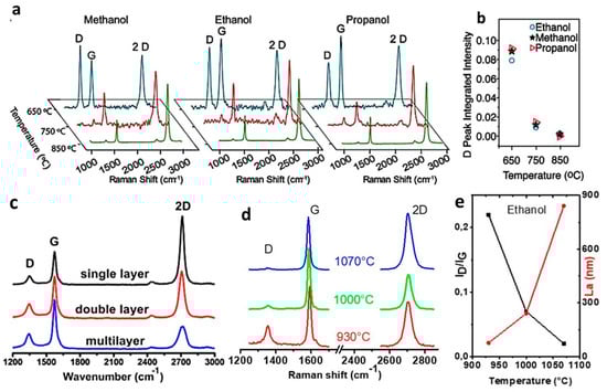
Figure 1.
Raman spectra of graphene films grown by CVD of alcohols at different temperatures. (a) Mono-layer graphene grown at 650, 750 and 850 °C, using methanol, ethanol and propanol (I2D/IG between 2 and 3). Adapted from [40] with permission of Elsevier, Copyright 2011. (b) Integrated intensity of D band corresponding to the Raman spectra of (a). Adapted from [40] with permission of Elsevier, Copyright 2011. (c) Mono-, bi-, and multi-layer graphene grown at 900 °C, using ethanol (t = 30 min): I2D/IG = 2.10 and ID/IG = 0.23. Adapted from [39] with permission of Elsevier, Copyright 2011. (d) Multi-layer graphene films grown at 930, 1000, and 1070 °C, using ethanol (ΦH2 = 100 sccm, t = 30 min). Raman spectrum at 1070 °C: I2D/IG = 1.06 and ID/IG = 0.02. ID/IG and I2D/IG indicate peak intensity ratios. Original data from our group (unpublished). (e) Corresponding ID/IG and crystallite size, La, as a function of temperature. La was calculated according to the general equation La (nm) = 2.4 × 10⁻¹⁰λ4(ID/IG)−1 [50]. Original data from our group (unpublished).
Temperatures below 800 °C were also probed to tune the electronic properties of graphene and use it as functional material in optoelectronics [51]. Dong et al. investigated the CVD of ethanol at atmospheric pressure and 900 °C (for 30 min) [39]. The authors grew a continuous monolayer graphene film with overall low defect density. Some small areas of the film showed Raman spectra representative of bi- and multi-layer graphene, due to the occurrence of secondary nucleation during the growth (Figure 1c) [39]. Higher ethanol-CVD temperatures (930–1070 °C) were investigated and optimized in several studies [52,53,54]. Our group previously studied the effect of process duration (t) and H2 flow rate (ΦH2—used as co-carrier gas with Ar) [52]. At 1070 °C, a process time equal to that set by Dong et al. [39] (30 min) was reported to be enough to obtain multi-layer graphene with the highest crystalline quality (Figure 1d) [52]. Multi-layer graphene could be obtained thanks to a high H2 flow rate (100 sccm): this indicates that hydrogen has a crucial role in the process, which lies in balancing and counteracting the etching effect of water molecules coming from the decomposition of ethanol [52]. Meanwhile, a proper amount of hydrogen (10 sccm) and high temperature (1070 °C) were needed to obtain mono- and bi-layer graphene with high crystalline quality and large crystallite size (280 nm) in only 10 min (Figure 1e) [52].
Despite the initial effort to lower the growth temperature using alcohols rather than methane, the aforementioned studies proved that high temperatures and a substantial flow of hydrogen are key requirements for the growth of graphene with high crystallinity by ethanol-CVD. This seems to be in part related to the lower mobility of carbon atoms on the metal surface when using ethanol instead of methane, which would explain the need for a higher growth temperature [40,52]. Taken together, those results pointed out that ethanol has the potential to replace methane as gas precursor in the CVD growth of continuous graphene films, as long as process temperature above 1000 °C are set (Table 1).

Table 1.
Summary of selected methane and ethanol CVD conditions reported in literature to grow high quality continuous graphene films on Cu foils.
2.2. Ultra-Fast Growth
In order to make the CVD growth suitable for an industrial production, it is important to reduce the process duration as much as possible while maintaining a high material quality [55]. This both increases the production throughput and reduces the thermal loading on the growth substrates. Usually, the growth by methane-CVD requires rather long processes (20–30 min under atmospheric pressure, 30 min under low pressure) [25,34]. Despite this, the possibility to decrease growth time was carefully evaluated in the past [33,56]: as an example of a short process with methane, Li et al. reported the growth of monolayer graphene in 2 min, by using a CH4 flow of 7 sccm (at 6 Pa) at 1035 °C with a partial coverage of Cu substrate [56]. A complete Cu surface coverage was obtained in 3 min by increasing the CH4 flow to 35 sccm [56]. Since then, the mechanism and growth rate of graphene on copper foils have been widely investigated in an extended range of conditions and for various precursors [39,40,57,58,59,60]. As for the CVD of ethanol, Zhao et al. reported a self-limiting growth from ethanol occurring after 5 min at 1000 °C; however this was achieved with a Cu foil enclosure specifically designed to reduce the gas partial pressure at the catalyst surface (and consequently the nucleation rate) [61]. The graphene grown on the internal surface of the Cu foil is uniform (Figure 2a), monolayer and with high quality, as confirmed by Raman spectroscopy (Figure 2b, I2D/IG = 2.0, ID/IG∼0.05) [61].
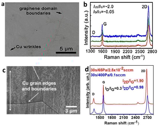
Figure 2.
SEM images and Raman spectra of continuous graphene films grown by ethanol-CVD. (a) SEM image of graphene grown on the internal surface of the Cu enclosure at 1000 °C for 10 min (10 sccm of ethanol and 300 Pa of total pressure) and (b) corresponding Raman spectra taken in three different positions of the same sample transferred on a SiO2/Si substrate. All Raman spectra are indicative of high-quality monolayer graphene and reveal the overall uniformity of the film. Adapted from [61] with permission of American Chemical Society, Copyright 2013. (c) SEM image of graphene grown on copper at 1070 °C for 20 s (0.1 sccm of ethanol, 10 sccm of hydrogen, and 400 Pa of total pressure). Adapted from [38] with permission from Elsevier, Copyright 2014. (d) Raman spectra of graphene, transferred on a SiO2/Si substrate, grown in different conditions (red curve: 30 s for growth time, 65 Pa for total pressure, 2.5 × 10⁻² sccm for ethanol flow rate; blue curve: 30 s for growth time, 400 Pa for total pressure, 0.1 sccm for ethanol flow rate). Original data from our group (unpublished).
Our group explored the initial growth stages of graphene on Cu from ethanol, demonstrating that graphene films can fully cover the copper catalyst substrate in 20 s and less [38]. In this study, the ethanol partial pressure was ~2 Pa and the flow 0.1 sccm, one order of magnitude less than those typical for methane [62], demonstrating that the growth from ethanol is generally quicker than that from methane. However, these continuous films are not entirely monolayer (Figure 2c) but appear polycrystalline and with a high number of wrinkles where, regardless of the short growth time, some secondary nucleation took place [38]. The films also show a residual defect-related D peak (Figure 2d, blue curve), implying that the fast Cu coverage occurs at the expense of the crystalline quality of the film. The graphene thickness could be reduced by throttling down the precursor gas feed. When the ethanol flow rate was decreased from the initial 0.1 to 2.5 × 10⁻² sccm and the total pressure from 400 to 65 Pa (Figure 2d, red curve), a continuous monolayer film could be grown which showed a minor residual D peak (this peak can be further reduced only using longer growth processes).
3. Single-Crystal Graphene Grains: A Comparison between Methane and Ethanol Precursors
CVD graphene is typically poly-crystalline, and the presence of grain boundaries—along with other structural defects—strongly degrades its physical properties, such as charge mobility, thermal conductivity and even mechanical strength [63,64,65]. Many researchers explored the possibility of growing isolated, single-crystal graphene grains (Table 2) [49,56,66,67,68,69,70,71,72,73]. To this end, the first requirement is a significant decrease in nucleation density, in order to delay the coalescence of the grains into a film and allow them to grow bigger. Isolated graphene grains can be designed for specific uses in microelectronics; in this context, the ability to grow oriented grains in a specific pattern would be crucial for their application. The nucleation density of graphene on Cu obtained by methane-CVD was initially in the order of ~106 nuclei/cm2 [66]. Many efforts were made to decrease such a high nucleation density, by carefully modulating the CVD parameters [28,56,69,74,75,76,77]. With the same objective, the Cu substrates were pre-treated by thermal annealing [66,78,79], electrochemical polishing [80], and pre-oxidation [34,78,81,82,83].
Table 2.
Summary of selected methane and ethanol CVD conditions reported in literature to grow high quality single-crystal graphene grains on Cu foils.
Initial efforts (on un-treated Cu substrates) enabled the growth of mm-size graphene grains [33,66,69]. Li et al. grew graphene single crystals with lateral size up to 0.5 mm inside Cu-foil enclosures (Figure 3a) [34]. A small methane flow (less than 1 sccm) and partial pressure (50 mTorr) allowed the growth of large graphene grains with ‘dendritic’ edges. The Raman spectra recorded at two different spots (Figure 3g), one within the film and the other close to the dendrite edge are reported in Figure 3g. The electron mobility in these isolated grains that was higher than 4000 cm2 V−1 s−1 [34]. The search for larger grain sizes pushed researchers to further optimize the methane-CVD process: Tour’s group, for example, grew mm-sized single-crystals (~4.5 mm2) [74]. The growth mechanism was optimized to increase hexagonal-shaped domains from ~15 μm to ~2.3 mm (Figure 3b). Figure 3h shows the Raman spectra recorded at six different spots in Figure 3b: the D peaks are in the noise level indicating samples with very high quality. The authors also fabricated Hall-bar FETs (on Si/SiO2) with the grown graphene, which showed a hole mobility of ~11,000 cm2 V−1 s−1 at room temperature [74]. However, until 2012, a wide variation in domain size, shape, and film quality was recorded from lab to lab, suggesting that crucial growth parameters remained uncontrolled. For this reason, Ruoff’s group demonstrated the possibility to suppress graphene nucleation and promote the growth of ultra large single-crystal graphene domains by pre-oxidizing the Cu foils [81]. The group systematically compared nucleation density, growth rate, and size of graphene grains grown on oxygen-treated Cu foils and produced for the first time cm-sized graphene single crystals (Figure 3c) (decreasing the nucleation density below ~1 nuclei/cm2, i.e., 6 orders of magnitudes less than the initial values) [81]. Since 2013, many groups realized that involving oxygen in the CVD reaction can efficiently reduce the nucleation density, and several procedures were developed to exploit this effect [78,81].
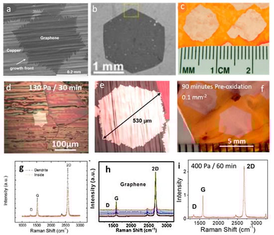
Figure 3.
Growth progression of large single-crystal graphene grains on Cu by CVD of methane (a–c) and ethanol (d–f). (a) SEM image of monolayer single-crystal graphene grain grown at 1035 °C for 90 min (0.5 sccm CH4 flow rate and 8 mTorr CH4 partial pressure) with dimensions of up to 0.5mm and (g) its corresponding Raman spectrum within the bulk of the film and along the dendrite. Adapted from [34] with permission of the American Chemical Society, Copyright 2011. (b) SEM image of one large size mono-layer graphene domain (~2.3 mm) grown at 1077 °C for 125 min (0.15 sccm CH4 flow rate, 70 sccm H2), transferred onto SiO2/Si, and (h) its corresponding Raman spectrum of six different spots. All Raman spectra are indicative of high-quality monolayer graphene and reveal the overall uniformity of the film. Adapted from [74] with permission of the American Chemical Society, Copyright 2012. (c) Photographic image of centimeter-sized single-crystal graphene grown for 12 h on Cu foil after oxidation for 5 min (1.0 × 10⁻³ Torr CH4 partial pressure). Adapted from [81] with permission of The American Association for the Advancement of Science, Copyright 2013. (d) Optical image of mono-layer single-crystal graphene grain with dimensions of up to 90 μm grown at 1070 °C for 30 min (1.5 × 10⁻³ sccm of ethanol and 130 Pa of total pressure). (e) Optical image of the over 500 μm mono-layer graphene grain on Cu grown at 1070 °C for 60 min (1.5 × 10⁻³ sccm of ethanol and 400 Pa of total pressure) and (i) its Raman spectrum after the transfer on Si/SiO2 (I2D/IG = 2.5 and ID/IG = 0.1). Adapted from [84] with permission of the American Chemical Society, Copyright 2018. (f) Hexagonal single-crystal graphene grown at 1065 °C for 22 h (0.03 sccm of ethanol and 300 Pa of total pressure) with dimensions of 5 mm obtained with Cu pre-oxidation for 90 min. Adapted from [67] with permission of Elsevier, Copyright 2015.
The growth of similar individual grains with large size by ethanol-CVD initially lagged behind. In 2015, Chen et al. reported the growth of isolated hexagonal graphene grains by ethanol-CVD on pre-oxidized Cu foils folded in enclosure [67]. The authors grew single-crystal grains as large as 5 mm at 1065 °C (Figure 3f) (with a nucleation density of ~0.1 mm−2) with the following conditions: 90-min Cu foil pre-oxidation in air, and CVD with ethanol partial pressure of 0.03 Pa, low H2 concentration (3%), total pressure of 300 Pa. They also demonstrated that a higher oxidation temperature with a shorter duration (300 °C, 40 min), or a lower temperature with a longer duration (240 °C, 2 h) could result in similar nucleation density [67]. Without the need of folded enclosures, our group recently improved the ethanol-CVD growth of single crystals larger than 500 μm on pre-oxidized Cu substrates [84]. This work showed that without Cu pre-oxidation the high nucleation density usually prevents the growth of graphene grains larger than 1–3 µm. However, when using a combination of Cu-preoxidation (60–150min), and a CVD process with a short Ar pre-annealing (1 min) and a low ethanol flow of 1.5 × 10⁻³ sccm, the grain size scales up 500 μm and more (for 60 min at 400 Pa, Figure 3e). The nucleation density in this case is less than 3 nuclei mm−2. These large graphene grains are monolayer with high quality (Figure 3i), and showed a field-effect mobility up to 1355 cm2/(V s) [84]. These results, obtained on flat Cu surfaces without the need of any Cu structuring (e.g., folding, sealing, using enclosures, etc.), are significant progress towards a prospective industrial production.
4. Conclusions
In the present paper, we offer a concise summary of the state of the art on the growth of graphene on Cu by ethanol-CVD, focusing on both continuous films and isolated single-crystal grains. The reported results were compared to those commonly obtained by methane-CVD. Similarly to methane-based CVD, the quality of graphene films grown by ethanol-CVD was found to generally increase with temperature; but, as a marked difference, the required time to grow fully continuous films (i.e., entirely covering the Cu substrate surface) could be significantly reduced (down to a few seconds). Reducing the process duration can be key to a cost-effective industrial production of graphene, and ethanol thus seems to be an ideal carbon precursor in this respect. Concerning the ethanol-CVD growth of isolated single-crystal graphene grains, vital both for the production of seamless continuous graphene films and for the development of microelectronic applications, significant advancements have been reported since 2013, when the fundamental role of oxygen to suppress graphene nucleation was discovered. Using pre-oxidized Cu foils folded in enclosures, the size of isolated graphene grains was scaled up to cm-size. Importantly, the growth of high-quality mm-sized graphene grains was also achieved on flat Cu foils, removing the need of the undesired enclosure approach towards an easier production.
Funding
A.C. acknowledges the support of the European Union’s Horizon 2020 research and innovation program under the Marie Skłodowska-Curie grant agreement No. 713640.
Conflicts of Interest
The authors declare no conflict of interest.
References
- Presland, A.E.B.; Walker, P.L. Growth of single-crystal graphite by pyrolysis of acetylene over metals. Carbon 1969, 7, 1–8. [Google Scholar] [CrossRef]
- Novoselov, K.S.; Geim, A.K.; Morozov, S.V.; Jiang, D.; Zhang, Y.; Dubonos, S.V.; Grigorieva, I.V.; Firsov, A.A. Electric Field Effect in Atomically Thin Carbon Films. Science 2004, 306, 666–669. [Google Scholar] [CrossRef] [PubMed]
- Novoselov, K.S.; Geim, A.K.; Morozov, S.V.; Jiang, D.; Katsnelson, M.I.; Grigorieva, I.V.; Dubonos, S.V.; Firsov, A.A. Two-dimensional gas of massless Dirac fermions in graphene. Nature 2005, 438, 197–200. [Google Scholar] [CrossRef] [PubMed]
- Zhang, Y.; Tan, Y.W.; Stormer, H.L.; Kim, P. Experimental observation of the quantum Hall effect and Berry’s phase in graphene. Nature 2005, 438, 201–204. [Google Scholar] [CrossRef] [PubMed]
- Geim, A.K.; Novoselov, K.S. The rise of graphene. Nat. Mater. 2007, 6, 183. [Google Scholar] [CrossRef] [PubMed]
- Geim, A.K. Graphene: Status and Prospects. Science 2009, 324, 1530–1535. [Google Scholar] [CrossRef]
- Geim, A.K.; Novoselov, K.S.; Jiang, D.; Schedin, F.; Booth, T.J.; Khotkevich, V.V.; Morozov, S.V. Two-dimensional atomic crystals. Proc. Natl. Acad. Sci. USA 2005, 102, 10451–10453. [Google Scholar]
- Stankovich, S.; Dikin, D.A.; Dommett, G.H.B.; Kohlhaas, K.M.; Zimney, E.J.; Stach, E.A.; Piner, R.D.; Nguyen, S.B.T.; Ruoff, R.S. Graphene-based composite materials. Nature 2006, 442, 282–286. [Google Scholar] [CrossRef]
- Berger, C.; Song, Z.; Li, T.; Li, X.; Ogbazghi, A.Y.; Feng, R.; Dai, Z.; Alexei, N.; Conrad, M.E.H.; First, P.N.; et al. Ultrathin epitaxial graphite: 2D electron gas properties and a route toward graphene-based nanoelectronics. J. Phys. Chem. B 2004, 108, 19912–19916. [Google Scholar] [CrossRef]
- Randviir, E.P.; Brownson, D.A.C.; Banks, C.E. A decade of graphene research: Production, applications and outlook. Mater. Today 2014, 17, 426–432. [Google Scholar] [CrossRef]
- Berger, C.; Song, Z.; Li, X.; Wu, X.; Brown, N.; Naud, C.; Mayou, D.; Li, T.; Hass, J.; Marchenkov, A.N.; et al. Electronic Confinement and. Science 2006, 312, 1191–1196. [Google Scholar] [CrossRef] [PubMed]
- Muñoz, R.; Gómez-Aleixandre, C. Review of CVD synthesis of graphene. Chem. Vap. Depos. 2013, 19, 297–322. [Google Scholar] [CrossRef]
- Zhang, Y.; Zhang, L.; Zhou, C. Review of chemical vapor deposition of graphene and related applications. Acc. Chem. Res. 2013, 46, 2329–2339. [Google Scholar] [CrossRef] [PubMed]
- Mattevi, C.; Kim, H.; Chhowalla, M. A review of chemical vapour deposition of graphene on copper. J. Mater. Chem. 2011, 21, 3324–3334. [Google Scholar] [CrossRef]
- Li, X.; Colombo, L.; Ruoff, R.S. Synthesis of Graphene Films on Copper Foils by Chemical Vapor Deposition. Adv. Mater. 2016, 28, 6247–6252. [Google Scholar] [CrossRef]
- Dean, C.R.; Young, A.F.; Meric, I.; Lee, C.; Wang, L.; Sorgenfrei, S.; Watanabe, K.; Taniguchi, T.; Kim, P.; Shepard, K.L.; et al. Boron nitride substrates for high-quality graphene electronics. Nat. Nanotechnol. 2010, 5, 722–726. [Google Scholar] [CrossRef]
- Novoselov, K.S.; Mishchenko, A.; Carvalho, A.; Castro Neto, A.H. 2D materials and van der Waals heterostructures. Science 2016, 353, aac9439. [Google Scholar] [CrossRef]
- Zhuang, P.; LIN, W.; Chou, H.; Roy, A.; Cai, W.; Banerjee, S.K. Growth of lateral graphene/h-BN heterostructure on copper foils by chemical vapor deposition. Nanotechnology 2018, 10, 22408–22418. [Google Scholar] [CrossRef]
- Yang, W.; Chen, G.; Shi, Z.; Liu, C.C.; Zhang, L.; Xie, G.; Cheng, M.; Wang, D.; Yang, R.; Shi, D.; et al. Epitaxial growth of single-domain graphene on hexagonal boron nitride. Nat. Mater. 2013, 12, 792–797. [Google Scholar] [CrossRef]
- Kobayashi, Y.; Sasaki, S.; Mori, S.; Hibino, H.; Liu, Z.; Watanabe, K.; Taniguchi, T.; Suenaga, K.; Maniwa, Y.; Miyata, Y. Growth and Optical Properties of High-Quality Monolayer WS2 on Graphite. ACS Nano 2015, 9, 4056–4063. [Google Scholar] [CrossRef]
- Wu, Q.; Jang, S.K.; Park, S.; Jung, S.J.; Suh, H.; Lee, Y.H.; Lee, S.; Song, Y.J. In situ synthesis of a large area boron nitride/graphene monolayer/boron nitride film by chemical vapor deposition. Nanoscale 2015, 7, 7574–7579. [Google Scholar] [CrossRef] [PubMed]
- Cao, Y.; Fatemi, V.; Fang, S.; Watanabe, K.; Taniguchi, T.; Kaxiras, E.; Jarillo-Herrero, P. Unconventional superconductivity in magic-angle graphene superlattices. Nature 2018, 556, 43–50. [Google Scholar] [CrossRef]
- Au, C.T.; Ng, C.F.; Liao, M.S. Methane dissociation and syngas formation on Ru, Os, Rh, Ir, Pd, Pt, Cu, Ag, and Au: A theoretical study. J. Catal. 1999, 185, 12–22. [Google Scholar] [CrossRef]
- Li, X.; Cai, W.; An, J.; Kim, S.; Nah, J.; Yang, D.; Piner, R.; Velamakanni, A.; Jung, I.; Tutuc, E.; et al. Large-area synthesis of high-quality and uniform graphene films on copper foils. Science 2009, 324, 1312–1314. [Google Scholar] [CrossRef] [PubMed]
- Bhaviripudi, S.; Jia, X.; Dresselhaus, M.S.; Kong, J. Role of kinetic factors in chemical vapor deposition synthesis of uniform large area graphene using copper catalyst. Nano Lett. 2010, 10, 4128–4133. [Google Scholar] [CrossRef] [PubMed]
- Vlassiouk, I.; Regmi, M.; Fulvio, P.; Dai, S.; Datskos, P.; Eres, G.; Smirnov, S. Role of Hydrogen in Chemical Vapor Deposition Growth of Large Single-Crystal Graphene. ACS Nano 2011, 5, 6069. [Google Scholar] [CrossRef]
- Orofeo, C.M.; Hibino, H.; Kawahara, K.; Ogawa, Y.; Tsuji, M.; Ikeda, K.I.; Mizuno, S.; Ago, H. Influence of Cu metal on the domain structure and carrier mobility in single-layer graphene. Carbon 2012, 50, 2189–2196. [Google Scholar] [CrossRef]
- Mohsin, A.; Liu, L.; Liu, P.; Deng, W.; Ivanov, I.N.; Li, G.; Dyck, O.E.; Duscher, G.; Dunlap, J.R.; Xiao, K.; et al. Synthesis of millimeter-size hexagon-shaped graphene single crystals on resolidified copper. ACS Nano 2013, 7, 8924–8931. [Google Scholar] [CrossRef]
- Vlassiouk, I.; Fulvio, P.; Meyer, H.; Lavrik, N.; Dai, S.; Datskos, P.; Smirnov, S. Large scale atmospheric pressure chemical vapor deposition of graphene. Carbon 2013, 54, 58–67. [Google Scholar] [CrossRef]
- Suzuki, S.; Kiyosumi, K.; Nagamori, T.; Tanaka, K.; Yoshimura, M. Low Density Growth of Graphene by Air Introduction in Atmospheric Pressure Chemical Vapor Deposition. e-J. Surf. Sci. Nanotechnol. 2015, 13, 404–409. [Google Scholar] [CrossRef]
- Li, J.; Wang, X.-Y.; Liu, X.-R.; Jin, Z.; Wang, D.; Wan, L.-J. Facile growth of centimeter-sized single-crystal graphene on copper foil at atmospheric pressure. J. Mater. Chem. C 2015, 3, 3530–3535. [Google Scholar] [CrossRef]
- Dhingra, S.; Hsu, J.F.; Vlassiouk, I.; D’Urso, B. Chemical vapor deposition of graphene on large-domain ultra-flat copper. Carbon 2014, 69, 188–193. [Google Scholar] [CrossRef]
- Xu, X.; Zhang, Z.; Qiu, L.; Zhuang, J.; Zhang, L.; Wang, H.; Liao, C.; Song, H.; Qiao, R.; Gao, P.; et al. Ultrafast growth of single-crystal graphene assisted by a continuous oxygen supply. Nat. Nanotechnol. 2016, 11, 930–935. [Google Scholar] [CrossRef] [PubMed]
- Li, X.; Magnuson, C.W.; Venugopal, A.; Tromp, R.M.; Hannon, J.B.; Vogel, E.M.; Colombo, L.; Ruoff, R.S. Large-Area Graphene Single Crystals Grown by Low-Pressure Chemical Vapor Deposition of Methane on Copper. J. Am. Chem. Soc. 2011, 133, 2816–2819. [Google Scholar] [CrossRef] [PubMed]
- Chen, S.; Ji, H.; Chou, H.; Li, Q.; Li, H.; Suk, J.W.; Piner, R.; Liao, L.; Cai, W.; Ruoff, R.S. Millimeter-size single-crystal graphene by suppressing evaporative loss of Cu during low pressure chemical vapor deposition. Adv. Mater. 2013, 25, 2062–2065. [Google Scholar] [CrossRef] [PubMed]
- Kidambi, P.R.; Ducati, C.; Dlubak, B.; Gardiner, D.; Weatherup, R.S.; Martin, M.B.; Seneor, P.; Coles, H.; Hofmann, S. The parameter space of graphene chemical vapor deposition on polycrystalline Cu. J. Phys. Chem. C 2012, 116, 22492–22501. [Google Scholar] [CrossRef]
- Lenz-Solomun, P.; Wu, M.C.; Goodman, D.W. Methane coupling at low temperatures on Ru(0001) and Ru(11-20) catalysts. Catal. Lett. 1994, 25, 75–86. [Google Scholar] [CrossRef]
- Lisi, N.; Buonocore, F.; Dikonimos, T.; Leoni, E.; Faggio, G.; Messina, G.; Morandi, V.; Ortolani, L.; Capasso, A. Rapid and highly efficient growth of graphene on copper by chemical vapor deposition of ethanol. Thin Solid Films 2014, 571, 139–144. [Google Scholar] [CrossRef]
- Dong, X.; Wang, P.; Fang, W.; Su, C.Y.; Chen, Y.H.; Li, L.J.; Huang, W.; Chen, P. Growth of Large-Sized Graphene Thin-Films by Liquid Precursor-Based Chemical Vapor Deposition under Atmospheric Pressure. Carbon 2011, 49, 3672. [Google Scholar] [CrossRef]
- Guermoune, A.; Chari, T.; Popescu, F.; Sabri, S.S.; Guillemette, J.; Skulason, H.S.; Szkopek, T.; Siaj, M. Chemical vapor deposition synthesis of graphene on copper with methanol, ethanol, and propanol precursors. Carbon 2011, 49, 4204–4210. [Google Scholar] [CrossRef]
- Lisi, N.; Dikonimos, T.; Buonocore, F.; Pittori, M.; Mazzaro, R.; Rizzoli, R.; Marras, S.; Capasso, A. Contamination-free graphene by chemical vapor deposition in quartz furnaces. Sci. Rep. 2017, 7, 9927. [Google Scholar] [CrossRef] [PubMed]
- Kitaura, R.; Miyata, Y.; Xiang, R.; Hone, J.; Kong, J.; Ruoff, R.S.; Maruyama, S. Chemical vapor deposition growth of graphene and related materials. J. Phys. Soc. Jpn. 2015, 84, 121013. [Google Scholar] [CrossRef]
- Li, J.; Kazakov, A.; Dryer, F.L. Experimental and Numerical Studies of Ethanol Decomposition Reactions. J. Phys. Chem. A 2004, 108, 7671. [Google Scholar] [CrossRef]
- Ferrari, A.C.; Meyer, J.C.; Scardaci, V.; Casiraghi, C.; Lazzeri, M.; Mauri, F.; Piscanec, S.; Jiang, D.; Novoselov, K.S.; Roth, S.; et al. Raman Spectrum of Graphene and Graphene Layers. Phys. Rev. Lett. 2006, 97, 187401. [Google Scholar] [CrossRef]
- Malard, L.M.; Pimenta, M.A.; Dresselhaus, G.; Dresselhaus, M.S. Raman spectroscopy in graphene. Phys. Rep. 2009, 473, 51–87. [Google Scholar] [CrossRef]
- Ferrari, A.C.; Basko, D.M. Raman spectroscopy as a versatile tool for studying the properties of graphene. Nat. Nanotechnol. 2013, 8, 235–246. [Google Scholar] [CrossRef]
- Ferrari, A.C. Raman spectroscopy of graphene and graphite: Disorder, electron–phonon coupling, doping and nonadiabatic effects. Solid State Commun. 2007, 143, 47–57. [Google Scholar] [CrossRef]
- Reina, A.; Jia, X.; Ho, J.; Nezich, D.; Son, H.; Bulovic, V.; Dresselhaus, M.S.; Kong, J. Large Area, Few-Layer Graphene Films on Arbitrary Substrates by Chemical Vapor Deposition. Nano Lett. 2009, 9, 30–35. [Google Scholar] [CrossRef]
- Miyata, Y.; Kamon, K.; Ohashi, K.; Kitaura, R.; Yoshimura, M.; Shinohara, H. A Simple Alcohol-Chemical Vapor Deposition Synthesis of Single-Layer Graphenes Using Flash Cooling. Appl. Phys. Lett. 2010, 96, 263105. [Google Scholar] [CrossRef]
- Cançado, L.G.; Takai, K.; Enoki, T.; Endo, M.; Kim, Y.A.; Mizusaki, H.; Jorio, A.; Coelho, L.N.; Magalhães-Paniago, R.; Pimenta, M.A. General equation for the determination of the crystallite size La of nanographite by Raman spectroscopy. Appl. Phys. Lett. 2006, 88, 163106. [Google Scholar] [CrossRef]
- Capasso, A.; Salamandra, L.; Faggio, G.; Dikonimos, T.; Buonocore, F.; Morandi, V.; Ortolani, L.; Lisi, N. Chemical Vapor Deposited Graphene-Based Derivative As High-Performance Hole Transport Material for Organic Photovoltaics. ACS Appl. Mater. Interfaces 2016, 8, 23844–23853. [Google Scholar] [CrossRef] [PubMed]
- Faggio, G.; Capasso, A.; Messina, G.; Santangelo, S.; Dikonimos, T.; Gagliardi, S.; Giorgi, R.; Morandi, V.; Ortolani, L.; Lisi, N. High-Temperature Growth of Graphene Films on Copper Foils by Ethanol Chemical Vapor Deposition. J. Phys. Chem. C 2013, 117, 21569–21576. [Google Scholar] [CrossRef]
- Santangelo, S.; Messina, G.; Malara, A.; Lisi, N.; Dikonimos, T.; Capasso, A.; Ortolani, L.; Morandi, V.; Faggio, G. Taguchi optimized synthesis of graphene films by copper catalyzed ethanol decomposition. Diam. Relat. Mater. 2014, 41, 73–78. [Google Scholar] [CrossRef][Green Version]
- Capasso, A.; Dikonimos, T.; Sarto, F.; Tamburrano, A.; De Bellis, G.; Sarto, M.S.; Faggio, G.; Malara, A.; Messina, G.; Lisi, N. Nitrogen-doped graphene films from chemical vapor deposition of pyridine: Influence of process parameters on the electrical and optical properties. Beilstein J. Nanotechnol. 2015, 6, 2028–2038. [Google Scholar] [CrossRef] [PubMed]
- Deng, B.; Liu, Z.; Peng, H. Toward Mass Production of CVD Graphene Films. Adv. Mater. 2019, 31, 1800996. [Google Scholar] [CrossRef] [PubMed]
- Li, X.; Magnuson, C.W.; Venugopal, A.; An, J.; Suk, J.W.; Han, B.; Borysiak, M.; Cai, W.; Velamakanni, A.; Zhu, Y.; et al. Graphene Films with Large Domain Size by a Two-Step Chemical Vapor Deposition Process. Nano Lett. 2010, 10, 4328–4334. [Google Scholar] [CrossRef]
- Celebi, K.; Cole, M.T.; Teo, K.B.K.; Park, H.G. Observations of Early Stage Graphene Growth on Copper. Electrochem. Solid-State Lett. 2011, 15, K1–K4. [Google Scholar] [CrossRef]
- Zhang, B.; Lee, W.H.; Piner, R.; Kholmanov, I.; Wu, Y.; Li, H.; Ji, H.; Ruoff, R.S. Low-temperature chemical vapor deposition growth of graphene from toluene on electropolished copper foils. ACS Nano 2012, 6, 2471–2476. [Google Scholar] [CrossRef]
- Srivastava, A.; Galande, C.; Ci, L.; Song, L.; Rai, C.; Jariwala, D.; Kelly, K.F.; Ajayan, P.M. Novel liquid precursor-based facile synthesis of large-area continuous, single, and few-layer graphene films. Chem. Mater. 2010, 22, 3457–3461. [Google Scholar] [CrossRef]
- Li, Z.; Wu, P.; Wang, C.; Fan, X.; Zhang, W.; Zhai, X.; Zeng, C.; Li, Z.; Yang, J.; Hou, J. Low-temperature growth of graphene by chemical vapor deposition using solid and liquid carbon sources. ACS Nano 2011, 5, 3385–3390. [Google Scholar] [CrossRef]
- Zhao, P.; Kumamoto, A.; Kim, S.; Chen, X.; Hou, B.; Chiashi, S.; Einarsson, E.; Ikuhara, Y.; Maruyama, S. Self-Limiting Chemical Vapor Deposition Growth of Monolayer Graphene from Ethanol. J. Phys. Chem. C 2013, 117, 10755–10763. [Google Scholar] [CrossRef]
- Lin, L.; Sun, L.; Zhang, J.; Sun, J.; Koh, A.L.; Peng, H.; Liu, Z. Rapid Growth of Large Single-Crystalline Graphene via Second Passivation and Multistage Carbon Supply. Adv. Mater. 2016, 4671–4677. [Google Scholar] [CrossRef] [PubMed]
- Ogawa, Y.; Komatsu, K.; Kawahara, K.; Tsuji, M.; Tsukagoshi, K.; Ago, H. Structure and transport properties of the interface between CVD-grown graphene domains. Nanoscale 2014, 6, 7288–7294. [Google Scholar] [CrossRef] [PubMed]
- Ago, H.; Fukamachi, S.; Endo, H.; Solís-Fernández, P.; Mohamad Yunus, R.; Uchida, Y.; Panchal, V.; Kazakova, O.; Tsuji, M. Visualization of Grain Structure and Boundaries of Polycrystalline Graphene and Two-Dimensional Materials by Epitaxial Growth of Transition Metal Dichalcogenides. ACS Nano 2016, 10, 3233–3240. [Google Scholar] [CrossRef]
- Huang, P.Y.; Ruiz-Vargas, C.S.; van der Zande, A.M.; Whitney, W.S.; Levendorf, M.P.; Kevek, J.W.; Garg, S.; Alden, J.S.; Hustedt, C.J.; Zhu, Y.; et al. Grains and grain boundaries in single-layer graphene atomic patchwork quilts. Nature 2011, 469, 389–392. [Google Scholar] [CrossRef]
- Gan, L.; Luo, Z. Turning off Hydrogen To Realize Seeded Growth of Subcentimeter Single-Crystal Graphene Grains on Copper. ACS Nano 2013, 7, 9480–9488. [Google Scholar] [CrossRef]
- Chen, X.; Zhao, P.; Xiang, R.; Kim, S.; Cha, J.; Chiashi, S.; Maruyama, S. Chemical vapor deposition growth of 5 mm hexagonal single-crystal graphene from ethanol. Carbon 2015, 94, 810–815. [Google Scholar] [CrossRef]
- Sun, X.; Lin, L.; Sun, L.; Zhang, J.; Rui, D.; Li, J.; Wang, M.; Tan, C.; Kang, N.; Wei, D.; et al. Low-Temperature and Rapid Growth of Large Single-Crystalline Graphene with Ethane. Small 2018, 14, 1702916. [Google Scholar] [CrossRef]
- Zhou, H.; Yu, W.J.; Liu, L.; Cheng, R.; Chen, Y.; Huang, X.; Liu, Y.; Wang, Y.; Huang, Y.; Duan, X. Chemical vapour deposition growth of large single crystals of monolayer and bilayer graphene. Nat. Commun. 2013, 4, 1–8. [Google Scholar] [CrossRef]
- Cao, Q.; Shi, B.; Dou, W.; Tang, J.; Mao, H. Background pressure does matter for the growth of graphene single crystal on copper foil: Key roles of oxygen partial pressure. Carbon 2018, 138, 458–464. [Google Scholar] [CrossRef]
- Zhang, J.; Lin, L.; Jia, K.; Sun, L.; Peng, H.; Liu, Z. Controlled Growth of Single-Crystal Graphene Films. Adv. Mater. 2020, 32, 1903266. [Google Scholar] [CrossRef] [PubMed]
- Sun, L.; Lin, L.; Zhang, J.; Wang, H.; Peng, H.; Liu, Z. Visualizing fast growth of large single-crystalline graphene by tunable isotopic carbon source. Nano Res. 2017, 10, 355–363. [Google Scholar] [CrossRef]
- Xu, X.; Zhang, Z.; Dong, J.; Yi, D.; Niu, J.; Wu, M.; Lin, L.; Yin, R.; Li, M.; Zhou, J.; et al. Ultrafast epitaxial growth of metre-sized single-crystal graphene on industrial Cu foil. Sci. Bull. 2017, 62, 1074–1080. [Google Scholar] [CrossRef]
- Yan, Z.; Lin, J.; Peng, Z.; Sun, Z.; Zhu, Y.; Li, L.; Xiang, C.; Samuel, E.L.; Kittrell, C.; Tour, J.M. Toward the Synthesis of Wafer-Scale Single-Crystal Graphene on Copper Foils. ACS Nano 2012, 6, 9110–9117. [Google Scholar] [CrossRef] [PubMed]
- Kim, H.; Mattevi, C.; Calvo, M.R.; Oberg, J.C.; Artiglia, L.; Agnoli, S.; Hirjibehedin, C.F.; Chhowalla, M.; Saiz, E. Activation Energy Paths for Graphene Nucleation and Growth on Cu. ACS Nano 2012, 6, 3614–3623. [Google Scholar] [CrossRef]
- Zhang, Y.H.; Chen, Z.Y.; Wang, B.; Wu, Y.W.; Jin, Z.; Liu, X.; Yu, G.H. Controllable Growth of Millimeter-Size Graphene Domains on Cufoil. Mater.Lett. 2013, 96, 149–151. [Google Scholar] [CrossRef]
- Jacobberger, R.M.; Arnold, M.S. Graphene Growth Dynamics on Epitaxial Copper Thin Films. Chem. Mater. 2013, 25, 871–877. [Google Scholar] [CrossRef]
- Eres, G.; Regmi, M.; Rouleau, C.M.; Chen, J.; Ivanov, I.N.; Puretzky, A.A.; Geohegan, D.B. Cooperative Island Growth of on Copper Using Chemical Vapor Deposition. ACS Nano 2014, 8, 5657–5669. [Google Scholar] [CrossRef]
- Huet, B.; Raskin, J.P. Role of Cu foil in-situ annealing in controlling the size and thickness of CVD graphene domains. Carbon 2018, 129, 270–280. [Google Scholar] [CrossRef]
- Luo, Z.; Lu, Y.; Singer, D.W.; Berck, M.E.; Somers, L.A.; Goldsmith, B.R.; Johnson, A.T.C. Effect of Substrate Roughness and Feedstock Concentration on Growth of Wafer-Scale Graphene at Atmospheric Pressure. Chem. Mater. 2011, 23, 1441–1447. [Google Scholar] [CrossRef]
- Hao, Y.; Bharathi, M.S.; Wang, L.; Liu, Y.; Chen, H.; Nie, S.; Wang, X.; Chou, H.; Tan, C.; Fallahazad, B.; et al. The Role of Surface Oxygen in the Growth of Large Single-Crystal Graphene on Copper. Science 2013, 342, 720–723. [Google Scholar] [CrossRef] [PubMed]
- Wang, H.; Xu, X.; Li, J.; Lin, L.; Sun, L.; Sun, X.; Zhao, S.; Tan, C.; Chen, C.; Dang, W.; et al. Surface Monocrystallization of Copper Foil for Fast Growth of Large Single-Crystal Graphene under Free Molecular Flow. Adv. Mater. 2016, 28, 8968–8974. [Google Scholar] [CrossRef]
- Ding, D.; Solís-Fernández, P.; Yunus, R.M.; Hibino, H.; Ago, H. Behavior and role of superficial oxygen in Cu for the growth of large single-crystalline graphene. Appl. Surf. Sci. 2017, 408, 142–149. [Google Scholar] [CrossRef]
- Gnisci, A.; Faggio, G.; Messina, G.; Kwon, J.; Lee, J.Y.; Lee, G.H.; Dikonimos, T.; Lisi, N.; Capasso, A. Ethanol-CVD Growth of Sub-mm Single-Crystal Graphene on Flat Cu Surfaces. J. Phys. Chem. C 2018, 122, 28830–28838. [Google Scholar] [CrossRef]
© 2020 by the authors. Licensee MDPI, Basel, Switzerland. This article is an open access article distributed under the terms and conditions of the Creative Commons Attribution (CC BY) license (http://creativecommons.org/licenses/by/4.0/).