1. Introduction
Among the carbon materials, carbon nanotubes (CNTs) have already proven to be a very useful material for infrared (IR) photoresponse. Several reports have confirmed that both the single-walled carbon nanotubes (SWNT) and the multi-walled carbon nanotubes (MWNT) have an obvious response to IR irradiation. For instance, Itkis et al. have shown the sensing of IR by a suspended CNT network at a cryogenic temperature in a vacuum [
1]. An IR photoresponse has also been reported for individual isolated CNT or CNT–polymer composites, even at room temperature and with normal pressure [
2,
3,
4]. However, there has been debate over whether the origin of the photoresponse in CNTs is due to (1) photo-induced excitons, (2) interband transition or (3) the bolometric effect. M. Freitag et al. [
5] had shown that IR radiation can generate excitons or bound electron–hole pairs in CNT which can be separated by applying an electric field and can contribute to a photoresponse. M. E. Portnoi et al. [
6] theoretically predicted that IR can be absorbed or produced by interband transition, generating free electron–hole pairs in CNT. Results have also shown that IR radiation can be absorbed by the direct band gap of semiconducting CNT [
7]. However, the majority of reports suggest that the photoresponse of CNT arises from the bolometric effect, where the conductivity of CNT decreases with an increase in temperature due to electron–phonon interaction [
1,
8,
9]. For semiconducting CNT, an increase in conductivity due to an increase in thermally generated carrier concentration can also result from the bolometric effect [
2,
4]. The bolometric response is not very strong for CNT samples in normal condition, thus efforts have also been made to improve the performance of the bolometer by using cryogenic-stage polymer composite with CNT or by using a vacuum, which reduces the thermal cross-linking of the samples [
1,
3]. It should be noted that in the bolometric response, the change in the resistance values is due to the thermal effects and not to photo-excited holes and electrons. Graphene has already proven to be a very promising nanomaterial for applications in nanoelectronics and for use as a nanofiller, like its ancestor, carbon nanotube [
10,
11,
12,
13,
14,
15,
16,
17]; however, its photoresponse character is an ongoing problem. Efforts were also made to investigate a similar opto-electronic response in graphene and its derivatives. For instance, Xia et al. have shown ultrafast photodetection on graphene in a wideband range [
18]. The optical coupling of graphene was improved by introducing a silicon-on-insulator (SOI)-like waveguide architecture [
19,
20]. Reports were also made on the photothermoelectric effect of the graphene–metal junction as the possible origin of the photoresponse in graphene [
21,
22]. Recently, graphene has been demonstrated as a hot-electron bolometer at cryogenic temperatures [
23,
24]. It has been reported that at a cryogenic temperature, the bilayer graphene can show a temperature-dependent electrical conductivity response by tuning the bandgap through the gate voltage [
23]. In another recent report, a bolometric response was also found in highly disordered graphene due to the divergence of resistance at a low temperature [
24]. Despite having superior metallic behaviors, such as high conductivity and high electron mobility, the main obstacle to the use of graphene as a bolometer at a non-cryogenic temperature is its poor electron–phonon coupling. However, theoretical prediction based on the defect-induced “supercollision” of electron–phonon pairs has paved a path towards developing a graphene-based bolometer which is possibly workable at non-cryogenic temperatures; this is yet to be verified experimentally [
25].
In this work, we have thoroughly investigated the IR photoresponse of vertically aligned graphene (VAG) at a normal room temperature and have reported an enhanced IR photoresponse in comparison with reports on the photoresponse of CNT. Here, we report a swift electrical switching behavior which is due to the photoresponse of the graphene samples in pulsed IR irradiation. Our investigations indicate that the photoresponse of our graphene samples arises solely from the bolometric effect and is not due to the generation of excitons or interband transition photoconductivity. The advantage of the VAGs lies in their higher surface area and unique band structure, which results in a considerably higher response to IR irradiation than was reported in the CNT samples.
2. Materials and Methods
The synthesis of the VAG samples was carried out in a Microwave Plasma-Enhanced Chemical Vapour Deposition (MPECVD) system. The system used a 1.5 kW, 2.45 GHz microwave power source. Heavily doped Si substrates (Sigma Aldrich, Mumbai, India) with a ~300 nm SiO
2 layer were initially heated to 900 °C in a vacuum for cleaning and, then subjected to nitrogen plasma at 650 Watts power and 40 Torr. The growth of the VAG was initiated by introducing CH
4 into the chamber with a CH
4/N
2 gas flow in the ratio of 1:4. During the growth, the microwave power was raised to 800 W and maintained during the growth period of 60 s. The samples were then allowed to cool down under a constant N
2 flow. Further details of the experimental setup can be found in our earlier reported works [
26,
27,
28,
29].
Four point probe measurements were carried out on the VAG sample upon IR irradiation using a Keithley 220 current source and a Keithley 2182 nanovoltmeter. A confocal microRaman spectrometer, model HR800 (Horiba Jobin Yvon, Bensheim, Germany) was used to characterize the CNT and graphene at room temperature. It uses a 20 mW, 514.5 nm Ar
+ laser with a typical resolution of 0.5 cm
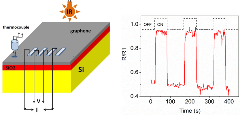
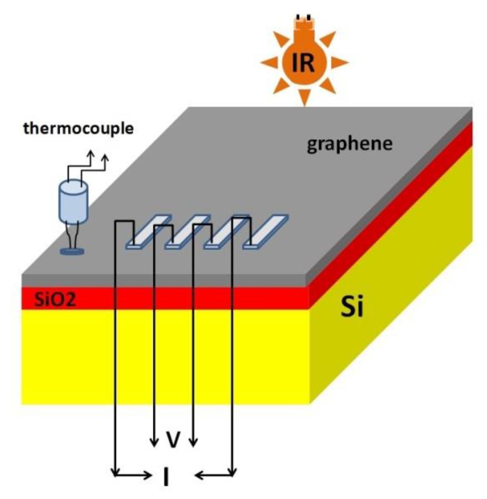
−1. Scanning electron microscopy (SEM) and high-resolution transmission electron microscopy (HRTEM) were carried out in the Jeol-6390 (Jeol, Pleasanton, CA, USA) and JSM-2010F (Jeol, Pleasanton, CA, USA) setups. The bolometric measurements were done on the VAG graphene film at room temperature (293 K). The schematic diagram of the experimental setup for the bolometric measurements is shown in
Figure 1. Silver paste was used to improve the contact of the probes with the VAG. We used a 200 W IR Philips lamp to irradiate the VAG, which was placed at a distance of 30 cm from the top of the sample. The incident IR radiation power on the sample was ~6 mW/mm
2 and was measured by a calorimetric technique. We used a Cr–Al thermocouple to measure the real-time temperature of the VAG sample. The thermocouple was directly in contact with the VAG instead of being placed in the sample base, and we carried out simultaneous measurements of the resistance change and the temperature response of the VAG.
3. Results and Discussion
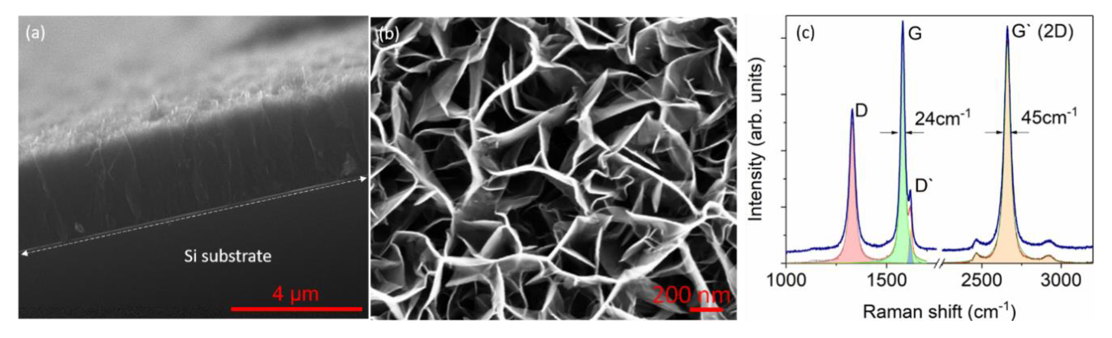
Figure 2a shows the SEM images of the grown VAG samples. It is evident that the samples were vertically aligned and the graphene platelets had a curved structure and intercalated randomly to form a mesh-like network. The size of the platelets varied from ~100 nm to ~2 μm. The platelet tip consisted of 5–10 layers of graphene, while the base of the platelet was thicker, perhaps consisting of 10–20 layers [
26,
27,
28,
29]. These nanoflakes were essentially vertically stacked two-dimensional graphene sheets growing from the underlying substrate and terminating into open graphitic-edge planes. Previous characterizations including electron microscopy, X-ray diffraction and Raman spectroscopy have conclusively proved that the synthesized structures are made up of highly graphitized sheets with a few layers of graphene on the edges. An in-depth explanation of the structure and the corresponding growth mechanism can be found in our earlier works [
26,
27,
28,
29]. This unique morphology is a cumulative effect of the internal stress-inducing factors and electrical self-bias field which is imposed on the substrate surface from the plasma environment [
30,
31]. The advantage of such a vertical architecture of graphene, particularly in opto-electronic applications, is that the effective surface area is superior throughout all directions of incident radiation on the VGA film, which in turn offers a higher absorption of the radiation when compared with a graphene film with planar architecture.
The typical Raman spectra of graphene and few-layered graphene-like systems exhibit at least three to four major bands, denoted as D (~1330 cm
−1), G (~1580 cm
−1), D′ (~1620 cm
−1) and G′ (~2660 cm
−1) [
26,
27,
28,
29,
30,
31]. As seen in
Figure 2c, all these bands were clearly distinguished and observed for the VAG samples. The Raman spectra were further analyzed for their band shape and full-width at half-maximum (FWHM) parameters, in accordance with our previous work, using Lorentzian peak shapes for D, G and G′ (2D) bands, and a Gaussian peak for the D′ band [
26,
27,
28,
29,
30,
31]. While the low FWHM (~25 cm
−1) of the G band is indicative of a high degree of graphitisation, the narrow FWHM of the G′ (2D) band along with the absence of a graphitic shoulder is further confirmed as one of the indicators of a few-layered graphene (FLG) system (
Figure 2) [
28,
29,
30,
31]. In our studies, the FWHM of the G′ band was around 43.3 cm
−1, lying within the range of 35–50 cm
−1 observed for few-layered graphene systems [
26,
27,
28,
29,
30,
31]. For the qualitative analysis of carbon nanostructures, the value of I
D/I
G is considered as the quality factor and ideally, for highly oriented pyrolytic graphite (HOPG), this value should be zero. For FLG nanoflakes, the value of I
D/I
G obtained was around 0.65. Since the graphene platelets are vertically aligned in nature, the Raman signal mostly originates from the edges of the graphene, which could be the reason for such an intense 2D peak in the Raman spectrum. The apparent high value of I
D/I
G is caused by the high density of flakes and associated large number of edges which predominantly contribute towards the rise of the defect peak [
30,
31].
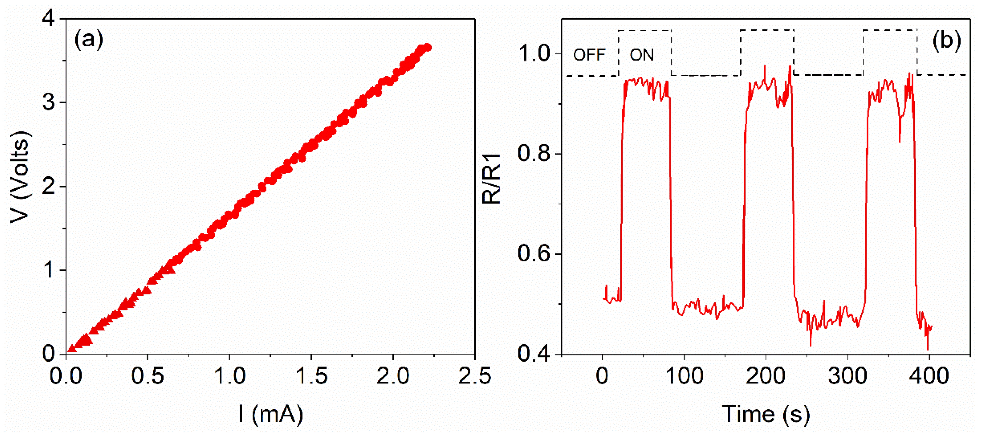
In
Figure 3, the current–voltage (I–V) characteristics of the sample in normal conditions (at 293 K normal day light) and upon IR irradiation can be observed. Under normal conditions, the I–V curve shows highly linear characteristics, which confirms the existence of a perfect ohmic contact on the graphene sample, with no change occurring in the contact resistance values throughout the experiments (see
Figure 3a). The corresponding resistance recorded at the normal condition was ~1.8 KΩ.
To examine the photoresponse of the VAG sample, we measured the voltage response upon periodic irradiation of IR on the sample at a constant current (~2 mA) in the circuit.
Figure 3b shows the switching characteristic of the photoresponse due to periodic IR irradiation with a 60 s pulse and a 90 s interval. Such long duration pulses were kept to record the saturation and the baseline behavior of the response. When the IR was switched on the resistance increased rapidly to saturation, and when the IR was switched off, the resistance returned to baseline with a sharp drop. The plot shows that the baseline and the saturation line are almost parallel, indicating that the changes were solely due to photoexcitation and not to any change in contact resistance. The response time for the enhancement of the resistance from the baseline to saturation was ~5 s. Such a high response time and increase in resistance upon IR irradiation can occur only from a bolometric photoresponse [
8,
9,
32,
33,
34]. In the case of a photoresponse arising from excitons or from photoconductivity via the interband transition, the response time is expected to be much lower (range within 10
−9 to 10
−15 s), and more importantly, the resistance decreases upon IR irradiation [
34]. The normalized resistance
(
being the actual resistance, and
the maximum resistance during saturation) was enhanced—twofold in the bolometric measurement at room temperature, which is quite remarkable. The sensitivity of the bolometer is defined as
where
is the saturation resistance, and
is the base line resistance. In most of the previous reports on the photoresponse of CNT, this sensitivity (
) was measured to be within the range of 0.01% to 30%, even when measured at cryogenic temperatures [
1,
3,
4]. In contrast, in our case, it can be clearly noticed in
Figure 3b that the normalized resistance increased dramatically from its initial value of 0.5 to 0.96 at saturation, offering sensitivity (
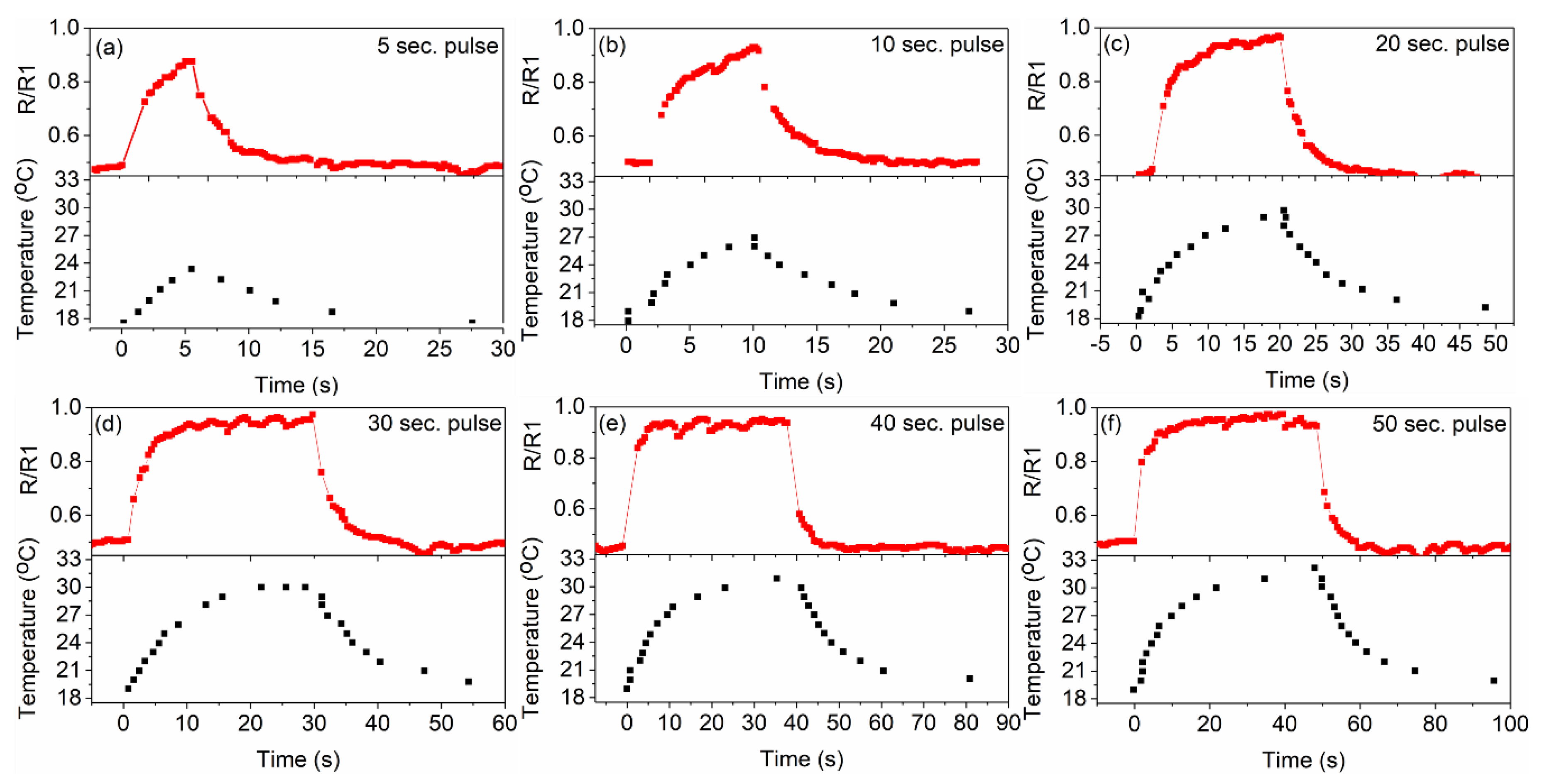
) ~92%, despite using a radiation power similar to that used in previous reports on the CNT bolometric response. Such a high range in resistance variation due to the bolometric response, can facilitate the detection of very small differences in temperature, which could be very useful for new-generation bolometric device applications. To further investigate the behavior of the bolometric photoresponse of the VAG samples, we recorded the resistance change occurring for different pulse durations (5 s, 10 s, 20 s, 30 s, 40 s and 50 s) of IR irradiation.
Figure 4 shows the changes in normalized resistance (
) for different pulse durations and the corresponding temperature of the VAG, measured by the thermocouple, which was directly in contact with the VAG surface. For the 5 s pulse, the normalized resistance just reached the saturation region, whereas for higher time duration pulses, the saturation regions were well established. It was found from each plot that the normalized resistance varied with time (t) exponentially during heating (Equation (2)) and cooling (Equation (3)) as:
where
and
are positive constants. Also with higher duration IR pulses (30 s onwards), it was clearly noticed that the resistance periodically fluctuated in the saturation region, which might be due to the periodic fluctuation of temperature at steady state. It was also noticed that during cooling, the normalized resistance of the VGA film did not regain its original resistance immediately, which was possibly due to the combined effect of capacitance within the graphene flakes and isothermal cooling. Such an effect was prominent for longer pulses and died out with time. It is quite clear from the figure that the resistance varied in a similar fashion to the temperature of the sample (i.e., reading from the thermocouple in contact with the sample surface), thereby confirming our argument that the photoresponse observed for these VAG samples was bolometric in nature. According to the thermocouple reading, the steady-state temperature was ~(31 ± 1) °C. The major difference between the temperature curve and the resistance curve was that the resistance curve approached saturation much faster than the temperature curve, indicating that the VAG bolometer has a higher response than the thermocouple.
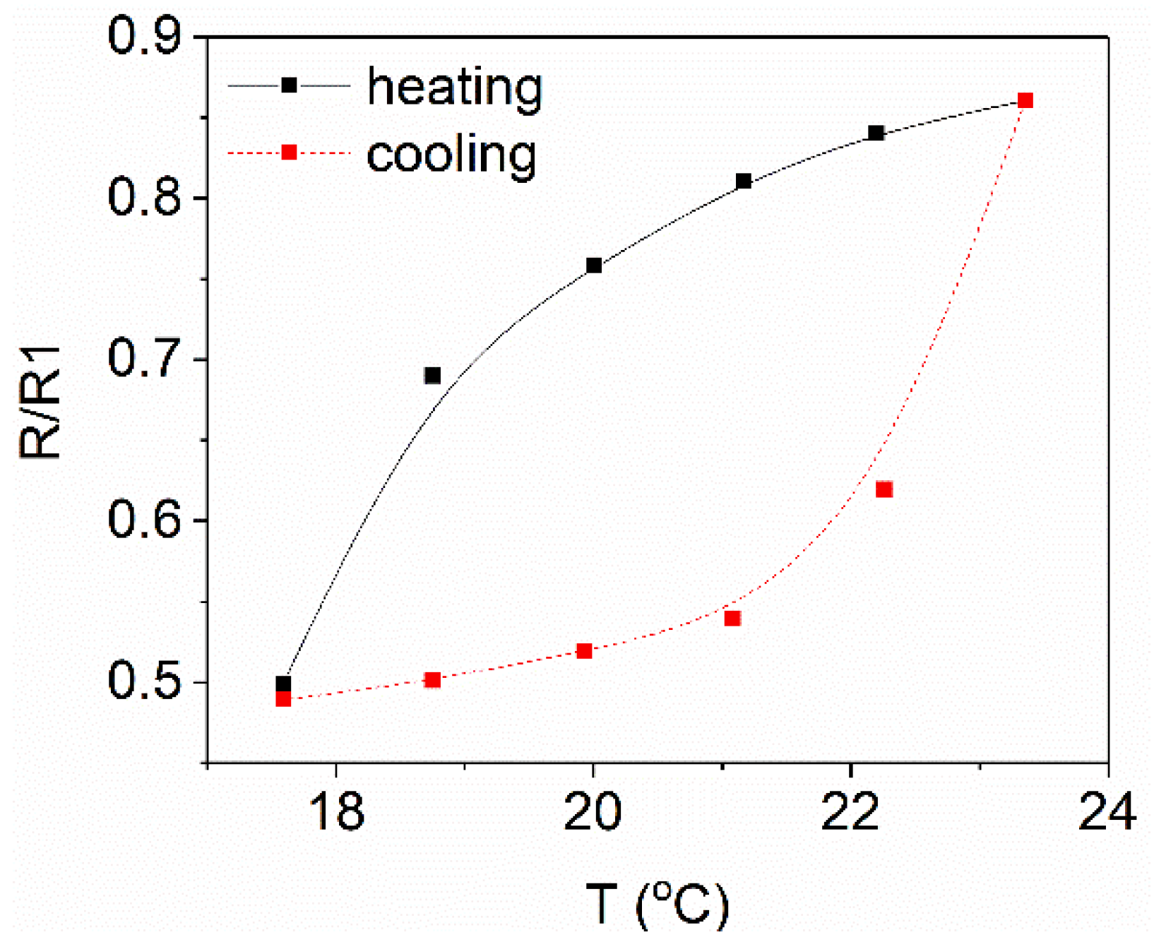
To get a clear view of the temperature dependence of the VAG resistance, we plotted the hysteresis loop (
Figure 5) of normalized resistance vs the thermocouple reading for the 5 s IR pulse. The 5 s pulse was chosen to avoid the steady-state saturation region and to get the response only during cooling and heating. At room temperature, both the heating and cooling curve showed a nonlinear response of resistance to temperature, although at a low temperature and for short-range temperature changes, the response could be considered linear. During heating, the normalised resistance rises rapidly when in the low-temperature region, however, as the temperature increases, the rate of increase becomes slower and approaches a steady-state following the exponential function:
where
= 0.87,
= 322,887,
= 0.63 and
is the temperature (in °C). The scenario reverses during the cooling and it obeys the function:
where
= 0.50,
= 8.9 × 10
−12 and
= 1.06. The rate of change in resistance with temperature (
) is positive for the heating curve and shows negative values for the cooling curve, which is expected for a bolometric photoresponse and is indicative of the metallic behavior of the VAGs. One of the most important parameters for measuring the bolometric response is the Thermal Coefficient of Resistance (TCR) which is defined as
and is the normalized change in resistance with temperature. Materials with a larger TCR are preferred for a bolometric application; for better responsivity, it is desirable to have a higher resistance change with a small change in temperature. TCR values were calculated from the simultaneous measurements of the temperature and resistance (
Figure 4) of the VGA film by a source meter and a thermocouple, as shown in the schematic of
Figure 1. The TCR of the VAG bolometer was calculated from the heating curve of the hysteresis loop; while temperature rose from 18 to 23 °C, the TCR was ~11%/K, significantly higher than in previous reports of TCR on MWNT with a number of layers <10, which showed a value in the range of 0.01–3%/K [
1,
3,
4].
TCR can show higher values for lower temperature ranges as the temperature moves away from the steady-state temperature and the slope of the heating curve increases. The high values of measured TCR for the VAG samples can be attributed to the higher effective surface area of the graphene when compared with the CNT. The graphene samples will have a higher flux of IR radiation, especially the VAG (due to their alignment), than the CNT. It could also be anticipated from previous reports [
1,
3] that the TCR could be improved further at a cryogenic temperature or by arranging thermal isolation through a vacuum for the VAG sample, which could pave a path towards the development of next-generation bolometric sensors.

 ,
, 
