
Horizontally Aligned Carbon Nanotube Based Biosensors for Protein Detection


Abstract
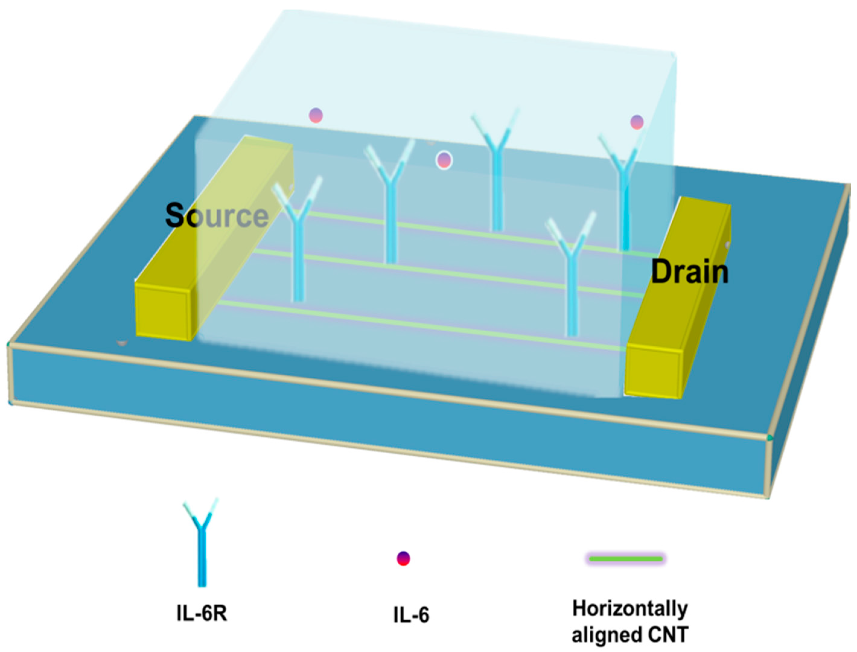
:1. Introduction
2. Experimental
2.1. Materials
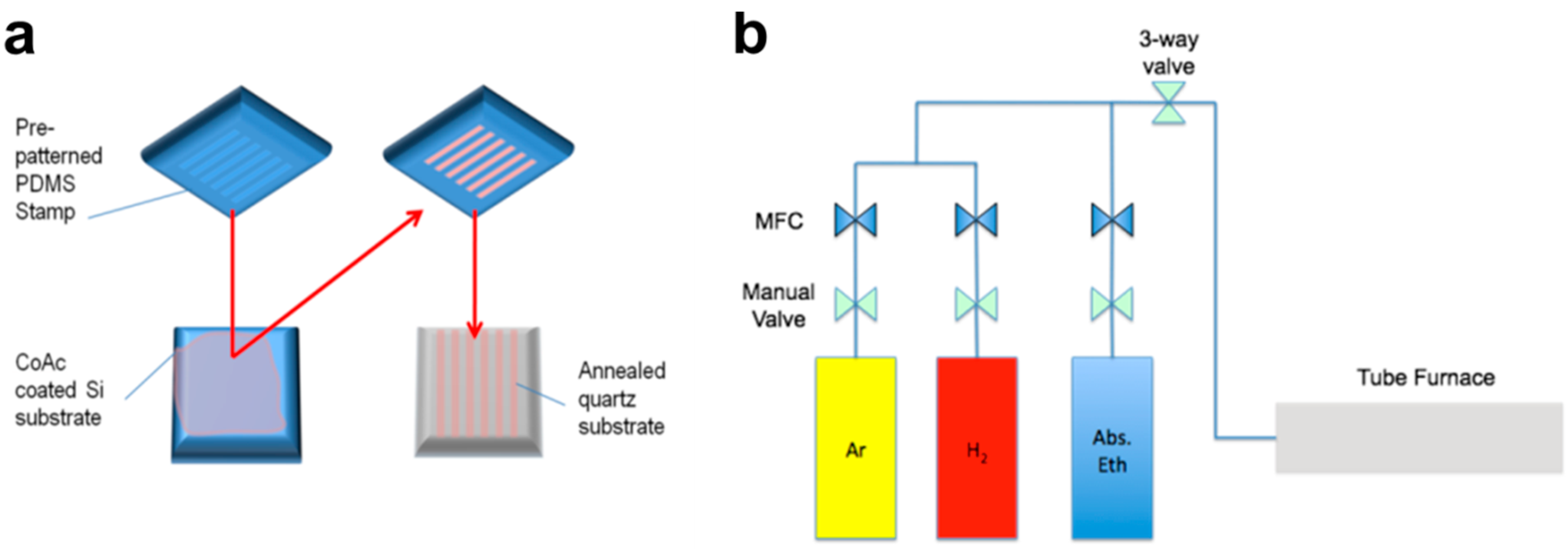
2.2. Methods
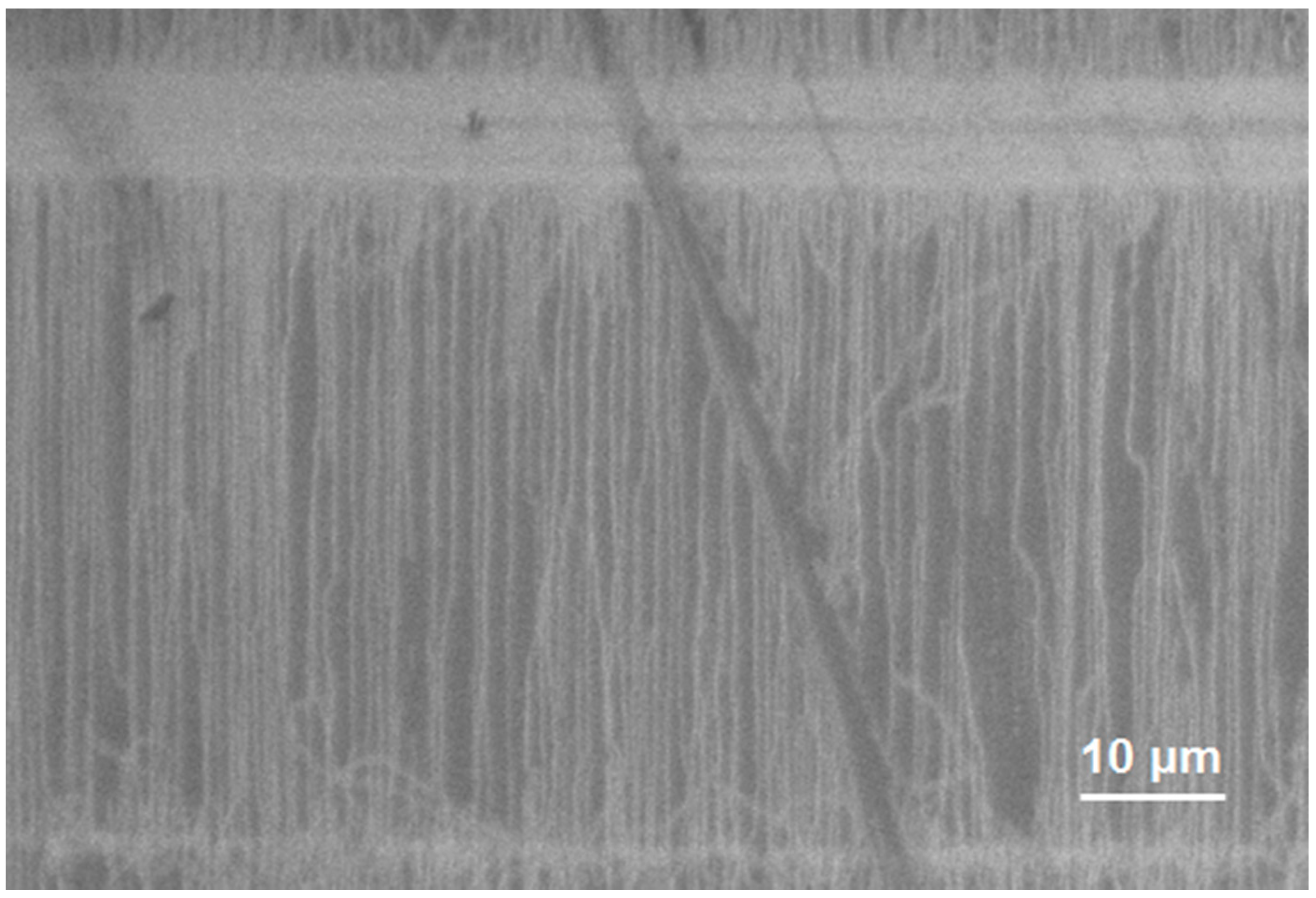
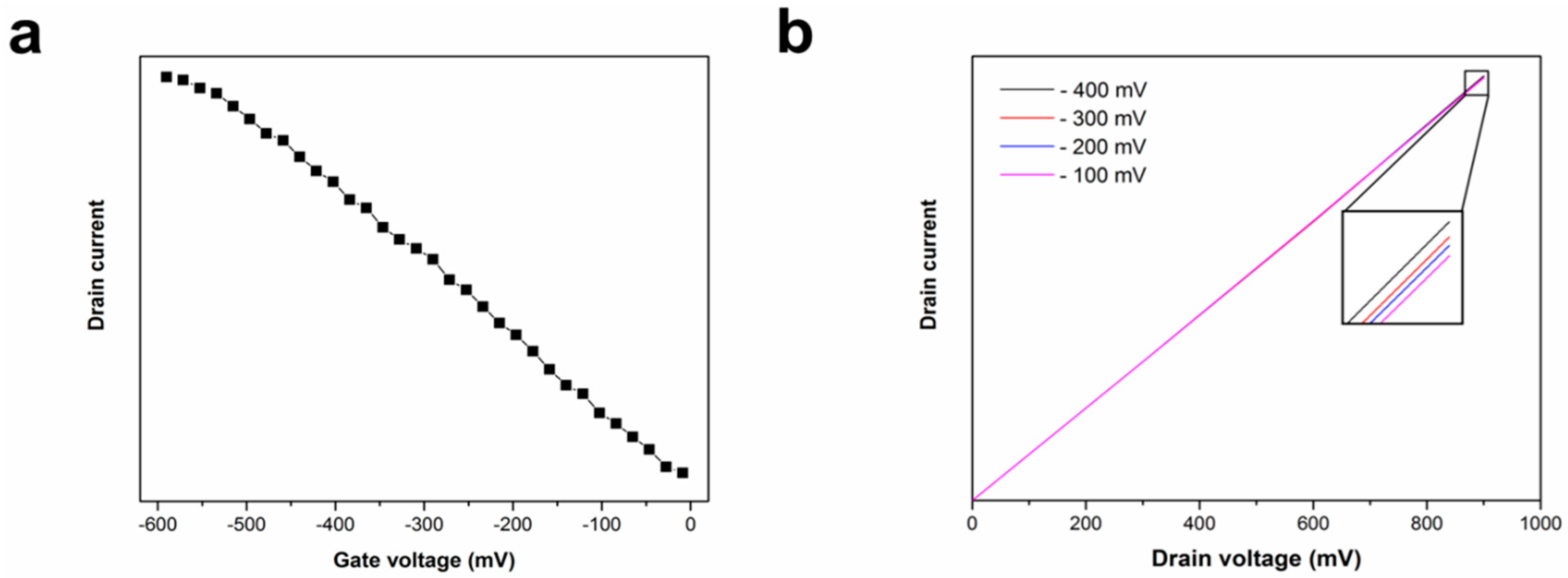
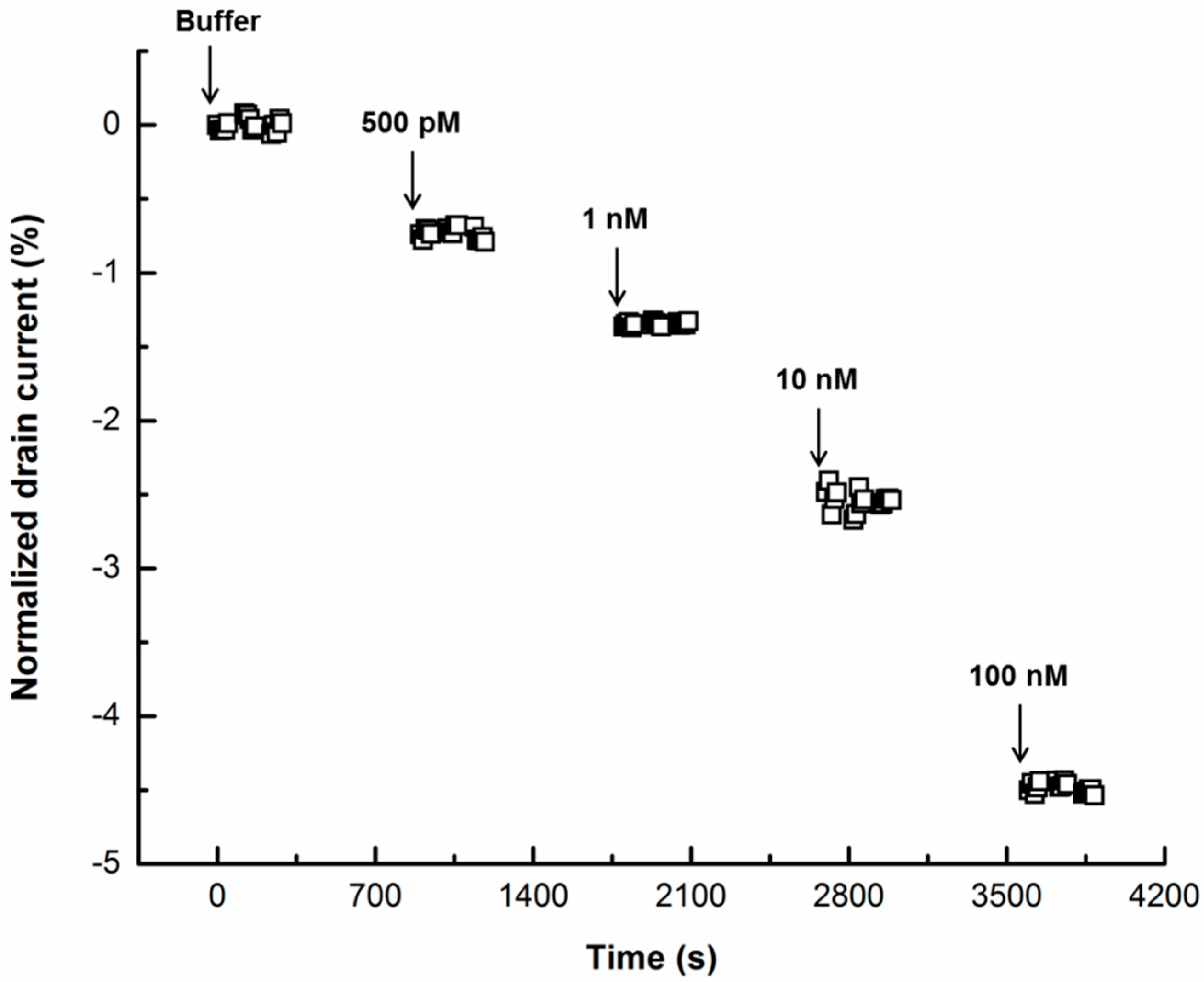
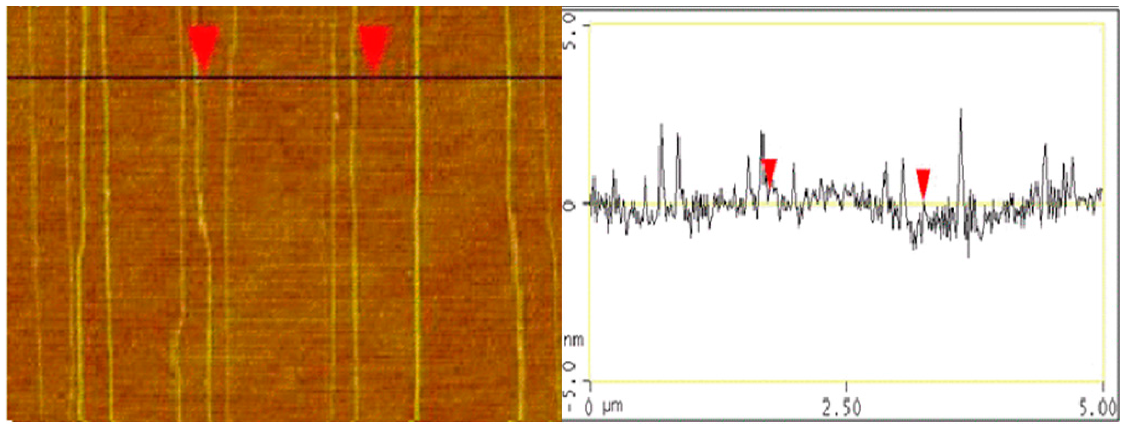
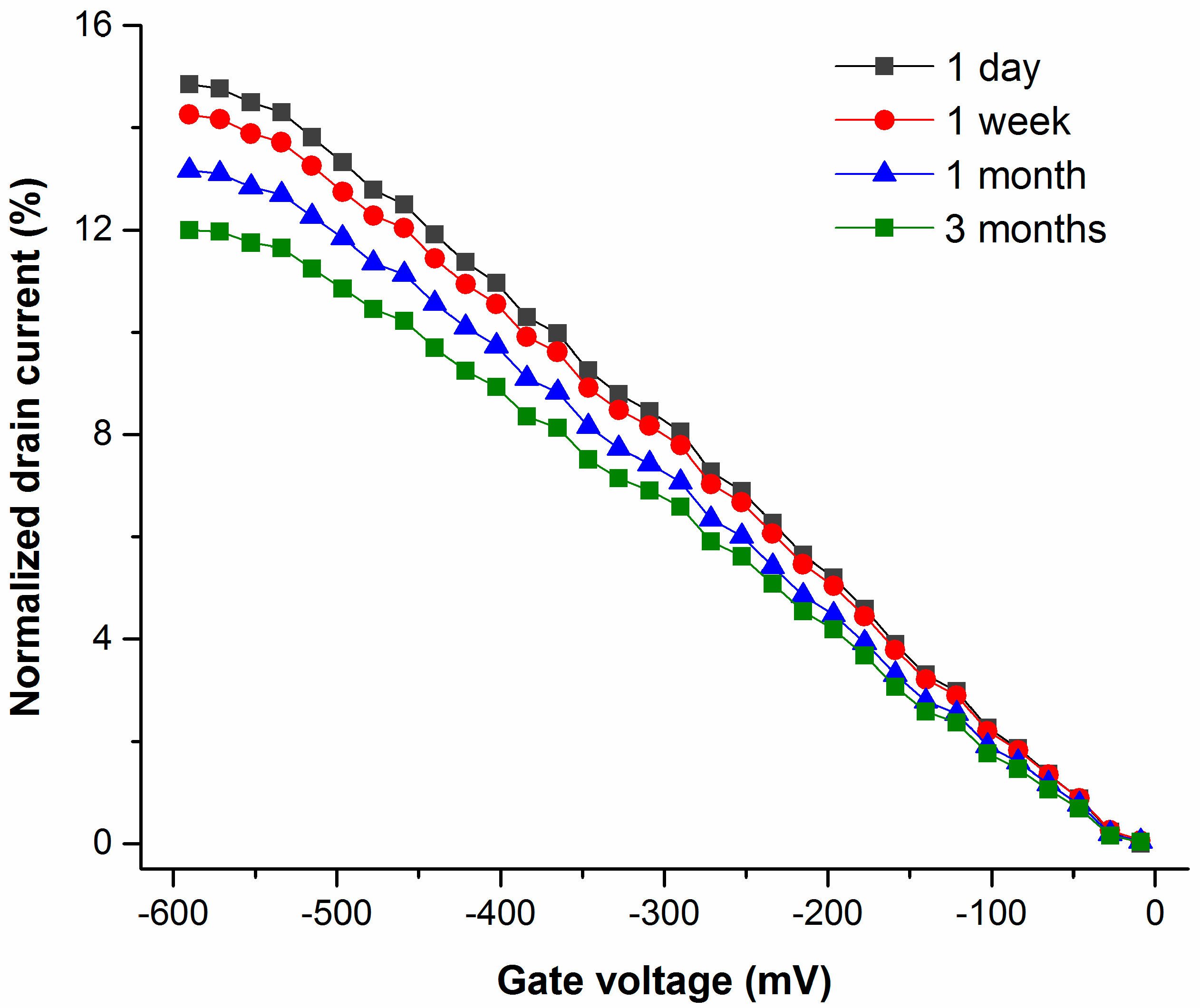
3. Results and Discussion
4. Conclusions
Supplementary Materials
Acknowledgments
Author Contributions
Conflicts of Interest
References
- Iijima, S. Helical microtubules of graphitic carbon. Nature 1991, 354, 56–58. [Google Scholar] [CrossRef]
- Yu, M.-F.; Files, B.S.; Arepalli, S.; Ruoff, R.S. Tensile loading of ropes of single wall carbon nanotubes and their mechanical properties. Phys. Rev. Lett. 2000, 84, 5552–5555. [Google Scholar] [CrossRef] [PubMed]
- Fam, D.W.H.; Palaniappan, A.; Tok, A.I.Y.; Liedberg, B.; Moochhala, S.M. A review on technological aspects influencing commercialization of carbon nanotube sensors. Sens. Actuators B Chem. 2011, 157, 1–7. [Google Scholar] [CrossRef]
- Ruoff, R.S.; Lorents, D.C. Mechanical and thermal properties of carbon nanotubes. Carbon 1995, 33, 925–930. [Google Scholar] [CrossRef]
- Zhu, L.; Xu, J.; Xiu, Y.; Sun, Y.; Hess, D.W.; Wong, C.P. Growth and electrical characterization of high-aspect-ratio carbon nanotube arrays. Carbon 2006, 44, 253–258. [Google Scholar] [CrossRef]
- Dürkop, T.; Getty, S.A.; Cobas, E.; Fuhrer, M.S. Extraordinary mobility in semiconducting carbon nanotubes. Nano Lett. 2004, 4, 35–39. [Google Scholar] [CrossRef]
- Saito, R.; Dresselhaus, G.; Dresselhaus, M.S. Physical Properties of Carbon Nanotubes; World Scientific: Singapore, 1998; Volume 35. [Google Scholar]
- Iijima, S.; Ichihashi, T. Single-shell carbon nanotubes of 1-nm diameter. Nature 1993, 363, 603–605. [Google Scholar] [CrossRef]
- Bethune, D.S.; Klang, C.H.; de Vries, M.S.; Gorman, G.; Savoy, R.; Vazquez, J.; Beyers, R. Cobalt-catalysed growth of carbon nanotubes with single-atomic-layer walls. Nature 1993, 363, 605–607. [Google Scholar] [CrossRef]
- Ebbesen, T.W.; Ajayan, P.M. Large-scale synthesis of carbon nanotubes. Nature 1992, 358, 220–222. [Google Scholar] [CrossRef]
- Thess, A.; Lee, R.; Nikolaev, P.; Dai, H. Crystalline ropes of metallic carbon nanotubes. Science 1996, 273, 483–487. [Google Scholar] [CrossRef] [PubMed]
- Hsieh, S.-H.; Horng, J.-J.; Tsai, C.-K. Growth of carbon nanotube on micro-sized Al2O3 particle and its application to adsorption of metal ions. J. Mater. Res. 2006, 21, 1269–1273. [Google Scholar] [CrossRef]
- José-Yacamán, M.; Miki-Yoshida, M.; Rendón, L.; Santiesteban, J.G. Catalytic growth of carbon microtubules with fullerene structure. Appl. Phys. Lett. 1993, 62, 202–204. [Google Scholar] [CrossRef]
- Li, W.; Xie, S.; Qian, L.; Chang, B. Large-scale synthesis of aligned carbon nanotubes. Science 1996, 274, 1701–1703. [Google Scholar] [CrossRef] [PubMed]
- Yah, C.S.; Iyuke, S.E.; Simate, G.S.; Unuabonah, E.I.; Bathgate, G.; Matthews, G.; Cluett, J.D. Continuous synthesis of multiwalled carbon nanotubes from xylene using the swirled floating catalyst chemical vapor deposition technique. J. Mater. Res. 2011, 26, 640–644. [Google Scholar] [CrossRef]
- Chen, H.; Choo, T.K.; Huang, J.; Wang, Y.; Liu, Y.; Platt, M.; Palaniappan, A.; Liedberg, B.; Tok, A.I.Y. Label-free electronic detection of interleukin-6 using horizontally aligned carbon nanotubes. Mater. Des. 2016, 90, 852–857. [Google Scholar] [CrossRef]
- Ma, Y.; Wang, B.; Wu, Y.; Huang, Y.; Chen, Y. The production of horizontally aligned single-walled carbon nanotubes. Carbon 2011, 49, 4098–4110. [Google Scholar] [CrossRef]
- Martel, R.; Schmidt, T.; Shea, H.R.; Hertel, T.; Avouris, P. Single- and multi-wall carbon nanotube field-effect transistors. Appl. Phys. Lett. 1998, 73, 2447–2449. [Google Scholar] [CrossRef]
- Fam, D.W.H.; Azoubel, S.; Liu, L.; Huang, J.; Mandler, D.; Magdassi, S.; Tok, A.I.Y. Novel felt pseudocapacitor based on carbon nanotube/metal oxides. J. Mater. Sci. 2015, 50, 6578–6585. [Google Scholar] [CrossRef]
- Hsu, C.M.; Lin, C.H.; Chang, H.L.; Kuo, C.T. Growth of the large area horizontally-aligned carbon nanotubes by ECR-CVD. Thin Solid Films 2002, 420–421, 225–229. [Google Scholar] [CrossRef]
- Choi, G.S.; Cho, Y.S.; Hong, S.Y.; Park, J.B.; Son, K.H.; Kim, D.J. Carbon nanotubes synthesized by ni-assisted atmospheric pressure thermal chemical vapor deposition. J. Appl. Phys. 2002, 91, 3847–3854. [Google Scholar] [CrossRef]
- Giancane, G.; Ruland, A.; Sgobba, V.; Manno, D.; Serra, A.; Farinola, G.M.; Omar, O.H.; Guldi, D.M.; Valli, L. Aligning single-walled carbon nanotubes by means of langmuir–blodgett film deposition: Optical, morphological, and photo-electrochemical studies. Adv. Funct. Mater. 2010, 20, 2481–2488. [Google Scholar] [CrossRef]
- Chen, J.; Liu, Y.; Minett, A.I.; Lynam, C.; Wang, J.; Wallace, G.G. Flexible, aligned carbon nanotube/conducting polymer electrodes for a lithium-ion battery. Chem. Mater. 2007, 19, 3595–3597. [Google Scholar] [CrossRef]
- Palaniappan, A.; Goh, W.H.; Fam, D.W.H.; Rajaseger, G.; Chan, C.E.Z.; Hanson, B.J.; Moochhala, S.M.; Mhaisalkar, S.G.; Liedberg, B. Label-free electronic detection of bio-toxins using aligned carbon nanotubes. Biosens. Bioelectron. 2013, 43, 143–147. [Google Scholar] [CrossRef] [PubMed]
- Wujcik, E.K.; Wei, H.; Zhang, X.; Guo, J.; Yan, X.; Sutrave, N.; Wei, S.; Guo, Z. Antibody nanosensors: A detailed review. RSC Adv. 2014, 4, 43725–43745. [Google Scholar] [CrossRef]
- Kang, S.J.; Kocabas, C.; Ozel, T.; Shim, M.; Pimparkar, N.; Alam, M.A.; Rotkin, S.V.; Rogers, J.A. High-performance electronics using dense, perfectly aligned arrays of single-walled carbon nanotubes. Nat. Nanotechnol. 2007, 2, 230–236. [Google Scholar] [CrossRef] [PubMed]
- Esfandyarpour, R.; Esfandyarpour, H.; Javanmard, M.; Harris, J.S.; Davis, R.W. Microneedle biosensor: A method for direct label-free real time protein detection. Sens. Actuators B Chem. 2013, 177, 848–855. [Google Scholar] [CrossRef] [PubMed]
- Esfandyarpour, R.; Javanmard, M.; Koochak, Z.; Esfandyarpour, H.; Harris, J.S.; Davis, R.W. Label-free electronic probing of nucleic acids and proteins at the nanoscale using the nanoneedle biosensor. Biomicrofluidics 2013, 7, 044114. [Google Scholar] [CrossRef] [PubMed]
- Goda, T.; Miyahara, Y. Label-free and reagent-less protein biosensing using aptamer-modified extended-gate field-effect transistors. Biosens. Bioelectron. 2013, 45, 89–94. [Google Scholar] [CrossRef] [PubMed]
- Goda, T.; Tabata, M.; Sanjoh, M.; Uchimura, M.; Iwasaki, Y.; Miyahara, Y. Thiolated 2-methacryloyloxyethyl phosphorylcholine for an antifouling biosensor platform. Chem. Commun. 2013, 49, 8683–8685. [Google Scholar] [CrossRef] [PubMed]
- Kim, D.-J.; Sohn, I.Y.; Jung, J.-H.; Yoon, O.J.; Lee, N.E.; Park, J.-S. Reduced graphene oxide field-effect transistor for label-free femtomolar protein detection. Biosens. Bioelectron. 2013, 41, 621–626. [Google Scholar] [CrossRef] [PubMed]
- Kim, S.K.; Cho, H.; Park, H.-J.; Kwon, D.; Lee, J.M.; Chung, B.H. Nanogap biosensors for electrical and label-free detection of biomolecular interactions. Nanotechnology 2009, 20, 455502. [Google Scholar] [CrossRef] [PubMed]
- Balk, S.P.; Ko, Y.-J.; Bubley, G.J. Biology of prostate-specific antigen. J. Clin. Oncol. 2003, 21, 383–391. [Google Scholar] [CrossRef] [PubMed]
- Catalona, W.J.; Richie, J.P.; Ahmann, F.R.; Hudson, M.A.; Scardino, P.T.; Flanigan, R.C.; deKernion, J.B.; Ratliff, T.L.; Kavoussi, L.R.; Dalkin, B.L. Comparison of digital rectal examination and serum prostate specific antigen in the early detection of prostate cancer: Results of a multicenter clinical trial of 6630 men. J. Urol. 1994, 151, 1283–1290. [Google Scholar] [PubMed]
- Stamey, T.A.; Yang, N.; Hay, A.R.; McNeal, J.E.; Freiha, F.S.; Redwine, E. Prostate-specific antigen as a serum marker for adenocarcinoma of the prostate. N. Engl. J. Med. 1987, 317, 909–916. [Google Scholar] [CrossRef] [PubMed]
- Gao, N.; Zhou, W.; Jiang, X.; Hong, G.; Fu, T.-M.; Lieber, C.M. General strategy for biodetection in high ionic strength solutions using transistor-based nanoelectronic sensors. Nano Lett. 2015, 15, 2143–2148. [Google Scholar] [CrossRef] [PubMed]
- Thompson, I.M.; Pauler, D.K.; Goodman, P.J.; Tangen, C.M.; Lucia, M.S.; Parnes, H.L.; Minasian, L.M.; Ford, L.G.; Lippman, S.M.; Crawford, E.D.; et al. Prevalence of prostate cancer among men with a prostate-specific antigen level ≤4.0 ng per milliliter. N. Engl. J. Med. 2004, 350, 2239–2246. [Google Scholar] [CrossRef] [PubMed]
- Chen, H.; Chen, P.; Huang, J.; Selegård, R.; Platt, M.; Palaniappan, A.; Aili, D.; Tok, A.I.Y.; Liedberg, B. Detection of matrilysin activity using polypeptide functionalized reduced graphene oxide field-effect transistor sensor. Anal. Chem. 2016, 88, 2994–2998. [Google Scholar] [CrossRef] [PubMed]
- Huang, L.; Cui, X.; White, B.; O’Brien, S.P. Long and oriented single-walled carbon nanotubes grown by ethanol chemical vapor deposition. J. Phys. Chem. B 2004, 108, 16451–16456. [Google Scholar] [CrossRef]
- Krüger, M.; Buitelaar, M.R.; Nussbaumer, T.; Schönenberger, C.; Forró, L. Electrochemical carbon nanotube field-effect transistor. Appl. Phys. Lett. 2001, 78, 1291–1293. [Google Scholar] [CrossRef]
- Chen, R.J.; Zhang, Y.; Wang, D.; Dai, H. Noncovalent sidewall functionalization of single-walled carbon nanotubes for protein immobilization. J. Am. Chem. Soc. 2001, 123, 3838–3839. [Google Scholar] [CrossRef] [PubMed]
- Kocabas, C.; Kang, S.J.; Ozel, T.; Shim, M.; Rogers, J.A. Improved synthesis of aligned arrays of single-walled carbon nanotubes and their implementation in thin film type transistors. J. Phys. Chem. C 2007, 111, 17879–17886. [Google Scholar] [CrossRef]
- Palaniappan, A.; Goh, W.H.; Tey, J.N.; Wijaya, I.P.M.; Moochhala, S.M.; Liedberg, B.; Mhaisalkar, S.G. Aligned carbon nanotubes on quartz substrate for liquid gated biosensing. Biosens. Bioelectron. 2010, 25, 1989–1993. [Google Scholar] [CrossRef] [PubMed]
- Kojima, A.; Hyon, C.K.; Kamimura, T.; Maeda, M.; Matsumoto, K. Protein sensor using carbon nanotube field effect transistor. Jpn. J. Appl. Phys. 2005, 44, 1596–1598. [Google Scholar] [CrossRef]
- Villoutreix, B.O.; Griffin, J.H.; Getzoff, E.D. A structural model for the prostate disease marker, human prostate-specific antigen. Protein Sci. 1994, 3, 2033–2044. [Google Scholar] [CrossRef] [PubMed]
- Heller, I.; Janssens, A.M.; Männik, J.; Minot, E.D.; Lemay, S.G.; Dekker, C. Identifying the mechanism of biosensing with carbon nanotube transistors. Nano Lett. 2008, 8, 591–595. [Google Scholar] [CrossRef] [PubMed]
- Torsi, L.; Farinola, G.M.; Marinelli, F.; Tanese, M.C.; Omar, O.H.; Valli, L.; Babudri, F.; Palmisano, F.; Zambonin, P.G.; Naso, F. A sensitivity-enhanced field-effect chiral sensor. Nat. Mat. 2008, 7, 412–417. [Google Scholar] [CrossRef] [PubMed]
- Chen, H.; Lim, S.K.; Chen, P.; Huang, J.; Wang, Y.; Palaniappan, A.; Platt, M.; Liedberg, B.; Tok, A.I.Y. Reporter-encapsulated liposomes on graphene field effect transistors for signal enhanced detection of physiological enzymes. Phys. Chem. Chem. Phys. 2015, 17, 3451–3456. [Google Scholar] [CrossRef] [PubMed]


© 2016 by the authors; licensee MDPI, Basel, Switzerland. This article is an open access article distributed under the terms and conditions of the Creative Commons Attribution (CC-BY) license (http://creativecommons.org/licenses/by/4.0/).
Share and Cite
Chen, H.; Huang, J.; Fam, D.W.H.; Tok, A.I.Y. Horizontally Aligned Carbon Nanotube Based Biosensors for Protein Detection. Bioengineering 2016, 3, 23. https://doi.org/10.3390/bioengineering3040023
Chen H, Huang J, Fam DWH, Tok AIY. Horizontally Aligned Carbon Nanotube Based Biosensors for Protein Detection. Bioengineering. 2016; 3(4):23. https://doi.org/10.3390/bioengineering3040023
Chicago/Turabian StyleChen, Hu, Jingfeng Huang, Derrick Wen Hui Fam, and Alfred Iing Yoong Tok. 2016. "Horizontally Aligned Carbon Nanotube Based Biosensors for Protein Detection" Bioengineering 3, no. 4: 23. https://doi.org/10.3390/bioengineering3040023
APA StyleChen, H., Huang, J., Fam, D. W. H., & Tok, A. I. Y. (2016). Horizontally Aligned Carbon Nanotube Based Biosensors for Protein Detection. Bioengineering, 3(4), 23. https://doi.org/10.3390/bioengineering3040023