Article

Microwave-Mediated Extraction of Critical Metals from LED E-Waste

by
Athanasios B. Bourlinos
1,*,
Christina Papachristodoulou
1,
Anastasios Markou
1,
Nikolaos Chalmpes
2,*,
Emmanuel P. Giannelis
2,
Dimitrios P. Gournis
3,4,
Constantinos E. Salmas
5 and
Michael A. Karakassides
5,*
1
Physics Department, University of Ioannina, 45110 Ioannina, Greece
2
Department of Materials Science & Engineering, Cornell University, Ithaca, NY 14850, USA
3
School of Chemical & Environmental Engineering, Technical University of Crete, 73100 Chania, Greece
4
Institute of GeoEnergy, Foundation for Research & Technology-Hellas, 73100 Chania, Greece
5
Department of Materials Science & Engineering, University of Ioannina, 45110 Ioannina, Greece
*
Authors to whom correspondence should be addressed.
ChemEngineering 2025, 9(3), 47; https://doi.org/10.3390/chemengineering9030047
Submission received: 26 February 2025 / Revised: 12 April 2025 / Accepted: 21 April 2025 / Published: 29 April 2025

Abstract

This study introduces a microwave-assisted technique for extracting critical minerals from LED electronic waste. The process begins with microwave irradiation, which thermally decomposes the LED’s plastic lens into a brittle, charred residue. During this stage, the LED chip undergoes deflagration—being rapidly ejected from the reflective cavity and becoming embedded within the decomposed lens material. Consequently, the chip is encapsulated in the resulting charred residue. This composite, consisting of the charred lens and the LED chip, can be easily separated from the metallic pins (Fe, Ni, Ag), which remain almost undamaged. Subsequent calcination of the charred material in air exposes the materials making up the LED chip, which contain critical metals (e.g., Ga, As, In, Y, Au). These metals are then extracted through a two-step acid leaching process involving aqua regia followed by hot concentrated hydrochloric acid, yielding them in potentially recoverable forms. The synergistic effect of microwave irradiation and acid treatment achieves an average extraction efficiency of 96% for critical metals. Notably, this approach enables complete and loss-free recovery of the LED chip, offering a practical and efficient solution for LED e-waste recycling.

Graphical Abstract

1. Introduction

Light-emitting diodes (LEDs) are light sources based on a semiconducting LED chip and constructed of two pins (a cathode and an anode), a reflectivity cavity, a gold wiring, and a plastic lens that covers the device (Figure 1). When a voltage is applied, the device emits light, with the color dictated by the band gap of the semiconductor material used. LEDs represent an environmentally responsible and sustainable lighting technology offering significant advantages over traditional incandescent and fluorescent bulbs in terms of energy efficiency, lifespan, and environmental impact [1,2]. Compared to incandescent bulbs, LEDs consume up to 80% less electricity while providing equivalent brightness, thereby reducing overall energy consumption and associated greenhouse gas emissions from power generation—ultimately contributing to lower carbon footprints. With a typical operational lifespan ranging from 25,000 to 50,000 h, LEDs outperform conventional bulbs, which typically have a lifespan of around 1000 h. This extended durability leads to fewer replacements, reduced waste, and decreased manufacturing demand—key elements in promoting a circular economy. Unlike fluorescent lights, LEDs are mercury-free, eliminating concerns over toxic material handling and disposal. Their adaptability also supports integration into smart and renewable systems, such as motion-activated lighting and solar-powered streetlights, further supporting energy efficiency and the development of sustainable infrastructure.
While LEDs have not yet been officially classified as electronic waste (e-waste), manufacturers proactively advise proper disposal. Although, currently, there is not a strong impetus to recycle LEDs, that might change shortly because of the following. Firstly, consumers may replace LEDs sooner and before they cease to work due to rapid technological developments towards better performance at a lower cost. As a result, consumers may consider purchasing LED lights in the same way they do other electronic devices, replacing them well before their lifetime expires. This market trend is predicted to significantly increase LED production as well as LED waste in the environment. Secondly, LEDs are manufactured using a number of metals, including the more common iron and copper but also more valuable ones, such as aluminum, silver, gold, and more importantly gallium, arsenic, and indium among others. As the rates of production and use increase, critical metals like gallium, arsenic, and indium used in semiconductor manufacturing could be depleted within the next two decades. Based on the above reasoning, regulators and other government agencies are expected to introduce LED recycling programs to both reduce the environmental impact of LED waste and preserve the supply of critical metals essential for semiconductor manufacturing [3,4,5,6,7].
Current LED recycling methods include manual segregation, solvent dissolution, acid leaching, thermal treatment, or combinations thereof. Manual segregation typically involves mechanical processes such as prying, cutting, and cracking to separate the various components of the device [8,9]. Dissolution employs solvents that dissolve some materials [10,11], while leaching uses acids to extract valuable metals from the LED components [7,12,13,14,15]. Thermal treatment, on the other hand, involves heating to high temperatures to facilitate decomposition followed by separation [9,12,16,17]. Despite the effectiveness of these techniques, separating the LED components is often a labor-intensive and complex process that can jeopardize the benefits of recycling. The intricate structure of LEDs, which integrates multiple materials in compact designs, adds to the challenge of efficient disassembly and recovery. Given these challenges, researchers are actively searching for new simpler methods for recycling LEDs.
Microwave treatment of e-waste has emerged as a fast and eco-friendly method, particularly suitable for recycling e-waste that contains both plastics and metals, including printed circuit boards, cell phones, CDs, and copper cable wires. Microwave irradiation selectively heats the metal due to its high conductivity, while the surrounding plastic undergoes pyrolysis, breaking down into gasses, oils, and char. As the metal heats up during microwave treatment, it loosens up from the plastic matrix, enabling easy separation and recovery. Hence, this process has been explored for several applications, including metal recovery from e-waste [18,19,20,21,22,23,24,25,26,27]. However, no studies have reported the use of microwave technology for processing LED e-waste to date [23,24].
Herein, a microwave-assisted method is demonstrated for the first time, for extracting critical and valuable metals from LED e-waste. Microwave irradiation induces rapid deflagration of the LED chip from its reflective cavity, enabling efficient separation of components in a process in under a minute. This approach significantly reduces reliance on labor-intensive manual dismantling and minimizes the use of solvents or harsh chemicals. Following separation, a two-step acid treatment is applied to leach the metals out of the LED chip, achieving up to 96% efficiency and offering strong potential for metal recovery. Furthermore, the process is well-suited for batch processing, indicating its potential for large-scale implementation. Microwave-assisted separation thus holds significant promise for LED recycling, where speed and efficiency are crucial.

2. Materials and Methods

All chemicals and solvents were purchased from Sigma-Aldrich, St. Louis, MO, USA. Experiments were conducted using a household microwave oven (frequency 2.45 GHz, wavelength ca. 12 cm, diameter of protective net 2 mm). Microwave irradiation of plastic lenses leads to charring and the release of toxic gasses. To ensure safety, it is strongly advisable to conduct experiments in a well-ventilated area or under a fume hood. LEDs of various colors—white, warm, red, pink, orange, yellow, green, and blue—were employed (5 mm round T-1¾). The LEDs, each measuring 3 cm in size, were composed of three primary components: a plastic lens, an LED chip, and metallic pins (Figure 1).

2.1. Microwave-Mediated Processing of LED E-Waste

For the process, 10 to 20 LEDs were placed in a silica ceramic crucible (outer diameter: 5.8 cm) and subjected to irradiation in a household microwave oven at 700 W under ambient air while rotating for 1 min. This microwave treatment resulted in the charring of the plastic lenses, which encapsulate the LED chip, while leaving the metallic pins intact (length: 2.5–3.0 cm). Subsequent mechanical separation of the components involved hand scraping to detach the charred plastic lenses followed by magnetic separation using a hand magnet to remove the metallic pins. The recovered metallic pins, referred to as PNLED, were both attracted by a magnet and they were conductive. At this stage, there is no need to destroy the pins by acid dissolution in order to selectively recover their constituents, as they remain almost undamaged and could potentially be reused or re-purposed. The charred plastic residue (2.5 g from 400 LEDs) was further treated by calcination in air at 800 °C for 1 h, resulting in its complete removal from the chip, which is referred to as SMLED. Since the amount of SMLED is 0.1 mg per LED, approximately 400 LEDs were processed, in order to collect sufficient SMLED material (40 mg from 400 LEDs). The above process is illustrated in Figure 2. It should be mentioned that the microwave treatment utilized a power setting of 700 W, with an exposure time that proves adequate for achieving rapid and effective charring of the plastic lens with simultaneous deflagration of the LED chip. Reducing either the duration or the power fails to produce this desired effect.

2.2. Acid Treatment of the Recovered LED Chips

The extraction of various metals from SMLED was investigated through a two-stage method (Figure 2, flowchart). Initially, SMLED underwent acid treatment with aqua regia (40 mg per 2 mL of acid) at room temperature for 24 h. The leftover material was then calcined at 800 °C in air to improve its crystallinity. In the following step, the resulting crystalline solid (SMLEDH) was subjected to treatment with hot concentrated HCl (27 mg per 2 mL of acid) at 100 °C for 2 h to leave 1.5 mg residue (SMLEDHH).
Regarding the acid concentration, a high level is essential due to the highly insoluble and refractive nature of the materials composing the LED chip, necessitating the use of concentrated acids to ensure an efficient leaching process. Furthermore, the duration of the acid treatment aligns with timelines reported in similar studies within the literature. This approach enables a metal extraction efficiency of 96%, as evidenced by the minimal residual solid left (1.5 mg) from an initial 40 mg LED chip sample, indicating that the vast majority of the material is successfully leached out and thus potentially recoverable during the process.

2.3. Characterizations

The structure and elemental composition of all samples were studied using complementary X-ray diffraction (XRD) and X-ray fluorescence (XRF) techniques. XRD patterns were obtained using a glass holder (for pins) or a background-free silicon wafer (for powders) with Cu Kα radiation (λ = 1.54 Å) from a Bruker Advance D8 diffractometer (Bruker AXS Inc, Karlsruhe, Germany). Samples were scanned from 2 to 80° 2θ, in steps of 0.02° (2θ), at a rate of 0.2 s per step. Elemental analyses were carried out using a home-built Energy-Dispersive XRF spectrometer. Photons emitted from an annular 241Am source were used for sample excitation, while a Si (Li) crystal was used for the detection of fluorescent X-rays. Spectral analysis was carried out using the WinQxas software package (version 1.3) developed by the International Atomic Energy Agency (IAEA, Vienna, Austria). Metallic pins were analyzed directly with no sample pretreatment. Quantitative analysis was performed using a custom fundamental parameters code developed specifically for the spectrometer. Powder samples were measured in the form of 1.25 cm-diameter pellets, prepared by mixing certain amount of finely ground sample with microcrystalline cellulose. Elemental quantification was based on calibration curves obtained for each analyte from sets of standard pellets prepared by mixing high-purity reagents with microcrystalline cellulose. Electrical resistivity measurements were carried out on the LED pins using a four-point probe method. A Keithley 227 (Tektronix, Inc., Beaverton, OR, USA) current source was used to supply direct currents (DC), and the resulting voltage signals were detected using a Keithley 2010 multimeter from Tektronix (Tektronix, Inc., Beaverton, OR, USA).

3. Results and Discussion

3.1. Microwave Separation Mechanism and Materials Characterization

The presence of metallic pins in LEDs plays a crucial role in the microwave-assisted recovery process due to their high electrical conductivity. These pins rapidly absorb microwave energy and heat up, initiating the thermal decomposition necessary for material separation. Additionally, the physical dimensions of the LED being one-fourth of the microwave’s standing wave wavelength aligns with the peak of highest intensity in the wave (Figure 3A). This resonance enhances the interaction between the microwaves and the LED, amplifying the heating and separation dynamics [25,28]. This intense localized heating causes thermal expansion of the metallic pins (PNLED), weakening their bond with the surrounding plastic lens and, thus, facilitating mechanical separation. The plastic lens deteriorates into a brittle char under the high temperatures generated by the microwaves (Figure 3B), further softening the bonds and making the mechanical separation easier. During the initial stages of the microwave exposure, the LED chip deflagrates, leaving the pin’s cavity empty (Figure 3C,D). The brittle char encases the LED chip, allowing for easy separation from the metallic pin’s reflective cavity. Following this process, the charred residue is subjected to calcination in air, exposing SMLED material. The resulting materials (PNLED and SMLED) are analyzed using complementary X-ray techniques-XRD for structural characterization and XRF to determine the elemental composition of the samples.
The XRD pattern of PNLED reveals characteristic reflections corresponding to the silver coating, as shown on the left in Figure 4. This confirms the presence of a silver layer on the surface of the pins. Complementary XRF analysis identifies additional elements (Figure 4 (right) and Table 1), notably iron and nickel, which are barely seen in the XRD pattern. Among the latter, iron is present in a larger fraction in consistence with the observed magnetic properties of the metallic pins. The silver coating, on the other hand, accounts for the excellent conductivity of the pins. This combination of structural and compositional information illustrates the dual functionality of the metallic pins, with the iron core imparting magnetic behavior and the silver coating ensuring better conductivity. The magnetic properties of iron are not a critical factor in LED performance but may provide indirect benefits, such as electromagnetic compatibility in circuits and easy magnetic mounting and alignment of LED components. However, the primary reason for using iron in LEDs is its cost, as it is relatively inexpensive and readily available, making it a practical choice for manufacturers. Conductivity measurements using the four-point probe method showed that the pins exhibited a conductivity of 5.24 × 10⁶ S·m⁻1 prior to microwave heating, which is comparable to that of carbon steel (6.99 × 10⁶ S·m⁻1). After treatment, this value decreased by an order of magnitude to 4.95 × 10⁵ S·m⁻1, indicating that the pins largely retained their conductive nature.
The detection of mainly silver in the XRD pattern is due to the nature of the coating. According to the manufacturer’s specifications for the 5 mm round (T-1¾) LED utilized in this study, the pins feature a silver coating typically ranging from 2 to 3 μm in thickness, which is deposited over a nickel underlayer on a steel (Fe) base. The silver coating is sufficiently thick to attenuate the impinging Cu Kα X-ray beam by approximately 70% before reaching the nickel interface, while the beam is further attenuated by the nickel underlayer before reaching the steel substrate. Additionally, under Cu Kα radiation, iron fluorescence occurs, which further obscures the Fe peaks. As a result, the main Ni and Fe peaks are weakened, largely submerged in the background, and barely observable in XRD, especially when overlapped by the proximate Ag (200) peak [29]. Nevertheless, some weak peaks from Fe and Ni can still be detected despite these effects (Figure 4, left).
The XRD pattern of SMLED, shown on the left in Figure 5, exhibits sharp reflections corresponding to β-Ga2O3 [30,31,32] and As2O3 [33,34], confirming the presence of gallium and arsenic, as expected for a GaAs based LED. Additionally, crystalline silica reflections are observed [35]. These reflections are due to impurities introduced from the ceramic crucible during the microwave treatment. While the crucible is initially composed of amorphous silica, it undergoes localized crystallization near hot spots. These hot spots form because of microwave radiation interacting with metallic parts of the LED that come into contact with the crucible. In the XRD pattern of the sample, the distinctive peaks of iron oxide and tin oxide are also observed either overlapping with or situated near the gallium oxide peaks. The complete XRF composition of SMLED is detailed in Figure 5 (right) and Table 1. Apart from Fe and Cu, significant concentrations of Ga, As, Ag, Sn and Au are evidenced, while other metals, including Y, In, Pb, Gd, Ru, and Ce, are also present. Indicatively, indium is used as dopant in GaAs. Yttrium and cerium come from the thin phosphor coating, which enhances light conversion efficiency. The presence of gold is due to the Au wires used for electrical connections, ensuring reliable conduction in the device, whereas the presence of Ag is due to silver coatings used as reflectors inside the LED to enhance light output by increasing reflectivity. Lead and tin come from the solder, which facilitates secure electrical contacts. Lastly, copper serves as the metallic substrate, contributing to effective thermal dissipation and cooling of the LED chip.

3.2. Acid Leaching of Critical Metals from LED Chips

Based on the above results, SMLED has significant potential as a feedstock material for the extraction of critical metals essential to the electronic industry, including gallium, precious metals, and rare earths [6,9,12,36,37,38,39,40]. This highlights its potential for promoting resource recovery and reducing reliance on primary raw material sources. Extraction of different metals from SMLED was explored using a two-step process. In the first step, acid treatment of SMLED with aqua regia leaches Cu, As, In, and Au with 80–100% efficiency, and Ag and Sn with 60–70% efficiency (Table 1, SMLEDH material). Subsequent calcination of the remaining material at 800 °C in air enhances crystallinity, resulting in a solid with an XRD pattern similar to α-Ga2O3 [41] (Figure 6, left). While no As2O3 is visible, peaks from iron oxide are still detected, either coinciding with or positioned close to the gallium oxide peaks. Under acidic conditions, β-Ga2O3 converts to α-GaOOH after 24 h of exposure through dissolution and recrystallization [42]. Heat treatment at 800 °C dehydrates α-GaOOH, resulting in α-Ga2O3 [43].
In the second step, the crystalline solid obtained was treated with hot concentrated HCl. XRF analysis (Figure 6, right) confirmed that the second treatment successfully leached nearly all remaining elements, with an average efficiency 96%, resulting in a residual Ga-enriched solid weighing approximately 1.5 mg (Table 1, SMLEDHH material). The XRD pattern of the Ga-enriched solid, mounted on a background-free silicon wafer, displays a sharp and intense (110) reflection, which is the main peak of crystalline α-Ga2O3 [44]. Typically, α-Ga2O3 (corundum-type) has a dense structure similar to α-Al2O3, which enhances its resistance to acid dissolution and facilitates gallium enrichment by removing any leachable species. Despite the apparent enrichment, gallium eventually does leach out in the process with 90% efficiency. Therefore, the stepwise application of aqua regia and hot concentrated HCl enables the efficient separation of different groups of critical elements for recovery or further processing [6,7,9,12,36,37,38,39,40]. The leachable fractions are often separated by passing them through ion-exchange columns, followed by elution using well-established protocols [7]. For Ga metal specifically, recovery is achieved through electrolysis of the eluted species [7].

3.3. Microwave-Mediated Incineration vs. Direct Incineration

For comparison, conventional treatment involving direct calcination of LEDs at 800 °C in air for 1 h was also evaluated. While this treatment can still separate the components, it presents significant challenges in terms of material recovery, some examples being the following:
(i)
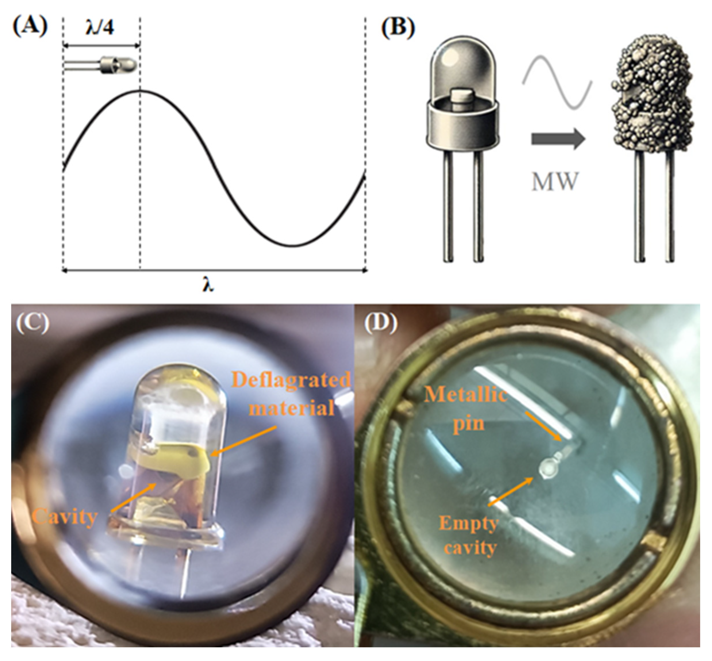
Thermal heating reduces the recovery efficiency within the reflective cavity, as some of the LED chip materials deform, adhere, or become trapped, making the separation and extraction of the chip more difficult. In particular, after conventional heat treatment, the LED chip was only partially recovered (with an efficiency of 45%, determined through mass measurements using a five-digit precision scale), with some material remaining trapped in the cavity (Figure 7). In the case of microwave treatment, the LED chip is 100% recoverable, with a mass remarkably close to the expected value of 0.1 mg per LED, leaving the reflective cavity completely empty (Figure 3D).
(ii)
Conventional heat treatment causes severe oxidation of the metallic pins into iron oxides, which compromises their structural integrity and renders them non-conductive (Figure 8). Silver can be detected in small amounts using XRF but not in the XRD in this case. When heated in air at 800 °C, the iron core oxidizes, forming a thick iron oxide layer. This layer, along with the fact that silver is present in small amounts, can completely obscure the detection of silver by XRD. Thus, direct heating is less favorable as it does not fully recover the LED chip material and causes irreversible damage to the metallic pins, ultimately reducing the recovery efficiency of the LED components.
It is important to note that in this study, the microwave treatment is brief—lasting only one minute—and is followed by a conventional air calcination step. In comparison, direct calcination in air is a lengthier process. As a result, the overall energy efficiency of the two methods is broadly comparable, given the short duration of the microwave phase. However, the microwave irradiation offers a critical advantage beyond energy considerations; it enables the quantitative recovery of the LED chip material from the reflective cavity, which is essential for enhancing the overall effectiveness of the recycling process.

3.4. Scalability, Limitations, and Challenges

The method presented, utilizing a microwave treatment at 700 W followed by acid leaching, has demonstrated an extraction of 96% from a 40 mg LED chip sample, leaving only 1.5 mg of residue. This high efficiency at a laboratory scale suggests a promising foundation for industrial adaptation, particularly given the rapid and effective charring of plastic lenses and simultaneous deflagration of LED chips achieved through microwave processing.
Scaling up the microwave treatment offers several practical advantages for industrial applications. Microwave technology is inherently scalable, as industrial-grade microwave reactors can be designed to handle significantly larger volumes of e-waste while maintaining uniform energy distribution and processing speed. For instance, increasing the capacity from milligrams to kilograms could involve the use of continuous-flow microwave systems, where LED e-waste is processed in batches or fed through a conveyor system, ensuring consistent exposure to the 700 W power level that has proven effective. This scalability preserves the method’s core benefit-rapid processing times—potentially reducing operational costs. Additionally, the precision of microwave energy minimizes material loss and enhances the separation of metals from refractive LED components, supporting a high recovery yield that could translate to industrial-scale efficiency.
From an environmental and economic perspective, the microwave-assisted approach presents notable benefits that merit further exploration in future studies. Environmentally, the method reduces energy consumption compared to conventional high-temperature calcination processes, as the targeted microwave energy achieves charring and deflagration in a fraction of the time, lowering the carbon footprint. Economically, the high extraction rate of valuable metals (96% on average) suggests a cost-effective return on investment, especially given the rising demand for rare and precious metals found in LEDs. While a full comparative analysis with other methods (e.g., pyrometallurgy or hydrometallurgy) requires additional data on energy costs, waste disposal, and throughput rates, the simplicity and speed of this process position it as a competitive alternative. These aspects, though not fully detailed here, underscore the method’s potential and provide a compelling case for subsequent research to quantify its industrial viability.
While the method demonstrates technical promise, it introduces certain limitations and concerns—such as the release of toxic gasses and fumes or the use of hazardous chemicals—that warrant consideration. One limitation of the combined microwave, calcination, and acid leaching approach is the complexity of coordinating these steps at scale. The microwave treatment effectively chars the plastic lens and deflagrates the LED chip, facilitating initial separation, but the subsequent calcination step at 800 °C requires high-energy input and specialized equipment to handle larger volumes, potentially offsetting some of the time and energy savings from the microwave phase. Additionally, the acid leaching process, while effective due to the high insolubility of LED materials, relies on concentrated acids like aqua regia and HCl, which pose handling and disposal challenges in an industrial setting. Scaling this up could increase operational costs and safety risks, as larger quantities of corrosive reagents would need careful management to avoid environmental contamination or worker exposure. Furthermore, the transition between these steps—microwave treatment, calcination, and leaching—may introduce inefficiencies, such as material loss during transfer or inconsistent processing times, which could reduce the overall yield when moving beyond laboratory conditions.
A significant environmental concern arises from the microwave processing itself, particularly the decomposition of the plastic lens, which releases toxic gasses and fumes. During the rapid charring and deflagration at 700 W, the thermal breakdown of plastics and other organic components in the LED chip can produce hazardous emissions, such as volatile organic compounds (VOCs), dioxins, or chlorine-containing gasses, especially given the presence of halogenated materials in some LEDs. In a scaled-up operation, these emissions would require robust gas capture and treatment systems—such as scrubbers or filters—to mitigate air pollution and comply with environmental regulations, adding to the infrastructure costs. While the method’s high recovery rate and speed are advantageous, the release of such fumes could limit its industrial feasibility unless paired with effective mitigation strategies. These challenges, alongside the economic trade-offs of implementing such controls, highlight areas for future research to refine the process and ensure its viability, reinforcing that while the method is promising, its full industrial potential remains to be optimized.

4. Conclusions

In this study, a microwave-assisted recycling method for critical elements present in LED devices is introduced. Microwave irradiation transforms the plastic lens of the LED into a brittle char while simultaneously weakening the adhesion between the semiconducting chip and the metallic pins (Fe, Ni, Ag). This facilitates effortless mechanical separation, significantly reducing the need for labor-intensive or chemically dismantling methods. A key feature of this method is the initiation of a deflagration-like reaction by the microwaves, which rapidly degrades the plastic components and promotes the release and recovery of the embedded LED chip. During microwave processing, the LED chip penetrates the plastic lens and becomes embedded within the charred residue. Subsequent calcination of this residue yields a solid containing all the materials of the LED chip, including critical elements such as Ga, As, In, Y, and Au. A two-step acid treatment, involving aqua regia followed by hot, concentrated HCl, effectively leaches away several of these metals, as shown by complementary analytical techniques. XRD verified the crystalline structure of the isolated materials, while XRF provided detailed insights into elemental composition. The analysis confirmed the successful extraction of key materials, with efficiency reaching 96%, validating the effectiveness of the proposed recycling approach. Beyond its high yield, the method is scalable and industrially viable. The rapid, resonance-driven heating effect of microwaves enables component separation in under a minute—offering a substantial advantage over conventional recycling approaches. Overall, this microwave-assisted method, particularly through deflagration-driven chip release, enhances recycling efficiency and presents a promising solution to the growing challenge of LED e-waste. An outline of the key aspects of the process is provided below:
  • Microwave irradiation converts the plastic LED lens into a brittle char and weakens chip-to-metal pin bonds, enabling easy mechanical separation;
  • A deflagration-like reaction initiated by the microwaves rapidly decomposes the plastic enclosure and enables the release of the LED chip;
  • During microwave treatment, the LED chip becomes embedded in the charred lens residue, aiding its recovery;
  • Calcination of the charred material produces a solid material containing critical elements such as Ga, As, In, Y, and Au;
  • A two-step acid leaching process (aqua regia followed by hot HCl) efficiently extracts valuable metals;
  • The method achieves an extraction efficiency of up to 96%, confirming its high effectiveness;
  • The process is rapid and scalable, completing component separation in approximately one minute—making it well-suited for industrial recycling applications.

Author Contributions

Conceptualization—A.B.B.; data curation—A.B.B., C.P., A.M., N.C., E.P.G., D.P.G., C.E.S. and M.A.K.; formal analysis—A.B.B., C.P., A.M., N.C., E.P.G., D.P.G., C.E.S. and M.A.K.; investigation—A.B.B., C.P., A.M. and N.C., methodology—A.B.B.; supervision—A.B.B., N.C. and M.A.K.; validation—A.B.B., C.P., A.M., N.C., E.P.G., D.P.G., C.E.S. and M.A.K.; writing, original draft—A.B.B., C.P., N.C., E.P.G., C.E.S. and M.A.K.; writing, review and editing—A.B.B., N.C. and E.P.G. All authors have read and agreed to the published version of the manuscript.

Funding

We acknowledge support of this work by the project “Advanced Nanostructured Materials for Sustainable Growth: Green Energy Production/Storage, Energy Saving and Environmental Remediation” (TAEDR-0535821), which is implemented under the action “Flagship actions in interdisciplinary scientific fields with a special focus on the productive fabric” (ID 16618), Greece 2.0-National Recovery and Resilience Fund and funded by the European Union NextGenerationEU. The research project is implemented in the framework of H.F.R.I., “Basic research Financing (Horizontal support of all Sciences)” under the National Recovery and Resilience Plan “Greece 2.0”, funded by the European Union-NextGenerationEU (H.F.R.I. Project Number: 15949). This work made use of the Cornell Center for Materials Research (CCMR) shared instrumentation facility. The authors acknowledge support by the Center for Alkaline-Based Energy Solutions (CABES), part of the Energy Frontier Research Center (EFRC) program supported by the U.S. Department of Energy, under grant DE-SC-0019445.

Data Availability Statement

The datasets generated for this study are available upon reasonable request from the corresponding authors.

Conflicts of Interest

The authors declare no conflicts of interest.

References

  1. Dillon, H.E.; Ross, C.; Dzombak, R. Environmental and energy improvements of LED lamps over time: A comparative life cycle assessment. LEUKOS 2019, 16, 229–237. [Google Scholar] [CrossRef]
  2. Wang, S.; Su, D.; Wu, Y.; Chai, Z. Application of life-cycle assessment to the eco-design of LED lighting products. Euro-Mediterr. J. Environ. Integr. 2020, 5, 41. [Google Scholar] [CrossRef]
  3. Lim, S.-R.; Kang, D.; Ogunseitan, O.A.; Schoenung, J.M. Potential environmental impacts from the metals in incandescent, compact fluorescent lamp (CFL), and light-emitting diode (LED) bulbs. Environ. Sci. Technol. 2013, 47, 1040–1047. [Google Scholar] [CrossRef]
  4. Rahman, S.M.M.; Pompidou, S.; Alix, T.; Laratte, B. A review of LED lamp recycling process from the 10 R strategy perspective. Sustain. Prod. Consum. 2021, 28, 1178–1191. [Google Scholar] [CrossRef]
  5. Wehbie, M.; Semetey, V. Characterization of end-of-life LED lamps: Evaluation of reuse, repair and recycling potential. Waste Manag. 2022, 141, 202–207. [Google Scholar] [CrossRef]
  6. Mandal, S.; Bakaruddin, B.R.B.; Jeon, S.; Lee, Y.; Kim, K.-W. Assessment of the recycling potential of valuable metals by mapping the elemental composition in discarded light-emitting diodes (LEDs). J. Environ. Manag. 2023, 328, 116900. [Google Scholar] [CrossRef]
  7. Illés, I.B.; Kékesi, T. The production of high-purity gallium from waste LEDs by combining sulfuric acid digestion, cation-exchange and electrowinning. J. Environ. Chem. Eng. 2023, 11, 110391. [Google Scholar] [CrossRef]
  8. Ruiz-Mercado, G.J.; Gonzalez, M.A.; Smith, R.L.; Meyer, D.E. A conceptual chemical process for the recycling of Ce, Eu, and Y from LED flat panel displays. Resour. Conserv. Recycl. 2017, 126, 42–49. [Google Scholar] [CrossRef]
  9. Cenci, M.P.; Dal Berto, F.C.; Castillo, B.W.; Veit, H.M. Precious and critical metals from wasted LED lamps: Characterization and evaluation. Environ. Technol. 2022, 43, 1870–1881. [Google Scholar] [CrossRef]
  10. Zhu, P.; Ma, Y.; Wang, Y.; Yang, Y.; Qian, G. Separation and recovery of materials from the waste light emitting diode (LED) modules by solvent method. J. Mater. Cycles Waste Manag. 2020, 22, 1184–1195. [Google Scholar] [CrossRef]
  11. Zhan, L.; Wang, Z.; Zhang, Y.; Xu, Z. Recycling of metals (Ga, In, As and Ag) from waste light-emitting diodes in sub/supercritical ethanol. Resour. Conserv. Recycl. 2020, 155, 104695. [Google Scholar] [CrossRef]
  12. Swain, B.; Mishra, C.; Kang, L.; Park, K.-S.; Lee, C.G.; Hong, H.S. Recycling process for recovery of gallium from GaN an e-waste of LED industry through ball milling, annealing and leaching. Environ. Res. 2015, 138, 401–408. [Google Scholar] [CrossRef] [PubMed]
  13. Chen, W.-S.; Hsu, L.-L.; Wang, L.-P. Recycling the GaN waste from LED industry by pressurized leaching method. Metals 2018, 8, 861. [Google Scholar] [CrossRef]
  14. Annoni, R.; Lange, L.C.; Amaral, M.C.S.; Silva, A.M.; Assunção, M.C.; Franco, M.B.; de Souza, W. Light emitting diode waste: Potential of metals concentration and acid reuse via the integration of leaching and membrane processes. J. Clean. Prod. 2020, 246, 119057. [Google Scholar] [CrossRef]
  15. Rebello, R.Z.; Lima, M.T.W.D.C.; Yamane, L.H.; Siman, R.R. Characterization of end-of-life LED lamps for the recovery of precious metals and rare earth elements. Resour. Conserv. Recycl. 2020, 153, 104557. [Google Scholar] [CrossRef]
  16. Zhan, L.; Xia, F.; Xia, Y.; Xie, B. Recycle gallium and arsenic from GaAs-based e-wastes via pyrolysis-vacuum metallurgy separation: Theory and feasibility. ACS Sustain. Chem. Eng. 2018, 6, 1336–1342. [Google Scholar] [CrossRef]
  17. Li, B.; Tao, R.; Wu, Y.; Zhang, W.; Liu, X.; Wang, W. Study on the pyrolysis characteristics and reaction mechanisms of WLED packaging materials. J. Anal. Appl. Pyrol. 2023, 170, 105935. [Google Scholar] [CrossRef]
  18. Sun, J.; Wang, W.; Liu, Z.; Ma, C. Recycling of waste printed circuit boards by microwave induced pyrolysis and featured mechanical processing. Ind. Eng. Chem. Res. 2011, 50, 11763–11769. [Google Scholar] [CrossRef]
  19. Anis, S.; Lestari, S.E. Production of liquid oil from thermolysis of electrical and electronic wastes (e-waste) under microwave irradiation. J. Phys. Sci. 2018, 29, 53–62. [Google Scholar] [CrossRef]
  20. Anis, S.; Prasetyo, E. Conversion of hand phone case waste into liquid fuels in a microwave reactor. IOP Conf. Ser. Earth Environ. Sci. 2019, 258, 012011. [Google Scholar] [CrossRef]
  21. Huang, Y.-F.; Pan, M.-W.; Lo, S.-L. Hydrometallurgical metal recovery from waste printed circuit boards pretreated by microwave pyrolysis. Resour. Conserv. Recycl. 2020, 163, 105090. [Google Scholar] [CrossRef]
  22. Anis, S.; Qudus, N.; Kusumastuti, A. Treatment of electrical and electronic waste to reduce environmental issue. J. Adv. Res. Fluid Mech. Therm. Sci. 2020, 72, 148–156. [Google Scholar] [CrossRef]
  23. Risco, Á.; Sucunza, D.; González-Egido, S. Chemical recovery of waste electrical and electronic equipment by microwave-assisted pyrolysis: A review. J. Anal. Appl. Pyrol. 2021, 159, 105323. [Google Scholar] [CrossRef]
  24. Andooz, A.; Eqbalpour, M.; Kowsari, E.; Ramakrishna, S.; Cheshmeh, Z.A. A comprehensive review on pyrolysis of e-waste and its sustainability. J. Clean. Prod. 2022, 333, 130191. [Google Scholar] [CrossRef]
  25. Horikoshi, S.; Hachisuga, N.; Serpone, N. Recycling of e-waste power cables using microwave-induced pyrolysis-process characteristics and facile recovery of copper metal. RSC Adv. 2024, 14, 29955–29964. [Google Scholar] [CrossRef]
  26. Bourlinos, A.B.; Spyrou, K.; Moschovas, D.; Avgeropoulos, A.; Salmas, C.; Karakassides, M.A. Fast microwave carbonization of aluminum-coated plastic wastes and perspectives: The examples of CDs and snack bags. Next Mater. 2025, 6, 100333. [Google Scholar] [CrossRef]
  27. Chalmpes, N.; Spyrou, K.; Vasilopoulos, K.C.; Bourlinos, A.B.; Moschovas, D.; Avgeropoulos, A.; Gioti, C.; Karakassides, M.A.; Gournis, D. Hypergolics in Carbon Nanomaterials Synthesis: New Paradigms and Perspectives. Molecules 2020, 25, 2207. [Google Scholar] [CrossRef]
  28. Bourlinos, A.B.; Chalmpes, N.; Giannelis, E.P.; Gournis, D.P.; Moschovas, D.; Avgeropoulos, A.; Salmas, C.; Karakassides, M.A. Total recycling of copper cable scrap and production of carbon using fast microwave technology. Eng 2025, 6, 74. [Google Scholar] [CrossRef]
  29. Chalmpes, N.; Tantis, I.; Alsmaeil, A.W.; Bourlinos, A.B.; Giannelis, E.P. Design, synthesis, and evaluation of noble metal nanoparticles and in situ-decorated carbon-supported nanoparticle electrocatalysts using hypergolic reactions. Chem. Mater. 2025, 36, 10616–10625. [Google Scholar] [CrossRef]
  30. Delgado, M.R.; Areán, C.O. Surface chemistry and pore structure of β-Ga2O3. Mater. Lett. 2003, 57, 2292–2297. [Google Scholar] [CrossRef]
  31. Shi, F.; Qiao, H. Influence of hydrothermal reaction time on crystal qualities and photoluminescence properties of β-Ga2O3 nanorods. J. Mater. Sci. Mater. Electron. 2020, 31, 20223–20231. [Google Scholar] [CrossRef]
  32. Meitei, S.R.; Devi, L.S.; Singh, N.K. Nanocrystalline β-Ga2O3 thin film prepared by electron beam evaporation for enhanced photodetection. J. Phys. D Appl. Phys. 2023, 56, 395104. [Google Scholar] [CrossRef]
  33. Bioud, Y.A.; Boucherif, A.; Belarouci, A.; Paradis, E.; Drouin, D.; Arès, R. Chemical composition of nanoporous layer formed by electrochemical etching of p-type GaAs. Nanoscale Res. Lett. 2016, 11, 446. [Google Scholar] [CrossRef] [PubMed]
  34. Verma, Y.; Rana, S.V.S. Hepatotoxic manifestations of arsenic trioxide loaded poly (lactide-coglycolide) nanoparticles in wistar rat. J. Anesth. Pain Med. 2024, 9, 1–9. [Google Scholar]
  35. El-Faramawy, N.; Gad, A.; Alazab, H.A.; Farouk, S. Thermoluminescence assessment of quartz veins emplaced in Talc-Schist Metamorphic Rocks, Egypt. J. Mater. Res. 2022, 37, 3784–3791. [Google Scholar] [CrossRef]
  36. Chen, W.-T.; Tsai, L.-C.; Tsai, F.-C.; Shu, C.-M. Recovery of gallium and arsenic from gallium arsenide waste in the electronics industry. Clean-Soil Air Water 2012, 40, 531–537. [Google Scholar] [CrossRef]
  37. de Oliveira, R.P.; Benvenuti, J.; Espinosa, D.C.R. A review of the current progress in recycling technologies for gallium and rare earth elements from light-emitting diodes. Renew. Sustain. Energy Rev. 2021, 145, 111090. [Google Scholar] [CrossRef]
  38. Vinhal, J.T.; de Oliveira, R.P.; Coleti, J.L.; Espinosa, D.C.R. Characterization of end-of-life LEDs: Mapping critical, valuable and hazardous elements in different devices. Waste Manag. 2022, 151, 113–122. [Google Scholar] [CrossRef]
  39. Balinski, A.; Recksiek, V.; Stoll, M.; Christesen, C.; Stelter, M. Liberation and separation of valuable components from LED modules: Presentation of two innovative approaches. Recycling 2022, 7, 26. [Google Scholar] [CrossRef]
  40. Illés, I.B.; Kékesi, T. A comprehensive aqueous processing of waste LED light bulbs to recover valuable metals and compounds. Sustain. Mater. Technol. 2023, 35, e00572. [Google Scholar] [CrossRef]
  41. Lavalley, J.C.; Daturi, M.; Montouillout, V.; Clet, G.; Areán, C.O.; Delgado, M.R.; Sahibed-dine, A. Unexpected similarities between the surface chemistry of cubic and hexagonal gallia polymorphs. Phys. Chem. Chem. Phys. 2003, 5, 1301–1305. [Google Scholar] [CrossRef]
  42. Chiang, J.-L.; Yadlapalli, B.K.; Chen, M.-I.; Wuu, D.-S. A review on gallium oxide materials from solution processes. Nanomaterials 2022, 12, 3601. [Google Scholar] [CrossRef]
  43. Sharma, A.; Varshney, M.; Saraswat, H.; Chaudhary, S.; Parkash, J.; Shin, H.-J.; Chae, K.-H.; Won, S.-O. Nano-structured phases of gallium oxide (GaOOH, α-Ga2O3, β-Ga2O3, γ-Ga2O3, δ-Ga2O3, and ε-Ga2O3): Fabrication, structural, and electronic structure investigations. Int. Nano Lett. 2020, 10, 71–79. [Google Scholar] [CrossRef]
  44. Zhang, Y.; Yan, J.; Li, Q.; Qu, C.; Zhang, L.; Xie, W. Optical and structural properties of Cu-doped β-Ga2O3 films. Mater. Sci. Eng. B 2011, 176, 846–849. [Google Scholar] [CrossRef]
Figure 1. Schematic of the primary components of an LED.
Chemengineering 09 00047 g001
Figure 2. (Left) Microwave irradiation of LEDs (5 mm round T-1¾) placed in a silica ceramic crucible (outer diameter: 5.8 cm) causes ignition, leading to the formation of residue consisting of metallic pins and brittle charred plastic lenses (AC). Manual separation using hand abrading and attraction by a magnet easily extracts the metallic pins (D), referred to as PNLED (length: 2.5–3.0 cm). Apart from being magnetic, the metallic pins also exhibit a conductive behavior as tested with a multimeter (E). The brittle, charred plastic lenses encasing the LED chip material can be easily detached (2.5 g from 400 LEDs) (F) and can be further processed through calcination in air to obtain SMLED (40 mg from 400 LEDs) (G). (Right) The corresponding flowchart including the two-stage acid leaching process.
Chemengineering 09 00047 g002
Figure 3. The size of the LED corresponds to one fourth of the microwave’s standing wave wavelength at maximum intensity (A). This results in a strong interaction with microwaves, leading to the formation of a brittle charred plastic lens loosely attached to the metallic pins (B). The brittle, charred plastic lens encases the yellow semiconducting LED chip material, which deflagrates from the reflective cavity towards the plastic lens during the initial stages of microwave treatment (C). As a result, the cavity within the metallic pins is left empty, devoid of any semiconducting material (D). Photos (C,D) were taken using a magnifying loupe.
Chemengineering 09 00047 g003
Figure 4. (Left) XRD pattern of PNLED. (Right) XRF spectrum of PNLED.
Chemengineering 09 00047 g004
Figure 5. (Left) XRD pattern of SMLED. Reflections of iron (✧) and tin (◆) oxide are also indicated. (Right) XRF spectrum of SMLED. The marked energy regions are detailed in the inset figures. Peak notation corresponds to the following: (a) Fe Kα, (b) Fe Kβ, (c) Cu Kα, (d) Ga Kα, (e) Au Lα, (f) Ga Kβ, (g) As Kα/Pb Lα, (h) Au Lβ/As Kβ, (i) Pb Lβ2, (j) Au Lγ, (k) Sr Kα, (l) Y Kα, (m) Sr Kβ/Zr Kα, (n) Y Kβ, (o) Ag Kα, (p) In Kα, (q) Sn Kα/Ag Kβ, (r) Sn Kβ1, (s) Sn Kβ2, (t) Ba Kα, (u) La Kα, (v) Ce Kα, (w) Gd Kα2, (x) Gd Kα1. Some of the detected XRF peaks are not discernible in this illustration.
Chemengineering 09 00047 g005
Figure 6. (Left) XRD pattern of SMLEDH. The 111 and 400 reflections are attributed to residual β-Ga2O3. Reflections of iron oxide (✧) are also indicated. (Right) XRF spectrum of SMLEDH. The marked energy regions are detailed in the inset figures. Peak notation is explained in Figure 5.
Chemengineering 09 00047 g006
Figure 7. Unlike microwave treatment, direct calcination of LED fails to sufficiently recover the chip from the reflective cavity. The photo was taken using a magnifying loupe.
Chemengineering 09 00047 g007
Figure 8. XRD pattern of the metallic pins following the direct calcination of LEDs in air at 800 °C. The inset highlights a heavily oxidized blackish pin, in contrast to the silvery, lustrous pin achieved through microwave treatment, as well as its lack of conductivity.
Chemengineering 09 00047 g008
Table 1. Elemental concentrations determined by XRF spectrometry. Leaching efficiency values following acid treatment are also listed.
ElementElemental Concentrations (% w/w) 1Leaching Efficiencies (%) 2
PNLEDSMLEDSMLEDHSMLEDHHSMLEDHSMLEDHH
Fe61.026.736.8 7100
Ni37.0
Cu 10.80.3 98100
Ga 2.53.46.0991
As 1.3327 * 98100
Sr 406 *92 *704 *8593
Y 0.240.32 10100
Zr 202 *161 *0.14681
Ru 269 *138 * 65100
Rh 39 * 100
Ag1.01.50.6614 *7396
In 570 *142 * 83100
Sn 2.01.30.55999
Ba 185 *40 * 85100
La 140 *158 *994 *2473
Ce 224 *265 * 20100
Gd 344 *567 * 0100
Au1.01.5 100100
Pb 426 *403 *443 *3696
SMLEDH (27 mg) refers to the first acid treatment, while SMLEDHH (1.5 mg) refers to the second acid treatment. 1 Values denoted with * are given in ppm. 2 All values refer to metal leaching from SMLED (40 mg).
Disclaimer/Publisher’s Note: The statements, opinions and data contained in all publications are solely those of the individual author(s) and contributor(s) and not of MDPI and/or the editor(s). MDPI and/or the editor(s) disclaim responsibility for any injury to people or property resulting from any ideas, methods, instructions or products referred to in the content.

