Abstract
Tantalum nitride (TaN) is a typical transition metal nitride characterized by a wide range of tunable resistivity. Low-resistance TaN even exhibits a resistivity similar to that of metals. Given that electrical resistance influences secondary electron emission (SEE) behavior, this study investigates the relationship between TaN film resistivity and SEE characteristics. Five TaN films were deposited by varying the N2 gas flow rate during sputtering. Morphological analyses revealed that the film thicknesses ranged from approximately 197 to 281 nm. X-ray photoelectron spectroscopy (XPS) results indicated that the Ta:N atomic ratio of the films ranged from approximately 0.53 to 0.87. Furthermore, XPS detected non-adsorbed oxygen on the surfaces of the TaN films, and more detailed XPS analysis revealed the formation of TaON compounds on the surfaces due to oxygen exposure. X-ray diffraction patterns confirmed that the TaN films contained two crystal phases: Ta2N (002) and TaN (200). Sheet resistivity tests showed that the resistivity of the TaN films ranged from 5.67 × 10⁻³ to 2.43 Ω·cm. Furthermore, the lower the Ta:N atomic ratio was, the lower the electrical resistivity of the films became. SEE coefficient (SEEC) showed a clear positive correlation with the films’ electrical resistivity. Specifically, films with lower resistivity exhibited reduced SEEC values. When the N2 gas flow rate was 16 sccm (N2:Ar = 16:0), the film exhibited the smallest SEEC (maximum ~1.88); when the N2 flow rate was 0 sccm (N2:Ar = 0:16), the film showed the largest SEEC (maximum ~2.25). This research provides valuable references for expanding the application of TaN films in engineering scenarios involving electrical resistivity adjustment and SEE applications.
1. Introduction
Tantalum nitride (TaN) is a versatile, high-performance ceramic material that plays a critical role in key technologies across diverse fields, such as integrated circuit manufacturing and aerospace [1,2,3,4]. Published research indicates that TaN exhibits excellent physical properties, including thermal stability, chemical inertness, excellent diffusion barrier properties, tunable resistivity, and high stiffness, making it ideally suited for film applications where reliability is critical under extreme conditions [3,4,5]. Additionally, TaN finds applications in micro-electromechanics and energy harvesting [5,6,7]. In the field of semiconductor manufacturing, TaN films serve as a diffusion barrier in copper interconnect technology to prevent the rapid diffusion of copper atoms into the surrounding silicon, which is a critical capability for nanoscale features in advanced chips [8,9,10]. In addition, TaN is a key material for metal gates in transistors, acting as a stable electrode and functional layer for work function tuning in MOSFETs [10,11,12]. In addition, by combining its excellent stability with the metallic/semi-metallic conductivity it exhibits in certain phases, TaN is considered an ideal candidate for electrodes in a variety of miniature sensors used in harsh environments [13,14]. In coating engineering, TaN films excel as protective coatings against high temperatures, thermal cycling, radiation exposure, friction, and oxidizing environments [15,16]. In addition, TaN coatings can be used as functional layers on electronic components in satellites and spacecraft to protect them from the damaging effects of cosmic rays and solar radiation, with the chemical inertness and oxidation resistance of TaN ensuring long-term performance stability in challenging environments [16,17,18].
Various transition metal nitrides have physical and chemical properties similar to those of TaN [3], among which titanium nitride (TiN) is one with physical and chemical properties extremely similar to TaN’s, including adjustable metal-like conductivity [19], excellent wear and high-temperature resistance [20,21,22], and superior chemical stability (i.e., low reactivity with other substances) [22]. In addition, the low secondary electron emission (SEE) coefficient (SEEC) of TiN material renders it widely applicable in scenarios where secondary electron multiplying discharges are suppressed [23,24,25,26]. Typical scenarios where TiN is applied to reduce SEEC include suppressing electron cloud formation in particle accelerators [23], and mitigating multipactor effects in space-borne microwave systems [25,26]. Given the similar physical properties of TaN and TiN, it is scientifically meaningful to investigate whether TaN can serve as a novel functional material for SEEC modulation in electron emission-related applications. From previous studies, it is known that the SEEC of films partly depends on their resistance characteristics [27]. Although there has been very little research on the electron emission behavior of TaN films, there have been reports on the control of electrical resistivity in TaN films [28,29,30]. For example, in 2004, Lal et al. investigated the resistive properties of TaN thin films deposited by ion beam-assisted deposition, and found that the non-metallic behavior of TaN arises from nitrogen-induced carrier localization effects. They also tuned the resistivity of TaN films from 789 μΩ·cm to 2882 μΩ·cm by controlling the nitrogen content [28]. In 2018, by employing the technology of 30 keV nitrogen ion implantation, Ramezani et al. achieved a controllable increase in the resistivity of TaN films from 182.7 mΩ·cm to 272.6 mΩ·cm, uncovering the synergistic regulatory mechanism of the nitrogen implantation dose on TaN phase transformation, surface morphology, and electrical properties [29]. In 2021, Jiang et al. investigated the electrical resistance control of TaN films under oxygen incorporation, concluding that oxygen doping enabled precise tuning of the resistivity of cubic TaN thin films over seven orders of magnitude (i.e., from 5.3 × 10⁻⁴ S/m to 4.1 × 10³ S/m) [30]. The above studies showed that TaN exhibits excellent resistivity tunability. Although few studies have focused on the electron emission of TaN, it is hypothesized that TaN may exhibit unique SEEC behavior, similar to TiN.
In this work, by controlling the gas flow rate of N2 during sputtering, we investigated the composition, electrical resistivity, and SEEC performance for TaN films, to reveal the tunability of the electrical resistivity of TaN films, and see whether it can be used in certain applications involving electron emission. We conducted a systematic study on the influence of the gas flow rate on the composition of TaN films. Additionally, we presented the experimental relationship between the elemental composition and the electrical resistivity of TaN films. Also, experiments were implemented to explore the influence of film electrical resistivity on SEEC. To theoretically explain the experimental results, the potential physical mechanisms by which free-electron concentration affects the SEEC process was discussed. This research provides valuable insights for expanding the application of TaN materials in the field of vacuum electron emission.
2. Results and Discussion
2.1. Surface and Fracture Surface Characterization of TaN Films
Here, five TaN film samples, denoted as #1–#5, were fabricated using reactive magnetron sputtering. During the sputtering process, to investigate the effect of the gas ratio on film formation and the films’ physical properties, the N2:Ar gas flow ratios for #1–#5 TaN films were set to 0:16, 4:16, 8:16, 12:16, and 16:16, respectively. Figure 1 presents the surface morphologies and fracture cross-sections of the TaN films, as characterized by scanning electron microscopy (SEM), at the same magnification. Figure 1a–d are the SEM micrographs of the top view for the #1, #2, #3, #5 TaN films, while Figure 1e–h are the corresponding fracture surface images. By comparing the surface morphologies of the TaN films in Figure 1, it is evident that the N2:Ar gas flow ratio during the sputtering process has some effect on the films’ surface morphology. Specifically, as shown in Figure 1a, when no N2 was introduced during deposition (i.e., N2:Ar = 0:16), the TaN film surface exhibits numerous raised, irregular nanostructures; the grain size is approximately tens of nanometers, with distinct grain boundaries. When the gas flow rate increases (to N2:Ar = 4:16), as shown in Figure 1b, the grain size decreases significantly. Detailed inspection of Figure 1b reveals that the grain size is about tens of nanometers, and the grain boundaries are no longer obvious. As for the cases where the N2:Ar gas flow rate ≥8:16, no distinct grains or grain boundaries are visible on the surface in Figure 1c,d, except for tiny contamination particles. The above results indicate that the grain size of the prepared TaN films is relatively large and crystal grain boundaries are obvious when the N2 gas flow rate is low under the experimental conditions. Conversely, when the N2 flow rate is increased, the grains of TaN films become smaller.
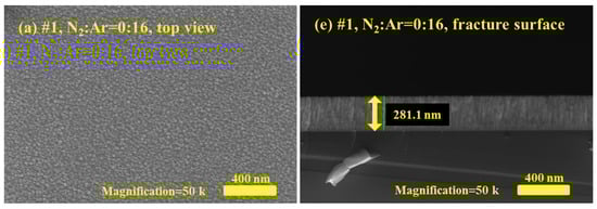
Figure 1.
Surface morphology and fracture surface micrographs of #1, #2, #3, and #5 TaN film samples characterized by SEM; (a–d) are the top view of the SEM micrographs for TaN film samples when N2:Ar = 0:16, 4:16, 8:16, and 16:16, (e–h) are the corresponding fracture surface micrographs.
The thickness information of the TaN film samples can be obtained from the fracture surface images in Figure 1e–h, where the thickness is marked with a yellow line segment. Using the software embedded in the SEM system, the approximate thicknesses of samples #1–#5 were determined to be 281 nm, 251 nm, 239 nm, 213 nm, and 197 nm, respectively. Here, it is found that the film thicknesses of the film samples decrease progressively as the N2 gas flow rate rises. This result suggests that increasing the N2 gas flow rate reduces the sputtering rate. In fact, during the experiment, N2 was the main reaction gas, while Ar served as the primary gas for ionization and collisional sputtering. Consequently, a lower Ar concentration reduced the sputtering rate, leading to reduced film thickness for the same deposition time.
2.2. Elemental Content Characterization of TaN Films
The surface elemental composition of the prepared TaN films was further analyzed using energy-dispersive X-ray spectroscopy (EDS)—an accessory to the SEM system. Figure 2 presents the EDS results for the TaN films: Figure 2a, EDS spectra of samples #1–#5; Figure 2b, SEM micrograph of the EDS analysis area for sample #3 (the entire area was scanned); and Figure 2c–e, EDS elemental mappings of Ta, N, and O, respectively, for the area in Figure 2b. Table 1 presents the elemental compositions in the different TaN films obtained from EDS analysis. To obtain more accurate results for the elemental distribution, EDS scans were performed on three randomly selected areas, and the average elemental contents are presented in Table 1 (with a maximum error margin of ±9%). Here, Figure 2a indicates that the peak intensity of each element in the EDS spectrum of sample #1 is significantly higher than those in the spectra of the other samples, owing to two factors: Sample #1 is thicker than the other samples, and the EDS detection depth exceeds the film thickness. Comparison of the elemental distributions in Figure 2c–e reveals that the elemental densities of Ta and N inside sample #3 are significantly higher than those of O. This indicates that the O content is very low within the EDS detection depth, which is consistent with the results in Table 1. In fact, no oxygen-containing substances were involved in the deposition process, suggesting that the oxygen likely originates from atmospheric exposure prior to SEM/EDS testing, leading to the formation of an ultrathin contamination layer of a few nanometers on the sample surface. In addition, the EDS results show that Si is also detected, originating from the substrate, since the EDS detection depth is typically in the submicron-to-micron range, which exceeds the thickness of the TaN films.
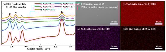
Figure 2.
(a) EDS spectra of TaN films #1–#5; (b) the EDS testing area of sample #3 characterized by SEM, the whole area in this image was scanned by EDS; (c–e) the elemental distribution of Ta, N, and O inside sample #3, characterized by EDS.

Table 1.
Experimentally determined atomic ratios of TaN films by EDS, excluding the substrate Si (the average value obtained from three EDS tests, with an error of no more than ±6%).
After excluding Si (from the substrate) from the EDS data, the relative contents of Ta, N, C, and O were derived, as shown in Table 1. The statistical EDS results in Table 1 indicate that the deposited TaN films are primarily composed of four elements: Ta, N, C, and O. The proportions of these elements vary significantly with the N2 content in the sputtering gas mixture. The presence of C and O suggests gas adsorption and organic contamination on the film surface prior to their entry into the analysis chamber. After accounting for C and O contamination, the Ta:N atomic ratios (derived from the third and fourth columns in Table 1) show that as the N2 flow rate increases during deposition, the N content in the films increases significantly, while the Ta content decreases. The Ta:N atomic ratio data are presented in the last column of Table 1, further confirming the variation in the Ta:N ratio within the films. Specifically, the Ta:N ratio is 0.739 when the N2 flow rate is 0 sccm, decreasing to 0.254 when the N2 flow rate reaches 16 sccm. These results confirm that the prepared films meet the experimental design expectations.
2.3. Accurate Composition Characterization of TaN Films
X-ray photoelectron spectroscopy (XPS) is another precise method used for surface elemental analysis, with detection depths typically in the range of a few to tens of nanometers. XPS is therefore well suited for the quantitative analysis of the most superficial elements of the outermost layers of the prepared TaN films. Figure 3 shows the XPS results of samples #1–#5. Figure 3a shows the binding energy positions corresponding to the various elemental characteristic peaks, as well as the intensities of these peaks. In the XPS spectra in Figure 3, the characteristic peaks at binding energies of about 396 eV, 25 eV, 283 eV, and 530 eV correspond to N 1s, Ta 4f, C 1s, and O 1s, respectively. Additional characteristic peaks of Ta (e.g., Ta 4d and Ta 4p) are also observed. In Figure 3a, the presence of C 1s and O 1s peaks indicates the adsorption of organic contamination on the film surfaces. Analysis of the peak intensities in Figure 3a reveals that as the N2 flow rate increases, the relative contents of N and Ta in the films increase significantly, while the O content decreases notably. Meanwhile, the C 1s peak intensity does not change much, indicating that the degree of organic contamination on the film surface is comparable across the five samples. A fine spectral analysis of high-resolution XPS spectra of N 1s (Figure 3b), Ta 4f (Figure 3c), O 1s (Figure 3d), and C 1s (Figure 3e) for sample #3 reveals that O is not only present as oxy-organic (alkanes, hydrocarbons, etc.) contamination and adsorbed impurity gases, but also reacts with Ta to form Ta2O5. The double peak of O 1s in Figure 3d indicates that a portion of the O is present as TaON (tantalum oxynitride) on the film surface, with the remainder originating from surface contamination. The results in Figure 3b–d indicate that the TaN films have a surface layer composed of TaON in their outermost regions. However, the O element detected on the TaN sample surface likely originates from multiple sources. Here, potential oxygen originates from three main sources, including (1) residual oxygen gas in high-purity gases; (2) residual adsorbed inorganic oxygen-containing compounds (H2O vapor, CO2, CO, etc.) on the vacuum chamber inner surfaces; and (3) organic contamination (oxy-organics, including alkanes, hydrocarbons, etc.) during atmospheric exposure between film deposition and XPS analysis.
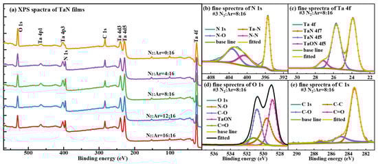
Figure 3.
(a) XPS spectra of samples #1–#5; (b–e) N 1s, Ta 4f, O 1s, and C 1s fine spectra of sample #3 when N2:Ar = 8:16.
Table 2 presents the surface elemental compositions (atomic percentages) of the five TaN films, as determined by XPS. Comparison of the XPS results in Table 2 with the EDS data in Table 1 reveals that the O content measured by XPS is significantly higher. Since the detection depth of XPS is in tens of nanometers from the surface, the oxidation of TaN to form a thin TaON layer confined to the film’s outermost surface is detected more easily. In addition, the data in Table 2 show that the C content in the five TaN films is comparable, indicating that the degree of organic contamination on the sample surfaces is similar across all samples. In addition, for samples #1–#5, the results in Table 2 demonstrate that the Ta:N atomic ratio gradually decreases as the N2 flow rate increases, confirming that adjusting the N2 flow rate is an effective way of tuning the film composition.
Table 2.
Surface elemental composition of TaN films obtained by XPS.
Considering that both the EDS and XPS results showed severe C and O contamination on the sample surface, ion cleaning was performed on sample #3, and the surface elemental composition was re-monitored. The results are shown in Figure 4. The sample surface was irradiated with a 500 eV Ar+ beam for 1 and 3 min, respectively, and in situ XPS spectra were acquired after each cleaning step. The results in Figure 4 show that the ion cleaning process effectively cleaned the sample surface and removed organic contaminants and ultrathin oxide layers. After 3 min of ion cleaning, the C and O contamination on the sample surface was almost completely removed. Based on the sputtering rate of the Ar+ source, the total thickness of the C- and O-containing contamination layer on the sample surface was approximately 3 nanometers.
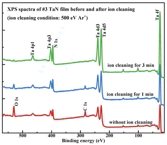
Figure 4.
XPS spectra of TaN #3 sample before and after ion cleaning treatment; ion cleaning conditions: 500 eV Ar+ irradiation, for 1 min and 3 min.
2.4. Crystal Structure Characterization of the TaN Films
To further study the crystalline properties of the TaN films, the crystal structures of the five films were characterized using X-ray diffraction (XRD). Since the samples had been prepared some time ago (approximately two months before XRD), all samples were annealed at 600 °C for 2 h in an Ar atmosphere prior to XRD analysis to ensure the desorption of surface organic contaminants. Figure 5 shows the XRD patterns of the five samples after annealing. Comparison with standard XRD databases confirms that the prepared TaN films primarily consist of two crystalline phases: Ta2N (002) and TaN (200), with 2θ values of 38.1° and 41.7°, respectively. Furthermore, the crystalline orientation of the TaN films varies with deposition conditions. To be specific, TaN films prepared under low N2 gas ratios exhibit a stronger TaN (200) diffraction peak, while those prepared under high N2 gas ratios exhibit a stronger Ta2N (002) peak. In fact, the prepared TaN films may still contain minor secondary phases, possibly including TaON, but due to their low content, the signal is very weak and is masked by background noise. This result also confirms that the TaON content is negligible within the detection depth of XRD (approximately several micrometers). Combined with the XPS results in Figure 3, it can be reasonably inferred that the TaON component on the surface of the prepared TaN films only exists within a few nanometers of the film surface.
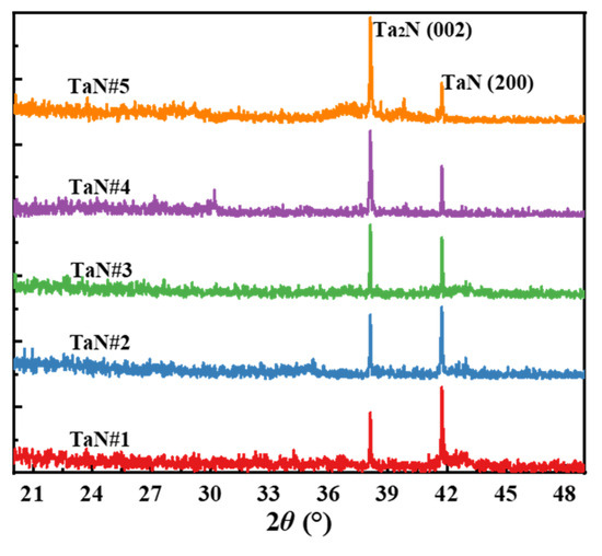
Figure 5.
XRD patterns of five TaN films after annealing treatment.
2.5. Characterization of Electrical Resistivity Property for the TaN Films
In addition to the microanalysis of the TaN film samples, the electrical resistivity of the films was characterized using the four-probe method. It should be noted that since the Si substrate is a semiconductor material, the accuracy of the test results may be affected when the four-probe technique is used for sheet resistance testing. Here, to eliminate the effect of the substrate on the test results, glass substrates were used instead to eliminate substrate-induced errors in sheet resistance measurements. In addition, to minimize random errors and improve data reliability, sheet resistance was measured at three random locations on each film, and the average value was used. It should be noted that the resistivity test is conducted across the thickness of the film layer. Therefore, the surface contamination layer is only about 3 nm thick, which has a negligible effect on the four-probe test current. As a result, the influence of the surface contamination layer on the resistivity test results can be disregarded. The values of the electrical properties of the five TaN films are presented in Table 3. The sheet resistance data presented in Table 3 are the average values of three sets of measurements, with a relative error of less than ±40%. It should be noted that, given the significant differences in film resistivity (typically across an order of magnitude), a relative error of less than ±40% in the measured data is acceptable. Furthermore, the thicknesses of the films in Table 3 were obtained from the SEM fracture surface analysis in Figure 1. Finally, the electrical resistivity, ρ, of the TaN films can be calculated by the following equation:
where R is the sheet resistance and t is the film thickness. The calculated film electrical resistivity is presented in the last column of Table 3.
Table 3.
Sheet resistance and electrical resistivity of five TaN films.
From the data in Table 3, it is evident that the electrical resistivity tends to decrease as the N2:Ar gas flow ratio increases during sputtering. However, it is clear that the gas flow rate is not a direct factor affecting the film electrical resistivity. In fact, it is evident from Table 1 and Table 2 that the gas flow rate directly affects the elemental ratio of Ta and N during film formation, and it is known that the Ta:N ratio affects the film electrical resistivity, as reported in Refs. [29,30]. To illustrate this relationship, Figure 6 shows how electrical resistivity depends on the film’s elemental composition. Figure 6a,b show the effect of the N2:Ar gas flow rate and XPS-measured Ta:N atomic ratio on the electrical resistivity of the TaN films, respectively. From Figure 6b, it is clear that the elemental composition in the TaN films has a significant effect on film electrical resistivity, with resistivity varying by up to three orders of magnitude over the range of process parameters used in this work. To be specific, Figure 6b indicates that a lower Ta:N atomic ratio corresponds to lower electrical resistivity, and the lowest electrical resistivity of 2.75 × 10⁻³ Ω·cm was achieved at Ta:N = 0.52 (XPS results) when N2:Ar = 12:16. In addition, the film’s crystal structure also affects the films’ resistivity. The results of previous studies [31,32] have shown that the resistivity of Ta2N (approximately 200 μΩ·cm) is significantly lower than that of TaN (over 1000 μΩ·cm). From the XRD results in Figure 5, it is observed that the intensity of the Ta2N (002) diffraction peak (indicating increased Ta2N crystallinity) gradually increases for samples #1 to #5, which is consistent with the relationship between crystal structure and resistivity reported in Refs. [31,32].
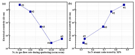
Figure 6.
Variation tendency of electrical resistivity for TaN films: (a) electrical resistivity versus the N2:Ar gas flow ratio; (b) electrical resistivity versus the Ta:N atomic ratio measured by XPS.
2.6. SEE Characterization of TaN Films
SEE is an important physical phenomenon in a vacuum environment. The SEE phenomenon involves a variety of vacuum scenarios, including electron multipliers [33], space-borne electrostatic discharge [34], secondary electron multiplicative discharge [35,36], and surface charging/discharging of space-borne dielectrics [37]. SEEC is a physical parameter that quantifies the number of secondary electrons induced by collisions between electrons and solid surfaces. Specifically, SEEC is defined as the ratio of the number of secondary electrons emitted from a solid surface to the number of incident primary electrons. Considering that the TaN films studied in this work have similar electrical resistivity tunability as TiN, as reported in Reference [30], it is hypothesized that the resistance-tunable properties of TaN films may have applications in SEEC modulation studies similar to TiN [23,24,25,26]. In addition, TaN films are also expected to be promising for applications requiring low SEEC due to their low electrical resistivity, similar to TiN films [27,30,38]. These considerations highlight the significance of investigating the SEEC of TaN films, and the SEEC behavior of the prepared TaN films was thus investigated.
The measured SEEC curves of the TaN films are shown in Figure 7a. During SEEC testing, three measurements were performed on each sample to minimize errors, and the data closest to the average was used for the plots in this study. The relative uncertainty of the SEEC measurements was within ±10%. Figure 7 shows that the SEEC of each film first increases and then decreases with increasing primary electron energy. This trend arises from two factors: the varying ability of primary electrons (with different energies) to excite internal secondary electrons along their paths, as well as the varying probability of these internal secondary electrons escaping to the surface as emitted secondary electrons. Specifically, low-energy primary electrons (tens of eV) excite very few internal secondary electrons, resulting in a low SEEC. As the primary electron energy increases, the primary electron penetrates deeper into the solid, losing energy along the way, exciting more internal secondary electrons and thus increasing the SEEC. However, when the energy of the primary electrons continues to rise, although they can excite more internal secondary electrons along their motion path, these internal secondary electrons are further away from the surface. This increased distance makes it difficult for these internal secondary electrons to reach the surface and escape, thus reducing the electron emission probability. Hence, the SEEC’s first increasing then decreasing trend with incident energy is a result of the combined effects of internal electron excitation and escape probability.
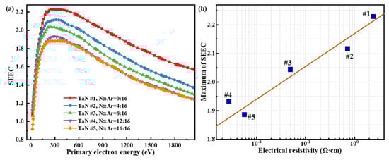
Figure 7.
(a) SEEC of TaN films versus the primary electron energy; (b) maximum SEEC versus the film electrical resistivity.
Figure 7a shows that the SEEC of the TaN film samples gradually decreases and eventually stabilizes as the N2:Ar gas flow ratio increases. Specifically, the maximum SEEC of the TaN films is ~2.23 when the N2 gas flow rate is 0, and the maximum SEEC of the prepared TaN film sample decreases to ~1.89 when the N2 gas flow rate reaches 16 sccm. In fact, the SEEC reduction can be directly attributed to declining film resistivity, as lower resistivity enhances electron scattering. Increased N2 flow rates promoted nitrogen incorporation (evidenced by the XPS in Table 2), which reduced the Ta:N atomic ratio and consequently decreased electrical resistivity. From the perspective of the physical process of electron–matter interaction, the phenomenon of the SEEC decrease induced by electrical resistivity variation can be explained as follows. Since the motion of excited internal secondary electrons is sharply affected by scattering with internal free electrons, the scattering probability determines the likelihood of internal secondary electrons being emitted. Specifically, the greater the scattering probability of internal secondary electrons, the more severe their energy loss, and the lower their emission probability, macroscopically resulting in a lower SEEC. Therefore, the concentration of free electrons is an important factor in determining the electrical resistivity of the TaN films, i.e., a higher free-electron concentration corresponds to lower resistivity, and vice versa. Therefore, sample #1, with relatively higher electrical resistivity, exhibits a higher SEEC, while samples #4 and #5, with relatively lower electrical resistivity, exhibit lower SEEC values. The results in Figure 7b show an approximately linear increase in maximum SEEC as the film resistivity increases exponentially, indicating a potential mathematical relationship between resistivity and SEEC for TaN films. In Figure 7b, an approximate logarithmic fit is applied to describe the dependence of the maximum SEEC on film resistivity, which allows for the approximate estimation of the maximum SEEC of TaN films under other resistivity conditions. The expression of this logarithmic fitting curve is as follows:
3. Methods
3.1. TaN Film Preparation
The TaN films were deposited using direct current magnetron sputtering (self-made equipment). N-type silicon wafers and glass slides were used as substrates. Prior to deposition, the substrates were cleaned sequentially with acetone, ethanol, and ultrapure water to remove surface contaminants. The sputtering source was a 99.99%-pure TaN target with a diameter of 50.8 mm and a thickness of 3 mm. The sputtering chamber was evacuated to a base pressure below 5 × 10⁻⁴ Pa to minimize interference from residual gases during deposition. Prior to sputtering, two high-purity gases were introduced: Ar (99.99%) and N2 (99.99%). Here, high-purity Ar (99.99% purity) served as the working gas for magnetron sputtering (to sustain the ionization glow), and N2 (99.99% purity) served as the reactive gas. Given that the background vacuum in the experiment was very low (less than 3 × 10⁻⁴ Pa) and high-purity gases were used, the oxygen content in the gas was not measured, and an oxygen absorber was not used to remove oxides. In this experiment, the elemental percentage in the TaN films was adjusted primarily by adjusting the gas flow ratio between N2 and Ar, to investigate the effect of elemental composition on the films’ electrical resistivity and SEEC. During the sputtering process, the gas flow ratio of N2 and Ar in the vacuum chamber was controlled using two gas flow meters. The sputtering duration was 120 min, and the substrates were not heated during the sputtering process. During the sputtering process, five samples were prepared with N2:Ar gas flow ratios of 0:16, 4:16, 8:16, 12:16, and 16:16 (flow rate unit: sccm). Other process parameters were kept constant, including a target bias voltage of 800 V, a sputtering current of 160 mA, and a sputtering gas pressure of 1.0 Pa.
3.2. Physical Characterization Methods
The surface morphology and thickness of the TaN films were characterized using SEM (Zeiss Gemini 500, Oberkochen, Germany). The elemental composition of the coatings was analyzed by EDS (Oxford Instruments, accessory to Gemini 500, Abingdon, Oxfordshire, the United Kingdom). Additionally, the surface elemental composition of the TaN films was characterized using XPS (Thermo Fisher ESCALAB Xi+, Al Kα source, Waltham, Massachusetts, USA). The crystal phases of the TaN films were identified using XRD (Bruker, D8 ADVANCE, Karlsruhe, Germany). The sheet resistance of TaN films was measured using a four-probe system (Nuoleixinda, RTS–9, Tianjin, China).
SEEC is typically calculated by measuring the secondary electron current and incident current since direct electron counting is impractical. The principle for SEEC measurement used in this work is detailed in Reference [39]. The specific measurement principle and steps of the SEEC measurement equipment can be briefly described as follows. Firstly, the primary electrons were incident perpendicular to the sample, and the excited secondary electrons were collected by the positively biased collector, at which time the secondary electron current ISE was measured. For dielectric samples with surface charge accumulation after the SEE process, the sample surface potential was compared with the ground potential VB; if VS > VB, neutralizing gun 1 emitted electrons to eliminate surface-accumulated positive charge until VS = VB. Otherwise, neutralizing gun 2 was activated and emitted electrons with an energy of about 300 eV, releasing secondary electrons. This SEE process led to positive-charge accumulation on the surface, which was neutralized by the pre-accumulated electrons until VS > VB. At this point, neutralizing gun 2 was turned off, and gun 1 was activated to remove the remaining positive charge until VS = VB; after the surface potential neutralization was completed, the SEEC measurement of the next point of the primary electron energy was initiated. Here, the test sample TaN films in this work were conductive, so they did not require the neutralization process mentioned above, and after the ISE was obtained from the first step, the SEEC was calculated directly by considering the incident electron energy beam current IP,
4. Conclusions
In this work, by adjusting the N2:Ar gas flow ratio during sputtering, the physical properties of TaN films were investigated, with a focus on the effect of the N2 flow rate on film composition. By experimental comparison and theoretical analysis, the variations in film resistivity and SEEC as a function of film composition and crystalline phase were established. Through the research, three key conclusions were drawn: (1) Adjusting the N2 gas flow rate during sputtering enables control over the thickness, deposition rate, and elemental composition of TaN films. A lower N2 ratio during sputtering results in a faster deposition rate and TaN films with lower nitrogen content, while a higher N2 ratio leads to a slower deposition rate and higher nitrogen content. (2) The SEEC results indicate that TaN films prepared with an N2 gas flow rate of 0 exhibit the highest SEEC, with a maximum SEEC of ~2.25; TaN films prepared with an N2 gas flow of 16 sccm exhibit the lowest SEEC, with a maximum SEEC of ~1.88. (3) The experimental results confirm a positive correlation between the SEEC of TaN films and their electrical resistivity. This correlation arises from the dependence of the internal secondary electron scattering probability on the film’s free-electron concentration: higher resistivity (lower free-electron concentration) results in less scattering, allowing more secondary electrons to escape the surface and thus leading to a higher SEEC, and vice versa. This work has thoroughly investigated the variations in elemental composition in TaN films under different N2 flow rates, as well as how composition affects electrical resistivity and SEEC. This research provides engineering insights for expanding the use of TaN films in scenarios involving resistivity control and SEEC control.
Author Contributions
Conceptualization, Y.S. and T.W.; methodology, Y.S. and Q.W.; software, Y.S.; validation, Y.S. and T.W.; formal analysis, Y.S. and T.W.; investigation, Y.S. and Q.W.; resources, Y.S.; data curation, Y.S. and Q.W.; writing—original draft preparation, Y.S. and Q.W.; writing—review and editing, Y.S.; visualization, Y.S. and Q.W.; supervision, Y.S.; project administration, Y.S.; funding acquisition, Y.S. All authors have read and agreed to the published version of the manuscript.
Funding
This work was supported by the Project of Natural Science Basic Research Program of Shaanxi (Program No. 2024JC–YBMS–525).
Institutional Review Board Statement
Not applicable.
Informed Consent Statement
Not applicable.
Data Availability Statement
The original contributions presented in the study are included in the article, further inquiries can be directed to the corresponding authors.
Conflicts of Interest
The authors declare no conflicts of interest.
References
- Aouadi, S.M.; Debessai, M. Optical properties of tantalum nitride films fabricated using reactive unbalanced magnetron sputtering. J. Vac. Sci. Technol. A 2004, 22, 1975–1979. [Google Scholar] [CrossRef]
- Bousquet, A.; Zoubian, F.; Cellier, J.; Taviot-Gueho, C.; Sauvage, T.; Tomasella, E. Structural and ellipsometric study on tailored optical properties of tantalum oxynitride films deposited by reactive sputtering. J. Phys. D Appl. Phys. 2014, 47, 475201. [Google Scholar] [CrossRef]
- Patsalas, P.; Kalfagiannis, N.; Kassavetis, S.; Abadias, G.; Bellas, D.V.; Lekka, C.; Lidorikis, E. Conductive nitrides: Growth principles, optical and electronic properties, and their perspectives in photonics and plasmonics. Mater. Sci. Eng. R. 2018, 123, 1–55. [Google Scholar] [CrossRef]
- Bernoulli, D.; Müller, U.; Schwarzenberger, M.; Hauert, R.; Spolenak, R. Magnetron sputter deposited tantalum and tantalum nitride thin films: An analysis of phase, hardness and composition. Thin Solid Films 2013, 548, 157–161. [Google Scholar] [CrossRef]
- Pihosh, Y.; Minegishi, T.; Nandal, V.; Higashi, T.; Katayama, M.; Yamada, T.; Sasaki, Y.; Seki, K.; Suzuki, Y.; Nakabayashi, M.; et al. Ta3N5-Nanorods enabling highly efficient water oxidation via advantageous light harvesting and charge collection. Energy Environ. Sci. 2020, 13, 1519–1530. [Google Scholar] [CrossRef]
- Ding, C.; Shi, J.; Wang, Z.; Li, C. Photoelectrocatalytic water splitting: Significance of cocatalysts, electrolyte, and interfaces. ACS Catal. 2016, 7, 675–688. [Google Scholar] [CrossRef]
- Li, Y.B.; Takata, T.; Cha, D.; Takanabe, K.; Minegishi, T.; Kubota, J.; Domen, K. Vertically aligned Ta3N5 nanorod arrays for solar-driven photoelectrochemical water splitting. Adv. Mater. 2013, 25, 125–131. [Google Scholar] [CrossRef]
- Kolawa, E.; Sun, X.; Reid, J.S.; Chen, J.S.; Nicolet, M.A.; Ruiz, R. Amorphous W40Re40B20 Diffusion-Barriers for [Si]/Al and [Si]/Cu Metallizations. Thin Solid Films 1993, 236, 301–305. [Google Scholar] [CrossRef]
- Holloway, K.; Fryer, P.M.; Cabral, C.; Harper, J.M.E.; Bailey, P.J.; Kelleher, K.H. Tantalum As a Diffusion Barrier Between Copper and Silicon—Failure Mechanism and Effect of Nitrogen Additions. J. Appl. Phys. 1992, 71, 5433–5444. [Google Scholar] [CrossRef]
- Shimada, H.; Ohshima, I.; Ushiki, T.; Sugawa, S.; Ohmi, T. Tantalum nitride metal gate FD–SOI CMOS FETs using low resistivity self-grown bcc-tantalum layer. IEEE Trans. Electron Devices 2001, 48, 1619–1626. [Google Scholar] [CrossRef]
- Dekkers, H.F.W.; Ragnarsson, L.Å.; Schram, T.; Horiguchi, N. Properties of ALD TaxNy films as a barrier to aluminum in work function metal stacks. J. Appl. Phys. 2018, 124, 165307. [Google Scholar] [CrossRef]
- Thareja, G.; Wen, H.C.; Harris, R.; Majhi, P.; Lee, B.H.; Lee, J.C. NMOS compatible work function of TaN metal gate with gadolinium oxide buffer layer on Hf-based dielectrics. IEEE Electron Devices Lett. 2006, 27, 802–804. [Google Scholar] [CrossRef]
- Park, H.; Chang, M.; Jo, M.; Choi, R.; Lee, B.H.; Hwang, H. Device Performance and Reliability Characteristics of Tantalum-Silicon-Nitride Electrode/Hafnium Oxide n-Type Metal-Oxide-Semiconductor Field–Effect Transistor Depending on Electrode Composition. Jpn. J. Appl. Phys. 2009, 48, 116506. [Google Scholar] [CrossRef]
- Yeh, Y.H.; Chen, W.C.; Chang, T.C.; Tan, Y.F.; Wu, C.W.; Zhang, Y.C.; Lee, Y.H.; Lin, C.C.; Huang, H.C.; Sze, S.M. Degradation mechanism differences between TiN- and TaN-electrode HZO-based FeRAMs analyzed by current mechanism fitting. Semicond. Sci. Technol. 2023, 38, 085004. [Google Scholar] [CrossRef]
- Smith, B.W.; Zavyalova, L.; Bourov, A.; Butt, S.; Fonseca, C. Investigation into excimer laser radiation damage of deep ultraviolet optical phase masking films. J. Vac. Sci. Technol. B 1997, 15, 2444–2447. [Google Scholar] [CrossRef]
- Mota, O.U.O.; Araujo, R.A.; Wang, H.Y.; Çagina, T. Mechanical Properties of Metal Nitrides for Radiation Resistant Coating Applications: A DFT Study. Phys. Procedia 2015, 66, 576–585. [Google Scholar] [CrossRef]
- Yang, Y.H.; Wu, F.B. Microstructure evolution and protective properties of TaN multilayer coatings. Surf. Coat. Technol. 2016, 308, 108–114. [Google Scholar] [CrossRef]
- Achille, A.; Mauvy, F.; Fourcade, S.; Michau, D.; Cavarroc, M.; Poulon-Quintin, A. Electrochemical Behavior of Tantalum Nitride Protective Layers for PEMFC Application. Energies 2024, 17, 5099. [Google Scholar] [CrossRef]
- Popović, M.; Novaković, M.; Mitrić, M.; Zhang, K.; Bibic, N. Structural, optical and electrical properties of argon implanted TiN thin films. Int. J. Refract. Met. Hard Mater. 2015, 48, 318–323. [Google Scholar] [CrossRef]
- Patsalas, P.; Kalfagiannis, N.; Kassavetis, S. Optical Properties and Plasmonic Performance of Titanium Nitride. Materials 2015, 8, 3128–3154. [Google Scholar] [CrossRef]
- Chin, Y.L.; Chou, J.C.; Lei, Z.C.; Sun, T.P.; Chung, W.Y.; Hsiung, S.K. Titanium nitride membrane application to extended gate field effect transistor pH sensor using VLSI technology. Jpn. J. Appl. Phys. 2002, 40 Pt 1, 6311–6315. [Google Scholar] [CrossRef]
- Gavarini, S.; Bes, R.; Millard-Pinard, N.; Cardinal, S.; Peaucelle, C.; Perrat-Mabilon, A.; Garnier, V.; Gaillard, C. A comparative study of TiN and TiC: Oxidation resistance and retention of xenon at high temperature and under degraded vacuum. J. Appl. Phys. 2011, 109, 014906. [Google Scholar] [CrossRef]
- Suetsugu, Y.; Fukuma, H.; Ohmi, K.; Tobiyaina, M.; Flanagan, J.; Ikeda, H.; Mulyani, E.; Shibata, K.; Ishibashi, T.; Shirai, M.; et al. Mitigating the electron cloud effect in the SuperKEKB positron ring. Phys. Rev. Accel. Beams 2019, 22, 023201. [Google Scholar] [CrossRef]
- Yao, L.; Ouyang, L.J.; Wang, D.; Chen, J.X.; He, Y.N.; Xu, Y.N. Modulation of secondary electron emission from boron nitride composite ceramics. High Volt. Eng. 2023, 49, 3848–3855. [Google Scholar]
- Meng, X.C.; Wang, D.; Cai, Y.H.; Ye, Z.; He, Y.N.; Xu, Y.N. Secondary electron emission suppression on alumina surface and its application in multipactor suppression. Acta Phys. Sin. 2023, 72, 107901. [Google Scholar] [CrossRef]
- Michizono, S.; Kinbara, A.; Saito, Y.; Yamaguchi, S.; Anami, S.; Matuda, N. TiN film coatings on alumina radio frequency windows. J. Vac. Sci. Technol. A 1992, 10, 1180–1184. [Google Scholar] [CrossRef]
- Wang, D.; He, Y.N.; Cui, W.Z. Secondary electron emission characteristics of TiN coatings produced by RF magnetron sputtering. J. Appl. Phys. 2018, 124, 053301. [Google Scholar] [CrossRef]
- Lal, K.; Ghosh, P.; Biswas, D.; Meikap, A.K.; Chattopadhyay, S.K.; Chatterjee, S.K.; Ghosh, A.; Baba, K.; Hatada, R. A low temperature study of electron transport properties of tantalum nitride thin films prepared by ion beam assisted deposition. Solid State Commun. 2004, 131, 479–484. [Google Scholar] [CrossRef]
- Ramezani, A.H.; Hoseinzadeh, S.; Bahari, A. The Effects of Nitrogen on Structure, Morphology and Electrical Resistance of Tantalum by Ion Implantation Method. J. Inorg. Organomet. Polym. Mater. 2018, 3, 847–853. [Google Scholar] [CrossRef]
- Jiang, C.M.; Wagner, L.I.; Horton, M.K.; Eichhorn, J.; Rieth, T.; Kunzelmann, V.F.; Kraut, M.; Li, Y.B.; Persson, K.A.; Sharp, I.D. Metastable Ta2N3 with highly tunable electrical conductivity via oxygen incorporation. Mater. Horiz. 2021, 8, 1744–1755. [Google Scholar] [CrossRef] [PubMed]
- Nakao, S.; Numata, M.; Ohmi, T. Thin and Low-Resistivity Tantalum Nitride Diffusion Barrier and Giant-Grain Copper Interconnects for Advanced ULSI Metallization. Jpn. J. Appl. Phys. 1999, 38, 2401. [Google Scholar] [CrossRef]
- Zhang, M.Z.; Wang, Y.; Song, S.Z.; Guo, R.Q.; Zhang, W.B.; Li, C.M.; Wei, J.J.; Jiang, P.Q.; Yang, R.G. Influence of room-temperature oxidation on stability and performance of reactively sputtered TaN thin films for high-precision sheet resistors. Surf. Interfaces 2024, 46, 104088. [Google Scholar] [CrossRef]
- Lian, Z.X.; Wang, D.; Zhu, X.P.; He, Y.N. High-performance microchannel plates based on atomic layer deposition for the preparation of functional layers. J. Phys. D Appl. Phys. 2025, 58, 115106. [Google Scholar] [CrossRef]
- Lian, Z.X.; Yao, K.W.; Wang, D.; Zhang, K.Y.; Wang, R.; He, Y.N. Surface potential evolution and DC discharge measurement of the microstrip antenna dielectric under electron beam irradiation. Vacuum 2025, 238, 114270. [Google Scholar] [CrossRef]
- Wang, D.; Mao, Z.S.; Ye, Z.; Cai, Y.H.; Li, Y.; He, Y.N.; Qi, K.C.; Xu, Y.N.; Jia, Q.Q. Ultralow electron emission yield achieved on alumina ceramic surfaces and the application in multipactor suppression. J. Phys. D Appl. Phys. 2022, 55, 455301. [Google Scholar] [CrossRef]
- Wang, J.L.; Meng, X.C.; Liu, H.J.; Lian, Z.X.; Yao, K.W.; Li, J.L.; Li, R.B.; Zhang, G.H.; Wang, D. Circular Coaxial Filters With Organic Dielectric-Loaded for Secondary Electron Multiplication Modulation and Multipactor Verification. IEEE Trans. Microw. Theory Tech. 2025. early access. [Google Scholar] [CrossRef]
- Wang, J.Y.; Xu, Y.N.; Lian, Z.X.; Wang, D.; Meng, X.C.; Zhou, N.; He, Y.N. Dynamic evolution investigation on the dielectric surface charging under electron irradiation with various energy distributions. Results Phys. 2024, 57, 107339. [Google Scholar] [CrossRef]
- Kearney, B.T.; Jugdersuren, B.; Culbertson, J.C.; Desario, P.A.; Liu, X. Substrate and annealing temperature dependent electrical resistivity of sputtered titanium nitride thin films. Thin Solid Films. 2018, 661, 78–83. [Google Scholar] [CrossRef]
- Cai, Y.H.; Wang, D.; Qi, K.C.; He, Y.N. Measurement of total electron emission yield of insulators based on self-terminating charge neutralization. Rev. Sci. Instrum. 2022, 93, 055103. [Google Scholar] [CrossRef] [PubMed]
Disclaimer/Publisher’s Note: The statements, opinions and data contained in all publications are solely those of the individual author(s) and contributor(s) and not of MDPI and/or the editor(s). MDPI and/or the editor(s) disclaim responsibility for any injury to people or property resulting from any ideas, methods, instructions or products referred to in the content. |
© 2025 by the authors. Licensee MDPI, Basel, Switzerland. This article is an open access article distributed under the terms and conditions of the Creative Commons Attribution (CC BY) license (https://creativecommons.org/licenses/by/4.0/).