Abstract
Boron nitride (BN) ceramic is an important support material in aerospace, arc discharge devices, and vacuum electronics. The electron emission properties of BN surfaces are of significance among various space applications. In this work, by preparing BN thin films and microstructured BN bulks, we have investigated the influence of the surface physical properties on the electron emission coefficient (EEC). The results showed that the surfaces of BN films, which were prepared by magnetron sputtering, produced serious gas adsorption and organic contamination when they were left for 10 days, and these surface modifications made the EEC of BN film surface decrease to a certain extent. The argon ion cleaning experiments indicated that the process of ion cleaning was able to partly eliminate the surface adsorption and contamination for the BN film. The EEC of the cleaned BN film surface was significantly improved compared to that of the original polluted BN film surface, with an EEC peak value of about 3.2 instead of 3.0 for the original polluted surfaces. By contrast, the EEC curves of the BN bulk show some difference, with the peak values of the EEC curves being 2.62 for the untreated BN bulk. The results of laser etching on the BN bulk surface to form microarray structures show that the EEC of BN bulk decreases significantly with the increase of the average aspect ratio of the microstructures. The EEC peak values of the BN bulks decrease from 2.62 to 1.16 when the porosity of the BN bulk reaches 49.11% and the aspect ratio reaches 1.36, indicating that constructing a surface microstructure is an effective method to achieve EEC reduction. By employing the electron trajectory tracking algorithm and the phenomenological model of electron emission, the effect of microstructure on EEC for BN bulk was quantitatively explained. The results of the study are of engineering application significance for vacuum devices involving the electron emission process of BN ceramic.
1. Introduction
Boron nitride (BN) is a typical ceramic material with a wide range of applications in microelectronic, optical devices, and space propulsion [1,2,3,4,5]. In the Hall propulsion system, as a typical ceramic material with a low sputter etching rate, BN is always employed as the substrate of the discharge channel, which can also achieve the characteristics of low oscillation and stable amplitude of the discharge current in the discharge chamber [4,5,6]. Although the sputtering corrosion resistance of BN is slightly weaker than other alternative materials such as alumina, and the electron emission coefficient (EEC) does not have a significant advantage, it has the advantages of small fluctuations, low average current density, and high propellant utilization when used as a support material for the discharge chamber [5,6,7]. However, due to the electron emission phenomenon on the ceramic surface, charge accumulation is destined to occur on the ceramic wall, which is prone to flashover or discharge along the surface, and the continuous bombardment of electrons will aggravate the charge deposition on the wall [8]. Surface erosion and electron emission phenomena in the channel are the key factors limiting the lifetime of Hall thrusters [9]. The nature of the wall material itself determines the EEC generated when electrons bombard the wall, which in turn affects the number of electrons in the discharge channel and the dynamic properties of the plasma sheath. By modulating the EEC properties of the BN channel in the thruster structure, the number of electrons in the discharge channel can be suppressed, and the continuity and stability of the discharge can be guaranteed. The appropriate EEC modulation can also realize the normal operation of the thruster and reduce the risk of reliability problems, such as breakdown discharges, occurring. According to previous studies [5,9], it has been shown that for the insulating materials utilized as the wall materials for Hall thrusters, a greater thrust and efficiency of the thruster can be obtained as the EEC decreases, as well as reduced corrosion of the ceramic wall by ions. In 2001, by employing a composite BN-SiO2 as the thruster wall material, Locke [10] et al. calculated the potential distribution within the plasma sheath for the thruster. The results showed that the potential distribution in the sheath layer can be better controlled when the EEC of the wall material is around 1. Therefore, for the performance improvement of Hall thrusters, it is necessary to carry out a study of the electron emission regularity on the BN surface, and the EEC evolutionary trend of a BN substrate with various surface conditions also needs to be investigated.
In practice, as the structural material of the Hall thruster discharge cavity, the BN surface will inevitably produce charge accumulation effects. In order to try to alleviate the charge accumulation effect on the BN ceramic surface, it should be ensured that the EEC value of the BN surface is close to 1, and the number of outgoing and incoming electrons should be balanced as much as possible. However, in practical Hall thruster systems, typically, the EEC peak value of the BN surface is about 2~3 [11,12], which makes the plasma flow in the discharge cavity significantly affected by the electron emission properties of the BN surface when it is utilized as the support material of a Hall thruster channel. The factors affecting the EEC characteristics are related to the surface morphology, surface state (adsorption, contamination, and oxidation) in addition to their material properties (atomic structure, energy band structure, etc.) [13,14,15,16,17], incident energy, and angle of incidence. So, efficient techniques are always implemented to modulate EEC by changing the above parameters in order to meet the need for the EEC level of various materials in different scenarios, such as electron multiplication in detectors [18,19], electron cloud effect in accelerators [20], and electron avalanche discharge in microwave systems [21,22,23]. Mature low-EEC techniques mainly include surface roughening [23,24,25,26] and surface coating [15,27,28,29,30,31]. In addition, some scholars have achieved surface EEC modulation by preparing amorphous carbon black-like nanostructures on the surface, although such methods are usually effective only for metals [32,33]. There are relatively few studies on electron emission properties and EEC modulation on BN surfaces. In 2003, Dunaevsky et al. investigated the EEC values for three thruster wall materials, BN, Macor, and Quartz, in the low primary electron (PE) energy region [34]. Measurement results demonstrated that the actual energy dependence of the EEC at low PE energies might differ from the fitted values typically used in theoretical models. The observed differences might be due to electron backscattering, which dominated at low energies and was closely related to surface properties. In 2019, Chang et al. investigated the motion of electrons in BN trap structures with multi-scattering using the Monte Carlo method [11]. This study finally obtained the effect of micro-foam geometry on the EEC of the BN surface and theoretically achieved a significant EEC reduction in the 400 eV PE energy range. Nevertheless, experimental studies on the secondary electron properties of BN surfaces have been marginally reported, and thus, further studies are needed.
In this work, we prepared BN thin films by a sputtering process and investigated their electron emission regularity. By employing the technology of ion cleaning on the surface of BN films, we quantified the effects of gas adsorption and organic contamination on the surface EEC of BN films. Then, we used the BN ceramic bulk obtained by sintering as a substrate and investigated the effect of laser etching to form surface microstructures on the EEC of the BN bulk surface. Finally, we obtained the trend of the influence of microstructure geometry parameters on the surface EEC of BN bulk. The influence of surface microstructures on EEC for BN bulk is quantitatively interpreted, and the simulation calculation results are in agreement with the experimental results.
2. Results and Discussion
2.1. Morphology, Surface Components, and EEC Results of BN Films
Figure 1a,b show the surface morphologies and cross-section images of the sputtered BN film samples obtained by a scanning electron microscope (SEM). The characterization results show that the surface roughness of the as-prepared BN films is very minor and there are few visible particles in the SEM scanning range, which indicates that the surfaces of the BN films are smooth. The inserted images in Figure 1a,b demonstrate the delamination between the different film layers, and the characterization results show that the thicknesses of the two sets of Si-based BN films are about 108 nm and 85 nm, respectively. According to the experimental conditions, it can be seen that the deposition rates of the two BN films are 0.90 nm/min and 0.71 nm/min, respectively.
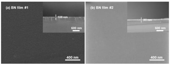
Figure 1.
Surface morphology and cross-sectional images of two Si-based BN films obtained using SEM characterization.
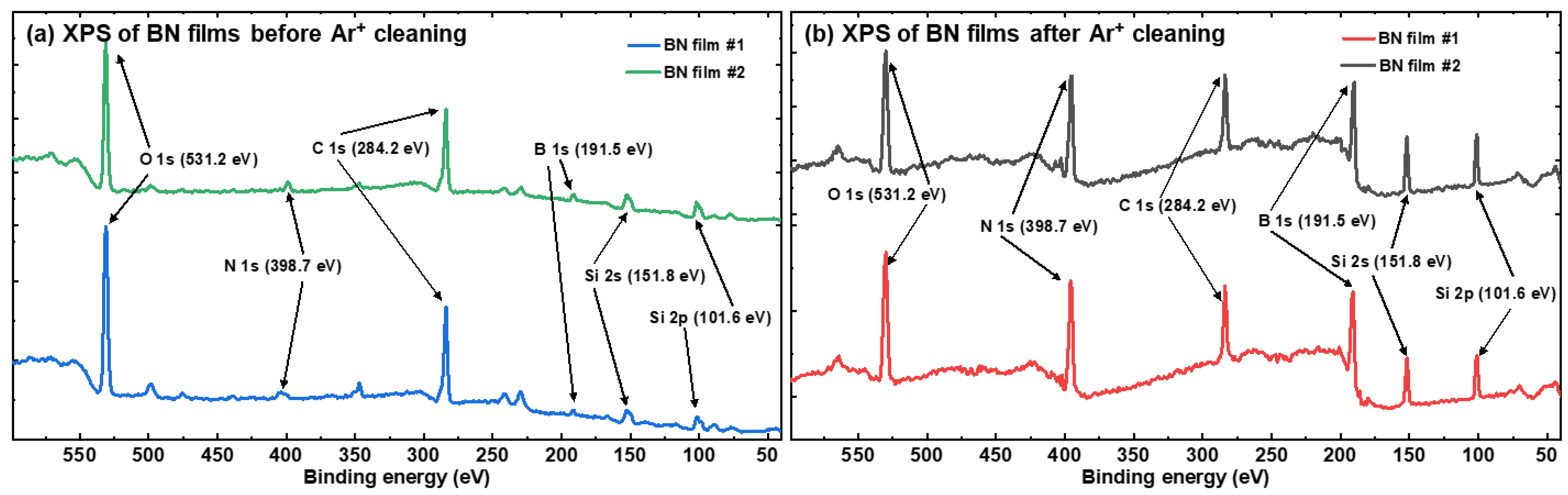
For further research on the BN film surface, we performed an X-ray photoelectron spectroscopy (XPS) analysis of the samples to distinguish the elemental composition of the sample surface. Figure 2 shows the results of the relative elemental content of the Si-based BN films characterized by XPS. From the XPS spectrum in Figure 2a, in addition to the expected N and B elements, a large amount of C and O elements are present on the film surface, which indicates the presence of surface adsorption and contamination. The results of the fine spectra of the relevant elements indicate that the film surface was contaminated with a large amount of water vapor and CO2 for a period of time (about 10 days before XPS measurement). In addition, the XPS fine spectra of the C and O elements also indicate that some C and O are present on the surface in an organic form, which suggests that there is a certain amount of organic contamination on the surface of the samples. In fact, water vapor and CO2 adsorbed on these surfaces and contaminated organic matter can have a significant effect on the surface EEC. Therefore, if a realistic BN film surface elemental composition is to be obtained, the surface needs to be cleaned with plasma to eliminate as much as possible the effects of surface adsorption and contamination on the measurement.
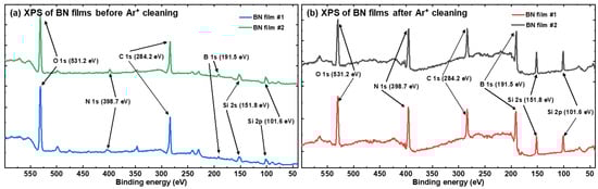
Figure 2.
Surface elemental component spectra of two silicon-based BN films obtained using XPS characterization, (a) XPS results of the original BN film without ion cleaning, (b) XPS results of the Ar-ion-cleaned BN film.
Here, we employed XPS for ion cleaning of the contaminated BN sample surface. The ion cleaning conditions were 400 eV Ar ion cleaning for 5 min at a cleaning dose of 1 μA/cm2. The XPS of the cleaned sample is shown in Figure 2b, which shows that the relative contents of B and N have increased significantly, and C and O have been effectively reduced, but there are still some residues. Therefore, the BN films prepared here should actually be considered as BN:OC films. This may be due to the fact that the preparation process was carried out only under a residual atmosphere in the high vacuum pressure range. Under these conditions, due to the high affinity of boron for oxygen, a small amount of oxygen leads to the formation of oxides. In addition, the carbon-containing gases remaining in the sputtering chamber may have a similar effect, so that the formed film also contains a certain amount of C. Hence, we refer to the samples as BN:OC films. In fact, a combination of bond energies, electronegativity differences, and actual compound properties suggests that oxygen has a stronger affinity for boron than nitrogen does for boron. This conclusion is well reflected in compound stability (e.g., the high melting point of B2O3). In any case, the effects of organic surface contamination and gas adsorption have been largely mitigated by ion cleaning. Furthermore, as can be seen in Figure 2a, the N 1s peak of film #1 is slightly larger than 400 eV. In fact, the N element peak in film #1 does not contain only N elements that are chemically combined with B, but also N elements in other forms, resulting in this peak being relatively broad. Since the surface of the sample was heavily contaminated before the ion cleaning, we believe that the prolonged storage may have led to a chemical reaction on the surface of the sample, resulting in the generation of nitrate compounds on the surface (the binding energy peak position of nitrate N 1s is near 405 eV). At the same time, due to the more serious surface contamination, the XPS fine spectroscopy analysis for individual elements could not accurately determine the specific form of this substance. From Figure 2b, we can see that the binding energy peak position of N 1s at 400 eV has disappeared after ion cleaning, indicating that the contaminants on the surface have been removed.
The EEC measurement results of the BN:OC films before and after ion cleaning are given in Figure 3, and the corresponding feature parameters of EEC curves are given in Table 1. As can be seen from Figure 3, before ion cleaning, there is a small difference in the EEC of the two BN:OC films, and the peak value of the EEC is about 3. The PE energy corresponding to the acquisition of the peak value (also noted as the most probable energy) is about 300 eV. After ion cleaning, as can be seen from Figure 3, the EEC values of the two BN:OC film samples have a significant increase in the measured PE energy range, and the peak value increases by about 0.15. This result suggests that the gas adsorption and organic contamination on the BN surface can reduce the surface EEC to a small extent.
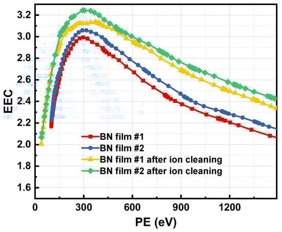
Figure 3.
EEC measurement results of two BN:OC films before and after Ar ion cleaning.

Table 1.
Statistic feature parameters of EEC curves for the BN:OC films.
2.2. Morphologic and EEC Results of BN Bulk Samples
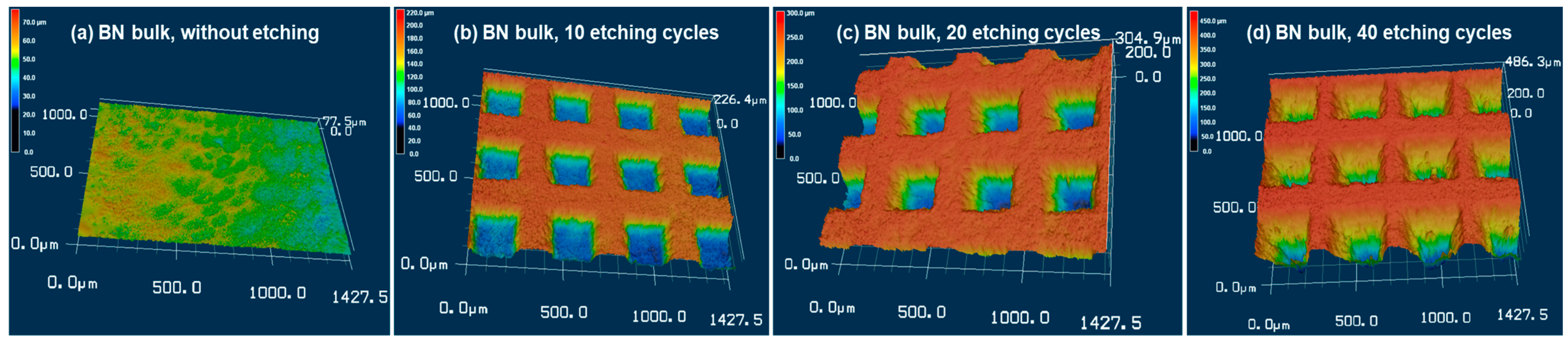
In addition to the electron emission properties of BN thin film samples, we have also investigated the electron emission properties of BN bulk samples. The BN bulk samples used here are obtained by powder sintering, and the surface etching was achieved on these BN bulk samples by laser scanning. Figure 4a shows the surface morphology of the unetched BN bulk sample in 3D form obtained by a laser scanning confocal microscope (LSCM), and this characterization result indicates that the surface roughness of the original sintered BN bulk is on the order of a few microns. In addition, to realize the EEC reduction on the surface of the BN bulk, we performed a laser etching process on the sample surface. Figure 4b–d show the 3D patterns of the microstructured BN bulk surface after laser etching (obtained by the LSCM). Via the 3D morphology of the samples, the feature sizes of the three BN microarray structures were extracted, including the side length and pore depth, and the corresponding size parameters are shown in Table 2. The aspect ratio h appearing in Table 2 is defined as the ratio of the average depth of the micropores to the pore diameter of the micropores, and the micropores aspect ratio is calculated by Equation (1),
Aspect ratio = h/b.
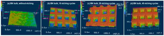
Figure 4.
(a) 3D morphology of the un-etched BN bulk and (b–d) 3D morphologies of the BN bulks treated by laser-etching 10, 20, and 40 times.
Table 2.
Statistical results of feature sizes for the laser-etched BN bulk samples.
From the test data in Table 2, it can be seen that the actual pore size of each sample is larger than the theoretical pore size, which is limited by the precision of the laser instrument (about 10 μm) and the lateral diffusion effect that occurs during the etching process. Therefore, the actual porosity of each sample is also slightly greater than the theoretical porosity. The depth h of the square pores increases significantly with the number of etching cycles, and the aspect ratio increases as well. For the laser-etched BN bulk samples, when the number of etching cycles reaches 10, as shown in Figure 4b, the bottom surface of the sample holes is relatively flat, the shape of the holes is regular, and the roughness of the hole wall is small. When the number of etching cycles reaches 20, as shown in Figure 4c, the roughness of the pore bottom and the pore wall increases significantly, and with the increase in the etching depth, the pore shape narrows gradually from the surface to the pore bottom and the structure of the pore shows a cone shape. When the number of etching cycles is further increased to 40 times, as shown in Figure 4d, the roughness of the sidewalls of the micropores increases significantly, and the 3D image shows that there is an obvious concave–convex structure in the etching area.
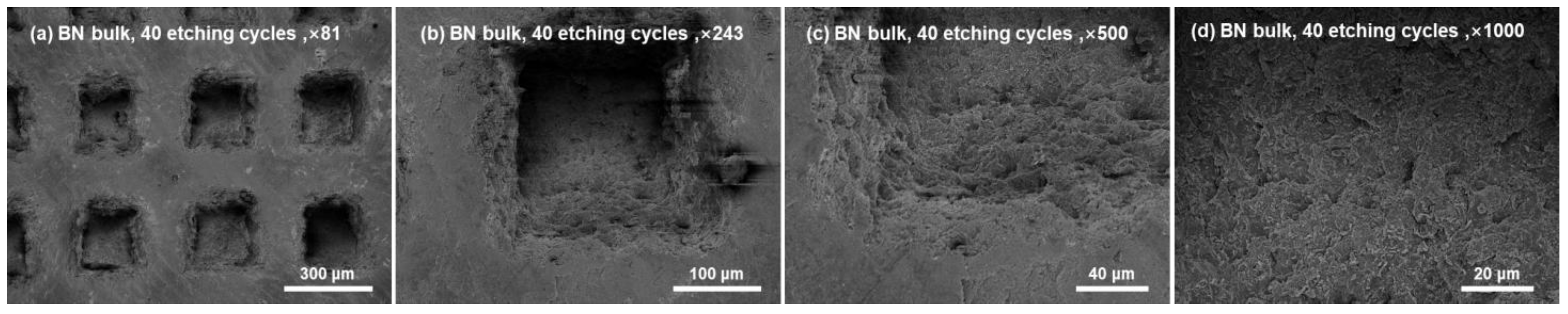
Figure 5 shows the 2D accurate surface morphology of BN bulk samples after laser etching at different magnifications. From Figure 5, it can be seen that regular microarray structures were prepared on the sample surface by laser etching, which is consistent with the LSCM characterization results in Figure 4. Additionally, the measured pore edge lengths are also consistent with the LSCM characterization results, with most of the pore edge lengths being around 250 μm, slightly exceeding the set value of 250 μm. Further observation of the morphology reveals that the surface of the un-etched area is relatively flat, especially when magnified to more than 200 times magnification. For the untreated areas shown in Figure 5, only a few small gaps and lines were generated during ceramic sintering. This can be observed in Figure 5b,c, where the surface of the unetched regions looks relatively flat. In addition, observation of the laser-etched areas of each sample, as shown in Figure 5c,d, reveals the presence of unavoidable secondary roughness on both the inner walls and edges of the etched holes, with particles of about a few micrometers in size.

Figure 5.
2D results of BN bulk (etching for 40 cycle times) surface morphology at different magnifications obtained from SEM characterization.
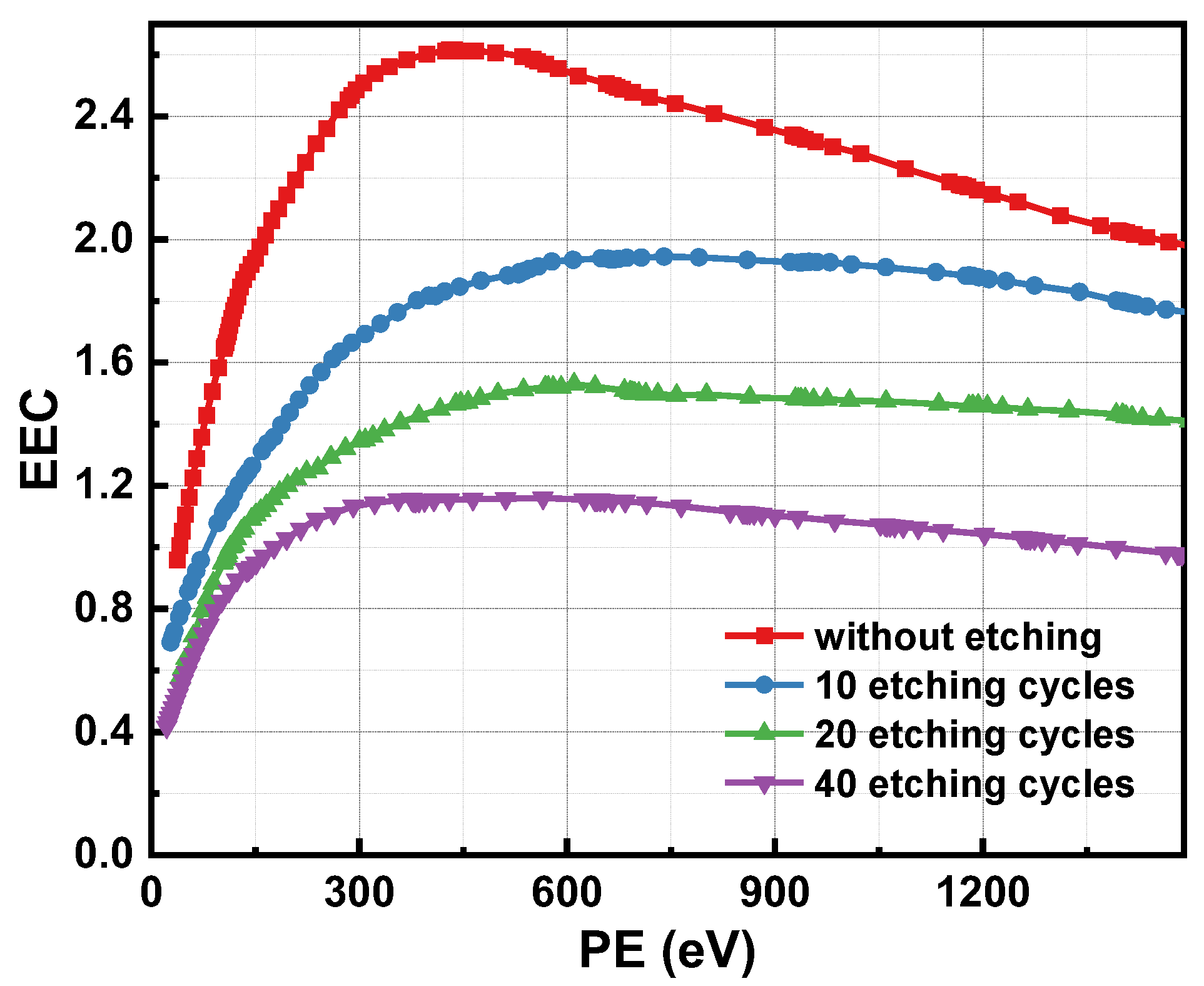
The EEC data of BN bulk samples after laser etching are given in Figure 6. The results in Figure 6 show that the microstructures formed by laser etching can significantly mitigate the electron emission behavior on the BN bulk surface and reduce the EEC in the whole measurement energy range. Typical data of the EEC curves for all samples, including the EEC peak value and the PE energy corresponding to the EEC peak value, are given in Table 3. For the unetched BN bulk samples, the EEC peak value at a PE energy of 437 eV is 2.62. After 10 times of laser etching, the EEC peak value decreases to 1.94 at a PE energy of 740 eV, which is a 26.0% decrease compared to that of untreated BN bulk. With the increase in the etching cycle, the aspect ratio increases, and the decrease rate of the EEC peak value for the BN bulk sample with 20 etching cycles increases to 41.6%, and the EEC obtains the peak value of 1.53 when the PE energy reaches 610 eV. When the number of etching cycles reaches 40, the aspect ratio of the etched microstructures reaches 1.36, and the EEC further decreases. In this case, the EEC peak value reaches 1.16, which is a decrease of more than 55.7% compared to the untreated sample, at which time the corresponding PE energy is 565 eV. Compared with the EEC data of the BN:OC film samples in Sec 2.1, we can see that the EEC of the BN bulk is relatively smaller than that of BN:OC films. Additionally, fabricating a surface microstructure array can significantly enhance the collision probability of secondary electrons with the inner wall of the microstructures, which further significantly reduces the EEC value on the BN bulk surface.
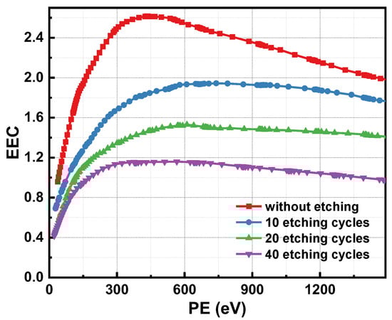
Figure 6.
Measured EEC data of the laser-etched BN bulk samples, the EEC of the untreated BN bulk sample is given as comparison.
Table 3.
Statistical results of EEC feature parameters for the laser-etched BN bulk samples.
As can be seen from Table 3, it is noteworthy that the most probable PE energy of the BN bulk samples is significantly larger than that of the BN thin film samples in Table 1. For this phenomenon, it is caused by the difference in the sample roughness on the effect of different kinds of ejected electrons. The BN thin film samples are prepared on polished silicon wafers with surface roughness on the nanometer scale. The sintered BN bulk samples have a roughness on the order of microns, while the BN bulk samples are laser etched on the surface to form microstructures with a roughness on the order of sub-millimeters. The increase in roughness increases the chance of collision of secondary electrons with the surface microstructure, and multiple collisions limit the ejection of low-energy secondary electrons. In the outgoing electrons, there is a certain proportion of backscattered electrons, which are higher in energy than the secondary electrons (comparable to the incident electrons), and the limiting effect of the microstructure on the backscattered electrons is weak. Because below the most probable PE energy, the proportion of low-energy secondary electrons is large and the proportion of backscattered electrons is small, the microstructure is able to significantly inhibit electron emission at this time. Above the most probable PE energy, the proportion of backscattered electrons gradually increases and the proportion of low-energy secondary electrons gradually decreases, so the microstructure has little effect on the emitted electrons. This results in a significant decrease in EEC below the most probable PE energy and only a small decrease in EEC above the most probable PE energy after the microstructures are prepared using the surface treatment process. Therefore, the most probable PE energy of the BN bulks is higher than that of the film samples.
2.3. Theoretical Study and Simulation of Surface Microstructure Effect on EEC
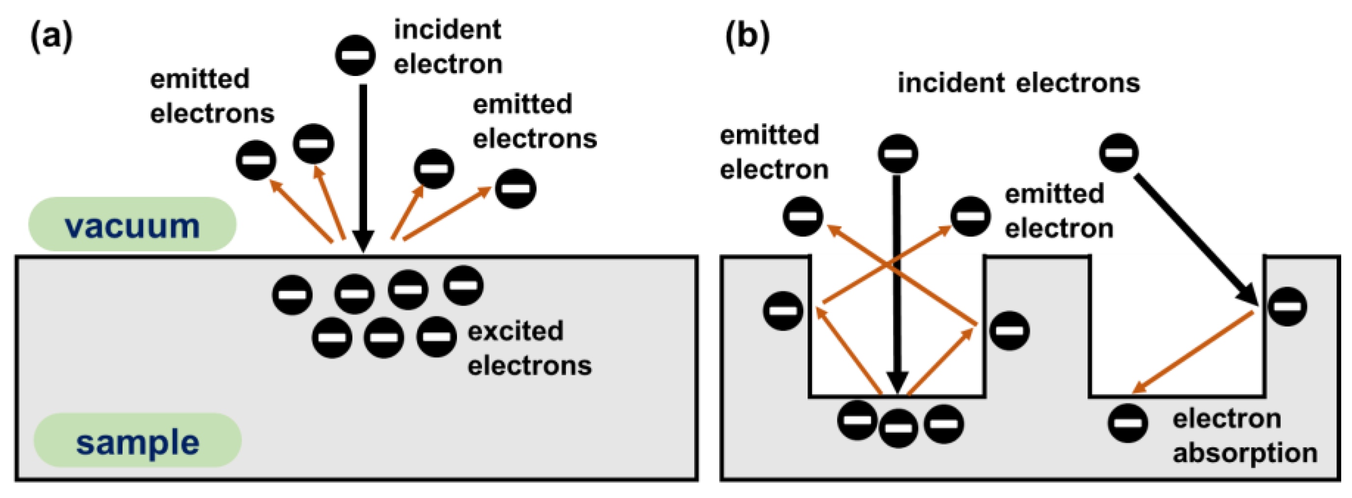
The above EEC test results in Section 2.2 show that the preparation of microarray structures on BN ceramic surfaces can effectively reduce the EEC. In fact, the physical mechanism of EEC suppression by surface microstructures is to increase the probability of collision of secondary electrons with the surface, thus limiting the emission of secondary electrons. The mechanism of EEC reduction by microstructures is discussed in detail below. Figure 7 illustrates schematic diagrams of secondary electron motion in planar structures and microstructures. In Figure 7a, the flat surface does not have sidewall structures that impede the emission of electrons, so secondary electrons excited by primary electrons can escape the surface unimpeded. However, in the microstructure, the trap sidewalls block the first generation of outgoing electrons, resulting in most of the secondary electrons colliding with the sidewalls, as shown in Figure 7b. In microstructures, due to the low energy of the secondary electrons (typically a few eV), these electrons colliding with the sidewalls are most likely absorbed by the material and cannot escape from the microstructure. A small number of secondary electrons with slightly higher energies (a few tens of eV) will collide with the sidewall again, possibly exciting more secondary electrons. If these secondary electrons are orientated towards the exit of the microstructure, they will escape. Otherwise, they will continue to collide with the microstructure wall and will most likely be absorbed by the material due to the low energy.
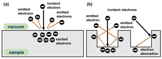
Figure 7.
Schematic diagram of internal electron emission induced by electron incident on a solid surface, (a) untreated flat surface, (b) surface with microstructures.
In order to theoretically verify the effect of microstructures on the EEC of a BN bulk sample, we use a phenomenological model of secondary electrons combined with an electron tracking algorithm to compute the EEC of the microstructures. So far, several researchers have developed modeling theories for calculating the EEC for some typical materials [35,36,37,38] or estimating the electron scattering process [39,40]. The regular geometric array shown in Figure 4 is used as an equivalent of the actual microstructures, and the geometrical parameters of the equivalent model are chosen to be the sizes shown in Table 2. The simulation process can be briefly described as follows. First, the EEC of the pristine BN surface is simulated using the MEST model [35] by MATLAB (2021b) to determine some necessary parameters. Second, based on the determined parameters, the electron incidence and emission conditions of the collision event are simulated using the Monte Carlo method. Third, the motion of the electrons on the surface of the microstructures is simulated based on the electron tracking algorithm. Fourth, the final state of the electrons during their movement (escaping from the surface or colliding with the microarray structure again) is determined. Fifth, we repeat the second to fourth processes above until all electron collisions have been simulated. For each structure, the number of incident electrons was set to 50,000 to ensure the accuracy of the simulation results as much as possible.
We calculated the EEC for the case of different aspect ratios on the BN bulk surface using the simulation method described above. The data for the three aspect ratios are extracted from Table 2 and are 0.44, 0.86, and 1.36, respectively. The simulation results in Figure 8 show that the EEC decreases gradually with the increase in aspect ratio. This simulation result indicates that the blocking effect of the microstructure on the electron motion gradually increases, limiting the electron ejection. The simulation results of EEC in Figure 8 are in agreement with the experimental test results in Figure 6, which verifies the effect regularity of the microstructure aspect ratio on the surface EEC for the BN bulk samples.
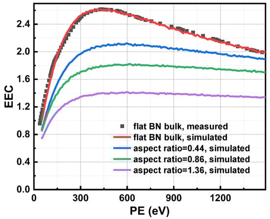
Figure 8.
The simulation obtained the trend of the effect of microstructure on the surface EEC, in the case where the aspect ratio of the microstructure was varied (refer to the real aspect ratio values in Table 2).
3. Materials and Methods
3.1. BN Film Preparation
In the preparation experiments, thin film deposition was carried out using radio frequency magnetron sputtering. The N-type heavily doped monocrystalline silicon wafers are employed as substrates (crystal orientation 100, resistivity less than 1 × 10⁻³ Ω·m). All substrates were cleaned sequentially with acetone, alcohol, and ultrapure water to remove any possible contaminants on the substrate surface. The sputtering source used in the experiments was a commercially available BN compound target (76.2 mm in diameter and 5 mm in thickness), and the purity of the BN ceramic target is 99.99%. The gas pressure in the vacuum chamber was pumped down to less than 3 × 10⁻⁴ Pa before the experiments to ensure that the sputtering process was as free as possible from other residual gases. High-purity argon (Ar, 99.99% pure) was introduced as the working gas during the experiments. During the sputtering process, the Ar pressure in the chamber was controlled using a gas flow meter. The substrates were not heated during the sputtering process, the sputtering time was 120 min, the sputtering power was 100 W, the gas flow of Ar was 15 sccm, and the gas pressure in the chamber was controlled at 1.2 Pa. Two samples were fabricated by employing the same sputtering parameters, and they were denoted as BN film #1 and #2, respectively.
3.2. BN Bulk Etching Method
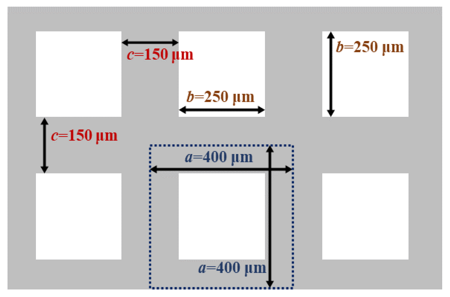
Surface etching for the BN bulk samples was implemented in the atmospheric environment. The BN bulks originate from the ceramic sintering process, which is separately prepared. The diameter of the BN bulk samples is 50 mm, and the thickness is 5 mm. A pulsed infrared fiber laser was employed to etch the samples to construct the surface microarray structure for EEC modulation. The parameters of the laser facility are as follows: the laser wavelength is 1064 nm, the focal length is about 150 mm, and the maximum etching power is 20 W. The etching parameter we used in preparing the microarray structures is 40 J/cm2. Arrayed square microstructures were achieved on the sample surface, as shown in Figure 9. Each etching unit within the microarray is also depicted, where b represents the side length of the square hole, a represents the side length of the etching unit, and c represents the offset distance between adjacent square holes. Three sets of square hole microarray structures with different hole depths were prepared by controlling the processing number of single points to modulate the etching depth. The processing parameters for each sample are as follows. The square length b is 250 μm, the side length of each unit a is 400 μm, and the offset distance c is 150 μm. The cycle numbers of laser etching were set to 10, 20, and 40 for the three BN bulk samples, respectively. The theoretical porosity is defined as the ratio of the projected area of the etched region within the unit cell to the total projected area of the unit cell, denoted as P. For the etching pattern in Figure 9, the theoretical porosity is determined by Equation (2),
P = b2/a2,
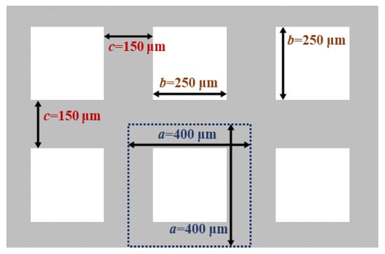
Figure 9.
Schematic diagram of the surface etching of a BN bulk, including a side length of the etching unit a, a square graphic and its side length b of the etching, and an offset distance c of the neighboring etching graphic.
3.3. Physical Characterization Methods
In the characterization experiments, the surface morphology as well as the cross-sectional images of the prepared film samples were characterized using an SEM (Zessi Gemini 500, Oberkochen, Germany). The 3D morphologies of the square hole microarray structures were characterized by an LSCM (Keyence VK9700, Osaka, Japan). For the characterization of the surface element composition of the fabricated BN film, XPS was employed (made by Thermo Fisher, ESCALAB Xi+, Al Kα, Waltham, MA, USA). In addition to elemental characterization for relatively cleaning surfaces, we also cleaned the surface of the BN thin film samples with XPS to remove surface adsorption and contaminations. In the experiment, the sample surface was cleaned using an argon ion beam stream with an energy of 1000 eV for a duration of 30 min. EEC measurements are performed using a self-developed system equipped with two neutralization guns to eliminate surface charge build-up. Due to the poor electrical conductivity of dielectric materials, charge build-up occurs when electrons bombard the surface, thus affecting accurate EEC measurements. Therefore, surface charge neutralization is used for EEC measurements. The exact principle of the EEC measurement method can be found in the reference [41].
4. Conclusions
In this work, we focus on the electron emission properties of BN materials. The electron emission behavior of BN thin films and BN bulk samples as influenced by the surface state was investigated. The following conclusions can be obtained from the study. First, the BN film surface obtained by sputtering is susceptible to gas adsorption and organic contamination, resulting in surface condition modification, and further leading to a slight decrease in surface EEC, with an EEC peak value of about 3.0 at about 300 eV PE energy. Second, ion cleaning is effective in removing the adsorbed gases and contaminated organic impurities on the BN film surface, and the EEC peak value rises to about 3.2 after ion cleaning. Third, the roughness of the sintered BN ceramic bulk is on the order of a few micrometers, and the EEC peak value of the BN bulk is about 2.62. Fourth, the EEC of the laser-etched BN bulk is significantly reduced, for the BN bulk etched by laser 40 times, its aspect ratio is 1.36 and the EEC peak value is about 1.16. The mechanism of the microstructure’s effect on EEC has been analyzed by explaining the electron collisions with microstructure surfaces. In this work, a detailed study was carried out to investigate the surface electron emission characteristics of the BN thin films and the BN bulks. The results are valuable for engineering applications of vacuum electronic devices applying BN as a functional layer or support material.
Author Contributions
Conceptualization, D.W.; methodology, Y.G. and D.W.; software, Y.G.; validation, Y.G. and J.L.; formal analysis, Y.G.; investigation, Y.G.; resources, J.L.; data curation, Y.G. and D.W.; writing—original draft preparation, Y.G. and D.W.; writing—review and editing, D.W.; visualization, Y.G.; supervision, D.W. and J.L.; project administration, J.L.; funding acquisition, Y.G. All authors have read and agreed to the published version of the manuscript.
Funding
This work was supported by the Project of Science and Technology Research Program of Chongqing Education Commission of China (No. KJQN202303210) and the Project of Science and Technology Research Program of Chongqing Education Commission of China (No. KJQN202403217).
Institutional Review Board Statement
Not applicable.
Informed Consent Statement
Not applicable.
Data Availability Statement
The original contributions presented in the study are included in the article, further inquiries can be directed to the corresponding authors.
Conflicts of Interest
The authors declare no conflicts of interest.
References
- Shayeganfar, F.; Shahsavari, R. Electronic and pseudomagnetic properties of hybrid carbon/boron-nitride nanomaterials via ab-initio calculations and elasticity theory. Carbon 2016, 99, 523–532. [Google Scholar]
- Zhou, J.; Wang, Q.; Sun, Q.; Jena, P. Electronic and magnetic properties of a BN sheet decorated with hydrogen and fluorine. Phys. Rev. B 2010, 81, 085442. [Google Scholar]
- Bello, I.; Chan, C.Y.; Zhang, W.J.; Chong, Y.M.; Leung, K.M.; Lee, S.T.; Lifshitz, Y. Deposition of thick cubic boron nitride films: The route to practical applications. Diam. Relat. Mater. 2005, 14, 1154–1162. [Google Scholar] [CrossRef]
- Levchenko, I.; Xu, S.; Teel, G.; Mariotti, D.; Walker, M.L.R.; Keidar, M. Recent progress and perspectives of space electric propulsion systems based on smart nanomaterials. Nat. Commun. 2018, 9, 879. [Google Scholar] [CrossRef]
- Barral, S.; Makowski, K.; Peradzynski, Z.; Gascon, N.; Dudeck, M. Wall material effects in stationary plasma thrusters. II. Near-wall and in-wall conductivity. Phys. Plasmas 2003, 10, 4137–4152. [Google Scholar]
- Burton, T.; Schinder, A.M.; Capuano, G.; Rimoli, J.J.; Walker, M.L.R.; Thompson, G.B. Plasma-induced erosion on wall structures in Hall-effect thrusters. J. Propul. Power 2014, 30, 690–695. [Google Scholar]
- Meezan, N.B.; Gascon, N.; Cappelli, M.A. Linear geometry Hall thruster with boron nitride and diamond walls. In Proceedings of the 27th International Electric Propulsion Conference, Pasadena, CA, USA, 15–19 October 2001. [Google Scholar]
- Lian, Z.X.; Li, D.J.; Wang, D.; He, Y.N. Discharge characteristics of the planar microscale gap electrodes with various geometry structures in the atmosphere environment. Results Phys. 2024, 62, 107823. [Google Scholar] [CrossRef]
- Gascon, N.; Dudeck, M.; Barral, S. Wall material effects in stationary plasma thrusters. I. Parametric studies of an SPT-100. Phys. Plasmas 2003, 10, 4123–4136. [Google Scholar]
- Locke, S.; Shumlak, U.; Fife, J.M. A Numerical Study of the Effect of Channel Insulator Discontinuity on Hall Thruster Discharge. In Proceedings of the 27th International Electric Propulsion Conference, Pasadena, CA, USA, 15–19 October 2001. [Google Scholar]
- Chang, H.Y.; Alvarado, A.; Weber, T.; Marian, J. Monte Carlo modeling of low-energy electron-induced secondary electron emission yields in micro-architected boron nitride surfaces. Nucl. Instrum. Methods B 2019, 454, 14–22. [Google Scholar]
- Lian, Z.X.; Xu, Y.N.; Meng, X.C.; Wang, D.; Chen, J.X.; Qi, K.C.; He, Y.N. Secondary electron emission reduction from boron nitride composite ceramic surfaces by the artificial microstructures and functional coating. J. Phys. D Appl. Phys. 2024, 57, 315304. [Google Scholar]
- Seiler, H. Secondary electron emission in the scanning electron microscope. J. Appl. Phys. 1983, 54, R1–R18. [Google Scholar]
- Lee, J.; Jeong, T.; Yu, S.G.; Jin, S.; Heo, J.; Yi, W.; Jeon, D.; Kim, J.M. Thickness effect on secondary electron emission of MgO layers. Appl. Surf. Sci. 2001, 174, 62–69. [Google Scholar]
- Lian, Z.X.; Zhu, X.P.; Wang, D.; Meng, X.C.; He, Y.N. Effect of atmospheric environment on the stability of secondary electron emission from magnesium oxide and alumina surfaces. J. Phys. D Appl. Phys. 2023, 57, 125302. [Google Scholar]
- Cazaux, J. Calculated influence of work function on SE escape probability and Secondary Electron Emission yield. Appl. Surf. Sci. 2010, 257, 1002–1009. [Google Scholar]
- Gineste, T.; Belhaj, M.; Teyssedre, G.; Puech, J. Investigation of the electron emission properties of silver: From exposed to ambient atmosphere Ag surface to ion-cleaned Ag surface. Appl. Surf. Sci. 2015, 359, 398–404. [Google Scholar]
- Fijol, J.J.; Then, A.M.; Tasker, G.W.; Soave, R.J. Secondary-electron yield of SiO2 and Si3N4 thin-films for continuous dynode electron multipliers. Appl. Surf. Sci. 1991, 48–49, 464–471. [Google Scholar]
- Lapington, J.S.; Thompson, D.P.; May, P.W.; Fox, N.A.; Howorth, J.; Milnes, J.; Taillandier, V. Investigation of the secondary emission characteristics of CVD diamond films for electron amplification. Nucl. Instrum. Methods A 2009, 610, 253–257. [Google Scholar]
- Cimino, R.; Collins, I.R.; Furman, M.A.; Pivi, M.; Ruggiero, F.; Rumolo, G.; Zimmermann, F. Can Low-Energy Electrons Affect High-Energy Physics Accelerators? Phys. Rev. Lett. 2004, 93, 014801. [Google Scholar]
- Le Pimpec, F.; Kirby, R.E.; King, F.K.; Pivi, M. The effect of gas ion bombardment on the secondary electron yield of TiN, TiCN and TiZrV coatings for suppressing collective electron effects in storage rings. Nucl. Instrum. Methods A 2006, 564, 44–50. [Google Scholar]
- Hueso, J.; Vicente, C.; Gimeno, B.; Boria, V.E.; Marini, S.; Taroncher, M. Multipactor Effect Analysis and Design Rules for Wedge-Shaped Hollow Waveguides. IEEE Trans. Electron Dev. 2010, 57, 3508–3517. [Google Scholar]
- Meng, X.C.; Xu, Y.N.; Lian, Z.X.; Wang, J.Y.; Wang, D.; Qi, K.C. Secondary roughness effect of surface microstructures on secondary electron emission and multipactor threshold for PTFE-filled and PI-filled single ridge waveguides. J. Phys. D Appl. Phys. 2024, 57, 265301. [Google Scholar] [CrossRef]
- Pivi, M.; King, F.K.; Kirby, R.E.; Raubenheimer, T.O.; Stupakov, G.; Le Pimpec, F. Sharp reduction of the secondary electron emission yield from grooved surfaces. J. Appl. Phys. 2008, 104, 104904. [Google Scholar] [CrossRef]
- Watts, C.; Gilmore, M.; Schamiloglu, E. Effects of laser surface modification on secondary electron emission of copper. IEEE Trans. Plasma Sci. 2011, 39, 836–841. [Google Scholar] [CrossRef]
- Nistor, V.; González, L.A.; Aguilera, L.; Montero, I.; Galán, L.; Wochner, U.; Raboso, D. Multipactor suppression by micro-structured gold/silver coatings for space applications. Appl. Surf. Sci. 2014, 315, 445–453. [Google Scholar] [CrossRef]
- Montero, I.; Mohamed, S.H.; García, M.; Galán, L.; Raboso, D. Effect of surface reactions of low-energy carbon ions on the secondary electron emission of TiN:O thin films. J. Appl. Phys. 2007, 101, 113306. [Google Scholar] [CrossRef]
- Lian, Z.X.; Wang, D.; Zhu, X.P.; He, Y.N. High-performance microchannel plates based on atomic layer deposition for the preparation of functional layers. J. Phys. D Appl. Phys. 2025, 58, 115106. [Google Scholar] [CrossRef]
- Henrist, B.; Hilleret, N.; Scheuerlein, C.; Taborelli, M. The secondary electron yield of TiZr and TiZrV non-evaporable getter thin film coatings. Appl. Surf. Sci. 2001, 172, 95–102. [Google Scholar] [CrossRef]
- Prodanovic, V.; Chan, H.W.; Mane, A.U.; Elam, J.W.; Minjauw, M.M.; Detavernier, C.; Harry, V.D.G.; Sarro, P.M. Effect of thermal annealing and chemical treatments on secondary electron emission properties of atomic layer deposited MgO. J. Vac. Sci. Technol. A 2018, 36, 06A102. [Google Scholar] [CrossRef]
- Ruiz, A.; Román, E.; Lozano, P.; García, M.; Galán, L.; Montero, I.; Raboso, D. UHV reactive evaporation growth of titanium nitride thin films, looking for multipactor effect suppression in space applications. Vacuum 2007, 81, 1493–1497. [Google Scholar] [CrossRef]
- Thomas, S.; Pattinson, E.B. The controlled preparation of low SEE surfaces by evaporation of metal films under high residual gas pressures. J. Phys. D Appl. Phys. 1970, 3, 1469–1474. [Google Scholar] [CrossRef]
- Valizadeh, R.; Malyshev, O.B.; Wang, S.; Zolotovskaya, S.A.; Allan Gillespie, W.; Abdolvand, A. Low secondary electron yield engineered surface for electron cloud mitigation. Appl. Phys. Lett. 2014, 105, 231605. [Google Scholar]
- Dunaevsky, A.; Raitses, Y.; Fisch, N.J. Secondary electron emission from dielectric materials of a Hall thruster with segmented electrodes. Phys. Plasmas 2003, 10, 2574–2577. [Google Scholar]
- de Lara, J.; Pérez, F.; Alfonseca, M.; Galán, L.; Montero, I.; Román, E.; Garcia-Baquero, D.R. Multipactor prediction for on-board spacecraft RF equipment with the MEST software tool. IEEE Trans. Plasma. Sci. 2006, 34, 476–484. [Google Scholar]
- Vaughan, J.R. A new formula for secondary emission yield. IEEE Trans. Electron. Dev. 1989, 36, 1963–1967. [Google Scholar]
- Furman, M.A.; Pivi, M. Probabilistic model for the simulation of secondary electron emission. Phys. Rev. Spec. Top.-Accel. Beams 2002, 5, 124404. [Google Scholar]
- Dionne, G.F. Effects of secondary electron scattering on secondary emission yield curves. J. Appl. Phys. 1973, 44, 5361–5364. [Google Scholar]
- Young, J.R. Penetration of electrons and ions in aluminum. J. Appl. Phys. 1956, 27, 1–4. [Google Scholar]
- Lane, R.O.; Zaffarano, D.J. Transmission of 0–40 keV electrons by thin films with application to beta-ray spectroscopy. Phys. Rev. 1954, 94, 960–964. [Google Scholar]
- Cai, Y.H.; Wang, D.; Qi, K.C.; He, Y.N. Measurement of total electron emission yield of insulators based on self-terminating charge neutralization. Rev. Sci. Instrum. 2022, 93, 055103. [Google Scholar]


Disclaimer/Publisher’s Note: The statements, opinions and data contained in all publications are solely those of the individual author(s) and contributor(s) and not of MDPI and/or the editor(s). MDPI and/or the editor(s) disclaim responsibility for any injury to people or property resulting from any ideas, methods, instructions or products referred to in the content. |
© 2025 by the authors. Licensee MDPI, Basel, Switzerland. This article is an open access article distributed under the terms and conditions of the Creative Commons Attribution (CC BY) license (https://creativecommons.org/licenses/by/4.0/).