Abstract
KNbO3 single crystals are grown by the self-flux method using K2CO3 as a flux, but often suffer from discolouration. In this work, KNbO3 single crystals were grown by the flux method using KBO2 as a flux. KNbO3 powder was prepared by the solid-state reaction of K2CO3 and Nb2O5. KBO2 was fabricated by the reaction of K2B4O7·4H2O and K2CO3. Single crystals of KNbO3 were grown in a Pt crucible and the structure and dielectric properties of the single crystals were investigated. X-ray diffraction showed the KNbO3 single crystals to have an orthorhombic Cmm2 perovskite unit cell at room temperature. The existence of ferroelastic domains was revealed by transmission electron microscopy. Electron probe microanalysis showed the single crystals to be stoichiometric and contain small amounts of B. Differential thermal analysis, Raman scattering and impedance spectroscopy were used to study the phase transitions. KBO2 may be a suitable flux for the growth of KNbO3 single crystals.
1. Introduction
KNbO3 is a ferroelectric perovskite material with an orthorhombic perovskite unit cell (Amm2 or Bmm2) at room temperature [1,2]. KNbO3 undergoes a rhombohedral (R3m) to orthorhombic phase transition at ~−10 °C, an orthorhombic to tetragonal (P4mm) phase transition at ~225 °C and a tetragonal to cubic (Pmm) phase transition at ~435 °C [2,3,4]. KNbO3 is an end member of the KNbO3-NaNbO3 pseudo-binary system [5,6], which is an important system for future lead-free piezoelectric applications [7,8]. Undoped KNbO3 ceramics and KNbO3 ceramics co-doped with La and Fe have moderate piezoelectric properties (d33 = 98–114 pC/N, k33 = 0.49, kp = 0.17–0.25, kt = 0.18–0.48) [9,10,11,12,13] and the properties of KNbO3 can be adapted by forming solid solutions [14] or by using CuO as a sintering aid [15].
Single crystals of KNbO3 are of interest for their high value of kt (0.69), low density (4.62 g/cm3), high acoustic velocity (7800 m/s) and low clamped relative permittivity (εS = 28–42), which make them suitable for transducers [16,17,18,19,20,21]. Single crystals of KNbO3 are also of interest for their nonlinear optical properties such as second harmonic generation [22,23,24,25]. KNbO3 melts incongruently, so single crystals are impossible to grow from a melt of KNbO3 composition [21,26]. Single crystals of KNbO3 have been grown by the self-flux method, Bridgman method and by top-seeded solution growth usually with addition of excess K2O or K2CO3 [21,27,28,29,30,31,32,33]. Single crystals of KNbO3 grown by these methods often show a blue colour which is detrimental to the optical properties [28,31,32,33]. This colouration is believed to be caused by oxygen vacancies [32,34] or Rayleigh scattering [35] and can be avoided by careful control of the K2O/K2CO3 excess, soaking temperature or starting temperature for growth [28,32,33].
Borates are commonly used as a flux to grow single crystals by the flux growth method [36,37]. Na2B4O7 and NaBO2 have been used as fluxes to grow single crystals of NaNbO3 [38,39]. Rudkovskaya et al. found that KNbO3 and KBO2 form a simple binary eutectic system with a eutectic point at 73 mol % KBO2 and 860 °C [40,41,42]. In the present study, KBO2 is used as a flux for the growth of KNbO3 single crystals for the first time and the structure, phase transitions and dielectric properties of the single crystals are investigated. The results from this work show that, as suggested by Rudkovskaya et al. [40,41,42], KBO2 may be a suitable flux for the growth of KNbO3 single crystals.
2. Results
An X-ray diffraction (XRD) pattern of the calcined KNbO3 powder is shown in Figure 1. The pattern can be indexed with Crystallography Open Database pattern #96-231-0012 for KNbO3 (orthorhombic, space group Bmm2). There are some peaks of a secondary phase which can be indexed with Crystallography Open Database pattern #96-100-1843 for K4Nb6O17.
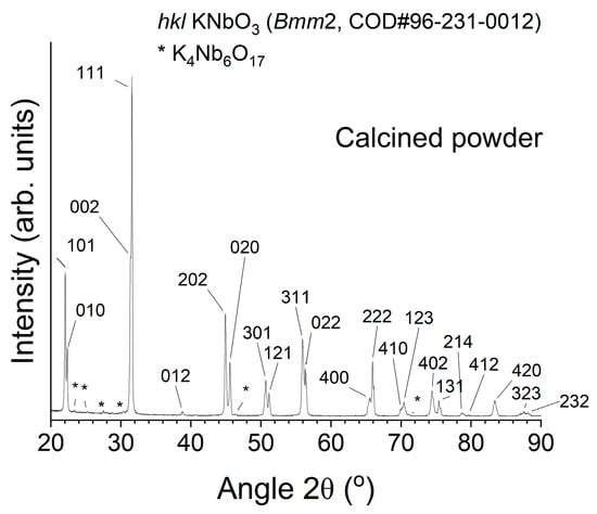
Figure 1.
XRD pattern of calcined KNbO3 powder.
Single crystals inside the Pt crucible immediately after growth are shown in Figure 2a. Single crystals appear to have grown on the crucible walls. Single crystals after removal from the crucible and cleaning are shown in Figure 2b. Each crystal is labelled with a number 1–3 for reference. Single crystals up to ~15 × 15 mm in size have grown. Single crystal 2 is actually several single crystals which have grown into each other. Some of the edges of the single crystals are blue in colour. The white colour in the bulk of the crystals may be caused by scattering of light by ferroelectric domains [43]. As a consequence of the use of the flux method, single crystals were grown freely without thermal or mechanical stresses, which allowed the development of natural growth facets [44].
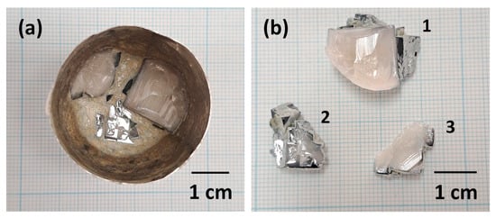
Figure 2.
Pictures of KNbO3 single crystals: (a) inside the Pt crucible immediately after growth; (b) after removal from the crucible and cleaning. Each crystal in (b) is labelled with a number 1−3 for reference.
XRD patterns of bulk and powder samples of the KNbO3 single crystals are shown in Figure 3. The XRD patterns of the bulk samples (labelled single crystals 2a and 2b) are obtained from single crystals separated from single crystal 2 in Figure 2b. The patterns in Figure 3a can be indexed with Crystallography Open Database pattern #96-231-0012 for KNbO3 (orthorhombic, space group Bmm2). Peak positions and d-spacings of the crystallographic planes which show strong reflections are given in Table 1. The 101 and 202 reflections of the bulk single crystal 2a are very strong, with weaker 010, 020 and 303 reflections also present. The 101 and 202 reflections of the bulk single crystal 2b are also very strong. The relative intensity of the 010 and 020 reflections in single crystal 2b are stronger than those of single crystal 2a. The 202 and 020 reflections of each crystal are shown in detail in the insets. The peaks in single crystal 2b are noticeably broader than those in single crystal 2a. A weak 111 reflection is also present in the pattern of single crystal 2b. The small differences in peak position and d-spacing between the two crystals indicate that they have slightly different unit cell parameters. There are weak peaks in the pattern for single crystal 2a which belong to a secondary phase, possibly K2B4O7 or K3B2Nb3O12. These peaks may come from a secondary phase inclusion in the crystal or from flux remaining on the crystal surface.
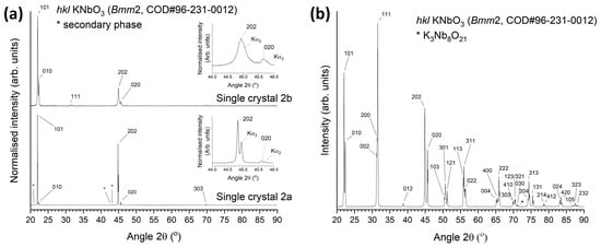
Figure 3.
XRD patterns of KNbO3 single crystals: (a) bulk samples; (b) powder sample.

Table 1.
Peak positions and d-spacings of the crystallographic planes of the single crystals in Figure 3a.
For an X-ray diffractometer in Bragg–Brentano geometry, X-rays can only be diffracted by crystallographic planes parallel to the sample surface [45]. Intense peaks appear only from parallel h0l and 0k0 crystallographic planes in the pattern of single crystal 2a, indicating that the sample really is a single crystal. The appearance of the 010 and 020 reflections indicates the existence of non-180° ferroelectric/ferroelastic domains [46,47,48]. Single crystal 2b also contains intense 101 and 202 reflections, indicating that it also is a single crystal or at least contains a single crystal. The weak 111 reflection in the pattern of single crystal 2b may come from a single crystal aligned at a different angle. The difference in relative intensities of the h0l/0k0 peak pairs indicates that different single crystals may have different domain structures.
The pattern of the crushed KNbO3 single crystal powder sample in Figure 3b can also be indexed with Crystallography Open Database pattern #96-231-0012. A minor peak belonging to a K3Nb8O21 secondary phase (Crystallography Open Database pattern #96-100-1028) is present. This peak may come from a secondary phase inclusion in the crystal or from flux remaining on the crystal surface.
A diffraction pattern of a KNbO3 single crystal obtained using single crystal XRD is shown in Figure 4. This is the same single crystal as single crystal 2a in Figure 3a. The diffraction pattern shows that the sample really is a single crystal. Unit cell parameters of the KNbO3 single crystal are given in Table 2. The single crystal is orthorhombic with Cmm2 space group. The results can be summarised as follows: M = 180.01 g/mol, orthorhombic, space group Cmm2 (no. 35), a = 5.660 (1) Å, b = 5.664(1) Å, c = 4.027(1) Å, V = 129.09(5) Å3, Z = 2, T = 296(2) K, μ(MoKα) = 6.008 mm−1, Dcalc = 4.631 g/cm3, 652 reflections measured (10.126° ≤ 2Θ ≤ 52.708°) and 156 unique (Rint = 0.0191, Rsigma = 0.0166) which were used in all calculations. The final R1 was 0.0356 (I > 2σ(I)) and wR2 was 0.0920 (all data). This information is available on the Crystallography Open Database (entry 3000498). The unit cell parameters are different to those previously obtained by Shirane et al. [3], being more elongated along the c axis and compressed along the a and b axes. This may be caused by incorporation of B into the crystal lattice.
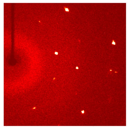
Figure 4.
Diffraction pattern of a KNbO3 single crystal taken by single crystal XRD.

Table 2.
Unit cell parameters of a KNbO3 single crystal.
Electron probe microanalysis (EPMA) results of two KNbO3 single crystal samples are shown in Table 3. The results are given as the mol % of each constituent oxide in the single crystal. Each value is the mean and standard deviation of ten point measurements. Normalised to two moles of cations, the composition of sample 1 is K1.000±0.004Nb0.995±0.004B0.005±0.006O3 and the composition of sample 2 is K0.971±0.006Nb0.997±0.010B0.033±0.012Al0.0002±0.0003O3. Both samples have compositions close to the nominal composition for KNbO3. Both samples contain B. B was detected at all ten point measurements in the second sample, so it appears to be evenly distributed throughout the crystal rather than appearing in a flux inclusion. The second sample contains only a trace amount of Al, so contamination with Al during processing (e.g., from the alumina crucible during calcination) is not an issue. The difference in composition of the two crystals may be the cause of the differences in XRD peak position and d-spacing (Table 1).

Table 3.
EPMA results of two KNbO3 single crystal samples.
Transmission electron microscopy (TEM) micrographs of a KNbO3 single crystal are shown in Figure 5. Figure 5a shows that the single crystal contains lamellar domains of up to 1 μm thickness aligned on (110)pc crystallographic planes, where pc means pseudo-cubic. The corresponding selected area electron diffraction (SAED) pattern is shown in Figure 5b, indexed using a pseudo-cubic unit cell. Splitting of the 222 spot (marked with a blue box) in the [110]pc direction can be seen. For a crystal with orthorhombic symmetry, 90° domain walls lie on (100) planes while 180° domain walls, uncharged 120° domain walls and charged 60° domain walls lie on (110) planes [49]. The presence of splitting in the [110]pc direction in Figure 5b indicates that the domain walls are ferroelastic 120° or 60° domain walls, as 180° domain walls do not exhibit splitting. Figure 5c is a scanning transmission electron microscopy (STEM) dark-field image of the tips of the domains. Smaller nanoscale domains have formed at the domain tips (marked with white arrows). Figure 5d reveals stresses of a higher magnitude localised at the lamellar domain walls and at the domain tips.
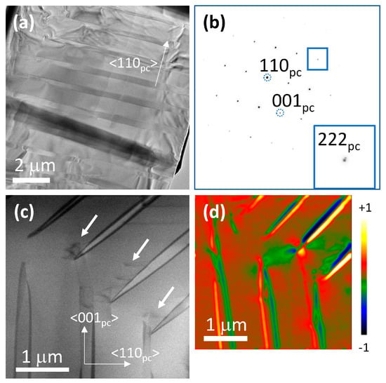
Figure 5.
(a) TEM micrograph of a KNbO3 single crystal; (b) corresponding SAED pattern showing the splitting of the 222 spot in the [110]pc direction; (c) STEM dark-field image of the tips of the domains, white arrows mark nanoscale domains; (d) divergence image obtained from 4D STEM dataset show larger contrast changes at domain walls. The numbers +1 and −1 are arbitrary units, showing the maximum and minimum changes in strain.
An atomic resolution high-angle annular dark-field (HAADF) STEM image in the [110]pc zone axis [Figure 6a] shows brighter Nb and darker K atom columns. No cation-related defects are visible within the analysed region. The Integrated Differential Phase Contrast (iDPC) image in the [110]pc zone axis is shown in Figure 6b, along with corresponding energy dispersive X-ray spectroscopy (EDXS) analysis [Figure 6c] and crystallographic model [Figure 6d], confirming a homogeneous distribution of all elements and an orthorhombic structure within the analysed area.
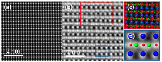
Figure 6.
(a) HAADF-STEM and (b) iDPC images of KNbO3 in the [110]pc zone axis with corresponding (c) atomic scale EDXS analysis (corresponding to the red frame in (b,d) orthorhombic KNbO3 crystallographic model (ICSD:01-077-1098) (corresponding to the blue frame in (b)) depicting the positions of K (blue), Nb (red), and O (green).
A differential thermal analysis (DTA) trace of a KNbO3 single crystal powder sample is shown in Figure 7. The trace shows endothermic peaks with onsets at 217 °C and 425 °C on heating. These peaks correspond to the orthorhombic–tetragonal and tetragonal–cubic phase transitions, respectively. Exothermic peaks at 416 °C and 198 °C on cooling correspond to the cubic–tetragonal and tetragonal–orthorhombic phase transitions. The phase transitions show temperature hysteresis, indicating that they are first-order [4,50].
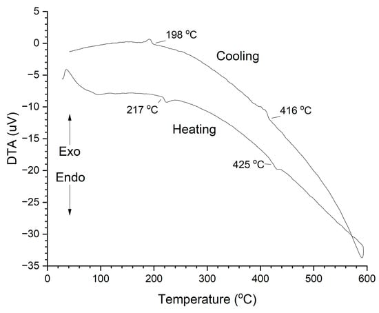
Figure 7.
DTA trace of a KNbO3 single crystal powder sample.
A Raman spectrum of a KNbO3 single crystal obtained at 25 °C is shown in Figure 8. The spectrum is typical of orthorhombic KNbO3 [1,51,52,53]. The sharp peak visible at ~200 cm−1 is a Fano resonance [54,55]. Raman spectra of the KNbO3 single crystal obtained at representative temperatures for each phase are shown in Figure 9. The spectra are typical for the different phases of KNbO3 [1,53]. Figure 10 shows a contour plot of normalised Raman intensity of the KNbO3 single crystal. Distinct changes in the contour plot appear at ~−20 °C, ~220 °C and ~440 °C. The normalised spectra obtained at different temperatures are shown in Figure 11. Not all of the spectra are shown to aid clarity. Significant changes in the spectra appear at −20 °C, 222~223 °C and 441 °C. According to group theory, the different phases of KNbO3 have the following optical modes [1,51]:
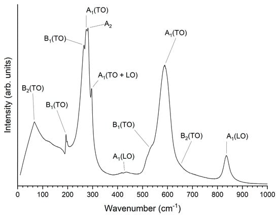
Figure 8.
Raman spectrum of a KNbO3 single crystal obtained at 25 °C.
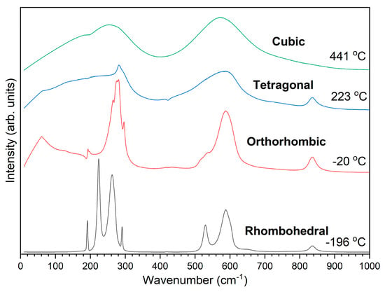
Figure 9.
Raman spectra of different phases of the KNbO3 single crystal.
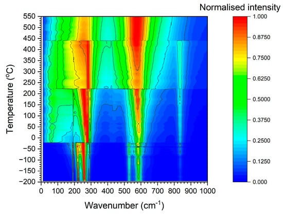
Figure 10.
Normalised Raman intensity contour plot of the KNbO3 single crystal.
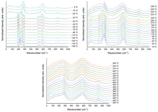
Figure 11.
Normalised Raman spectra of the KNbO3 single crystal obtained at different temperatures.
Rhombohedral: 3A1 ⊕ A2 ⊕ 4E;
Orthorhombic: 4A1 ⊕ A2 ⊕ 4B1 ⊕ 3B2;
Tetragonal: 3A1 ⊕ B1 ⊕ 4E;
Cubic: 3F1u ⊕ F2u.
The rhombohedral A2 mode and the cubic F2u mode are optically silent. Changes in the number and position of the modes are clearly seen in the Raman spectra at −20 °C, 222~223 °C and 441 °C, corresponding to the phase transitions. The disappearance of the A1(LO) mode at 441 °C is characteristic of the tetragonal–cubic phase transition in alkali niobates [1,56,57]. The cubic phase should not display any first-order Raman scattering as the unit cell is centrosymmetric [57]. The Raman scattering in the cubic phase indicates that the unit cell has a non-cubic distortion, which is due to displacements of the Nb ion in a <111> direction from its central position [58]. Rietveld and pair distribution function analysis of X-ray diffraction data found the local structure of all four phases of KNbO3 to be rhombohedral, with an off-centre shift of Nb in the NbO6 octahedra [4]. Nanometre-scale rhombohedral regions were observed in the cubic phase of KNbO3 by convergent beam electron diffraction [59]. The phase transition temperatures determined by Raman scattering match reasonably well with the orthorhombic–tetragonal and tetragonal–cubic phase transitions determined by DTA (Figure 7).
Plots of relative permittivity and loss tangent over the temperature range −200~176 °C are shown in Figure 12. A peak corresponding to the rhombohedral–orthorhombic phase transition can clearly be seen in the plots of relative permittivity at ~−20 °C on heating and ~−50 °C on cooling (Figure 12a,b). A thermal hysteresis of ~30 °C exists between heating and cooling plots, indicating the first-order nature of the phase transition. The phase transition is also visible in the plots of loss tangent on heating, although less so on cooling (Figure 12c,d). Thermal hysteresis is again present. The rhombohedral–orthorhombic phase transition temperature measured from the plots of relative permittivity and loss tangent agrees well with the temperature determined by Raman scattering. The phase transition temperature and large thermal hysteresis of the rhombohedral–orthorhombic phase transition are similar to those previously measured for KNbO3 single crystals [3].
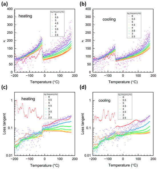
Figure 12.
Plots of (a,b) relative permittivity and (c,d) loss tangent versus temperature of a KNbO3 single crystal in the temperature range −200~176 °C.
Plots of relative permittivity and loss tangent over the temperature range 25~600 °C are shown in Figure 13. Peaks corresponding to the orthorhombic–tetragonal and tetragonal–cubic phase transitions can be seen at ~210 °C and ~430 °C, respectively, on heating (Figure 13a). There is an ~5 °C temperature hysteresis on heating and cooling. Peaks corresponding to the two phase transitions can also be seen in the plots of loss tangent (Figure 13c,d). Temperature hysteresis is more pronounced than in the relative permittivity plots, between 8~14 °C, being more pronounced for the orthorhombic–tetragonal phase transition than the tetragonal–cubic one. The orthorhombic–tetragonal and tetragonal–cubic phase transition temperatures are 5~10 °C lower than the corresponding temperatures determined by DTA and ~10 °C lower than the corresponding temperatures determined by Raman scattering. The orthorhombic–tetragonal and tetragonal–cubic phase transition temperatures measured by plots of relative permittivity and loss tangent are similar to those previously measured for KNbO3 single crystals, although the thermal hysteresis is less pronounced [3].
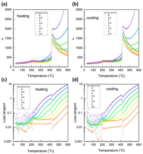
Figure 13.
Plots of (a,b) relative permittivity and (c,d) loss tangent versus temperature of a KNbO3 single crystal in the temperature range 25~600 °C.
Figure 14 shows plots of the inverse of relative permittivity versus temperature in the vicinity of the tetragonal-cubic phase transition i.e., the Curie Temperature Tc. The inverse relative permittivity shows a sharp decrease at Tc, which is characteristic of a first-order phase transition [60,61]. The decrease in inverse relative permittivity at Tc is more pronounced for the heating curve than for the cooling curve.
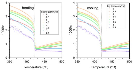
Figure 14.
Plots of inverse relative permittivity versus temperature of a KNbO3 single crystal in the temperature range 350~500 °C. The dashed lines are a guide to the eye.
3. Discussion
A suitable flux material should possess the following characteristics [36,44]: it should have a high solubility for the solute; the solute’s solubility in the flux should change noticeably with temperature; the flux should not form a solid solution or a compound with the solute; the flux should have a low melting point; the flux should have low volatility and viscosity at growth temperatures; the flux should not corrode the crucible; the flux should be fairly easy to separate from the grown single crystals; the flux should be non-toxic. From the phase diagram, it can be seen that KBO2 satisfies the first four requirements [40,41,42]. A solidified condensed phase often appears on the outside wall of the Pt crucible, implying that volatility of the flux may be a problem. KBO2 is soluble in water and so separation of the grown single crystals from the solidified flux is fairly easy, although some flux remains on the edges of the single crystals even after cleaning. KBO2 does not appear to corrode the Pt crucible and the crucible can be cleaned by soaking in warm 35% HCl for several days. Borates are toxic on ingestion, and KBO2 is suspected of damaging fertility or unborn children, so precautions should be taken when handling this material. Due to its small ionic radius, B is not expected to have considerable solid solubility in KNbO3 [36]. The first single crystal sample has a low B concentration, but the second crystal sample has a higher B concentration than expected. Comparing ionic radii and charge (K+ [coordination number of 12] = 0.164 nm, Nb5+ [coordination number of 6] = 0.064 nm, B3+ [coordination number of 6] = 0.027 nm [62]), B is expected to substitute for Nb in the KNbO3 crystal lattice. This is the case in the first sample, but in the second sample, B appears to substitute for both Nb and K.
According to Wenshan et al., the blue colour that sometimes appears in grown KNbO3 single crystals is caused by anti-site defects, which are charge compensated by oxygen vacancies to form colour centers [32]. No anti-site defects were visible in the HAADF-STEM image in Figure 6a, indicating that the bulk of the single crystal does not contain this defect. Indeed, the bulk of the single crystals is white, although the edges are blue (Figure 2), possibly containing this defect. Wenshan et al. [32] considered that the anti-site defects form when too much excess K2CO3 is used as a flux. It may be possible to reduce the blue colour by optimising the growth schedule or the amount of KBO2 flux. Varnhorst et al., based on their light scattering studies, considered the scattering to be caused by irregularities in the crystal lattice 60 nm in size [35]. Changes in the domain structure or size between the bulk and edges of the single crystals could affect the degree of light scattering and hence the colour.
4. Materials and Methods
KNbO3 powder was prepared by solid-state reaction, using K2CO3 (Daejung, 99.5%) and Nb2O5 (Daejung, 99.9%) as starting materials. All starting materials were dried in an oven at 250 °C for 5 h to remove absorbed water and then weighed based on the stoichiometric formula. K2CO3 and Nb2O5 starting materials were ball milled in a conventional ball mill (BML-2 ball mill, Daihan, Republic of Korea) with ZrO2 balls using high purity ethanol (Daejung, 99.9%) continuously for 24 h in a polypropylene jar with a rotation speed of 200 rpm. After ball milling, most of the ethanol was evaporated from the slurry using a hotplate/magnetic stirrer, then the slurry was completely dried in an oven at 70 °C overnight. The dried slurry was crushed and ground in an agate mortar and pestle and passed through a 180 µm sieve to remove agglomerates, followed by calcination at 850 °C for 5 h in air in an alumina crucible with a lid. The phase purity of the calcined powder was analysed by X-ray diffraction (XRD, X’Pert PRO, PANalytical, Almelo, the Netherlands) in Bragg–Brentano geometry using CuKα radiation with a scan range of 20–80°2θ, a step size of 0.026° and a scan speed of 3°/min. The calcined KNbO3 was re-mixed with K2CO3 and K2B4O7·4H2O (Acros, 99.5%) to obtain the composition of 75 mol % KNbO3 25 mol % KBO2. KBO2 is the product of the reaction:
K2CO3 + K2B4O7·4H2O → 4KBO2 + ↑4H2O (g) + ↑4CO2 (g)
The KNbO3 and K2CO3 powders were dried at 250 °C for 5 h before weighing and mixing. The K2B4O7·4H2O was not dried. The weight loss of H2O on heating was measured using differential thermogravimetry and compensated for when weighing out K2B4O7·4H2O. The materials were ball milled as before and calcined at 700 °C for 5 h to obtain KNbO3 with KBO2 as flux.
A schematic diagram of the single crystal growth process is shown in Figure 15. The KNbO3 + KBO2 batch was placed in a platinum crucible with a lid and put in an alumina crucible with a lid. The lid of the alumina crucible was sealed with alumina cement (Ceramabond 503, Aremco, Valley Cottage, NY) to reduce potassium evaporation. The cement was fired according to the manufacturer’s instructions. Single crystals of KNbO3 were grown according to the following heat-treatment schedule: heat from room temperature to 1060 °C at a rate of 5 °C/min and hold at 1060 °C for 5 h; cool from 1060 °C to 860 °C at a rate of 1 °C/h, then hold at 860 °C for 10 min; finally, cool from 860 °C to 25 °C at 1 °C/min. The single crystals were removed from the solidified flux by placing the Pt crucible in boiling water for 1 day to soften the flux. After removal, single crystals were placed in hot 1 N HNO3 and hot 10% HCl to remove any remaining flux.
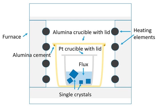
Figure 15.
Schematic diagram of the single crystal growth process.
For analysis, samples were separated from or cut out of the single crystals. The crystals for bulk XRD and single crystal XRD were separated from single crystal 2 in Figure 2b. The sample for TEM was obtained from single crystal 2 in Figure 2b. Samples for powder XRD, EPMA, DTA, Raman scattering and electrical property measurements were obtained from single crystals 1 or 3 in Figure 2b. The structure of the grown single crystals was analysed by XRD (X’Pert PRO, PANalytical, Almelo, The Netherlands) in Bragg–Brentano geometry using CuKα radiation with a scan range of 20–80°2θ, a step size of 0.026° and a scan speed of 3°/min. Both bulk and powdered samples were studied. Pattern smoothing and analysis was carried out using Match! version 3.10 (Crystal Impact, Bonn, Germany) with the Crystallography Open Database. Single crystal XRD was carried out using a Bruker APEX-II CCD-based diffractometer (Bruker AXS GmbH, Karlsruhe, Germany) with graphite-monochromated MoKα radiation (λ = 0.71073 Å). The hemisphere of the reflection data was collected as ω scan frames at 0.5°/frame and an exposure time of 5 s/frame. The cell parameters were determined and refined using the APEX2 program [63]. The data were corrected for Lorentz and polarisation effects and an empirical absorption correction was applied using the SADABS program [64]. The compound structures were solved by direct methods and refined by full matrix least squares using the SHELXTL program package [65] and Olex2 [66] with anisotropic thermal parameters for all non-hydrogen atoms. COD 3000498 contains the supplementary crystallographic data for this paper. These data can be obtained free of charge via http://www.crystallography.net/cod/search.html (accessed on 25 May 2024).
Electron probe microanalysis (EPMA, JEOL JXA-8530F PLUS, Tokyo, Japan) was carried out on two single crystal samples to determine their chemical composition. Samples were polished to a 1 μm finish using diamond paste. Wavelength-dispersive spectroscopy analysis was carried out on carbon-coated samples using an accelerating voltage of 15 kV. KNbO3, B (pure metal) and Al2O3 were used as standards. The first sample was analysed for K, Nb and B. The second sample was additionally analysed for Al to check if any Al contamination had occurred during processing.
Scanning transmission electron microscopy (STEM) was performed using an ARM 200CF microscope (JEOL, Tokyo, Japan) and Spectra 300 microscope (Thermo Fisher Scientific) equipped with Merlin and EMPAD pixelated detectors, respectively. The acceleration voltage was 200 kV for both microscopes. Samples for STEM were prepared by milling with a Ga+-source focused ion beam Helios Nanolab 650 HP (Thermo Fisher Scientific, Waltham, MA, USA).
For differential thermal analysis (DTA, DTG-60H, Shimadzu, Kyoto, Japan), a powder sample was analysed in air (flow rate of 50 mL/min) on heating and cooling in the temperature range from room temperature to 600 °C with heating and cooling rates of 10 °C/min.
For Raman scattering analysis, a single crystal sample was polished to a #2000 SiC finish, annealed for 1 h at 600 °C to remove polishing strains and cooled at a rate of 1 °C/min. Raman spectra were measured on heating from −196 °C to 550 °C using a heating stage (THMS600, Linkam, Tadworth, United Kingdom) in the wavenumber range from 10 to 1000 cm−1. The spectral resolution of the system was 1~2 cm−1. The diameter of the laser beam on the single crystal surface was 1~2 µm and the laser wavelength was 532 nm. Spectra were obtained at ~10 °C intervals except for regions around the expected phase transition temperatures, where the interval was reduced to ≤5 °C. All spectra were corrected by the Bose–Einstein factor [67].
For the impedance spectroscopy measurements, a single crystal sample was parallel polished on both major faces with SiC paper up to grade #4000 and Ag paste electrodes (16032 PELCO, Ted Pella, Redding, CA, USA) were applied. The thickness of the sample was 0.1032 cm and the electrode area was 0.063 cm2. Measurements were carried out over two temperature ranges. For the low-temperature range measurements, the sample was loaded in a cryostat (CCS-400/200, Janis, Woburn, MA, USA). Dielectric constant, loss tangent and conductivity were measured on heating and cooling in vacuum in the temperature range between −200 °C and 176 °C with heating and cooling rates of 1 °C/min by an impedance analyser (HP4284A, Hewlett-Packard, Kobe, Japan). For high-temperature measurements, the sample was loaded in a heating stage (TS1500, Linkam, Tadworth, UK). Dielectric constant, loss tangent and conductivity were measured on heating and cooling in N2 atmosphere in the temperature range between room temperature and 600 °C with heating and cooling rates of 1 °C/min by an impedance analyser (HP4284A, Hewlett-Packard, Kobe, Japan).
5. Conclusions
Single crystals of KNbO3 were grown by the flux method using KBO2 as a flux. Single crystals up to 15 mm in size could be grown. X-ray diffraction analysis revealed the room temperature phase to be orthorhombic with Cmm2 space group. Transmission electron microscopy analysis showed the existence of ferroelastic domains aligned on (110)pc crystallographic planes. anti-site defects could not be detected in the bulk of the crystals by STEM-HAADF, although they may be present at the edges of the crystals as shown by their blue colour. Raman scattering, differential thermal analysis and dielectric property measurements showed the existence of rhombohedral–orthorhombic, orthorhombic–tetragonal and tetragonal–cubic phase transitions at temperatures close to those in the literature.
Author Contributions
Conceptualisation, J.G.F.; data curation, T.T.D., J.G.F., H.T.T. and S.B.J.; formal analysis, T.T.D., J.G.F., H.T.T., J.M., J.L., A.B. and G.D.; funding acquisition, J.G.F., J.-S.L., A.B., G.D. and J.-H.K.; investigation, T.T.D., H.T.T., J.G., J.M., A.B., G.D. and S.B.J.; methodology, J.G.F. and J.-S.L.; project administration, J.G.F.; resources, J.G.F., J.-S.L., J.L., A.B., G.D. and J.-H.K.; supervision, J.G.F., J.-S.L., J.L. and J.-H.K.; validation, T.T.D. and H.T.T.; visualisation, T.T.D., J.G.F., A.B., G.D. and S.B.J.; writing—original draft, T.T.D. and J.G.F.; writing—review and editing, J.G.F., J.-S.L., J.G., A.B. and J.-H.K. All authors have read and agreed to the published version of the manuscript.
Funding
This work was supported by a National Research Foundation of Korea (NRF) grant funded by the Korean government (MSIT) (No. 2021R1F1A1046778). Jong-Sook Lee was supported by a National Research Foundation of Korea (NRF) grant funded by the Ministry of Science and ICT (MSIT) (Grant No. NRF-2018R1A5A1025224). Junseong Lee acknowledges financial support by the ‘Regional Innovation Strategy (RIS)’ through the National Research Foundation of Korea (NRF), funded by the Ministry of Education (MOE) (2021RIS-002). Jae-Hyeon Ko was supported by a National Research Foundation of Korea (NRF) grant funded by the Ministry of Science and ICT (MSIT) (grant no. 2020R1A2C101083111). Andreja Benčan and Goran Dražić were supported by the Slovenian Research and Innovation Agency (research project J7-4637).
Data Availability Statement
The data presented in this study are available on request from the corresponding author.
Acknowledgments
The authors would like to thank Jin-Hui Park (Center for Development of Fine Chemicals, Chonnam National University) for operating the DTA, Kyeong-Kap Jeong and Jung-Yeol Park (Centre for Research Facilities, Chonnam National University) for operating the XRD and EPMA, respectively. A.B and G.D. would like to thank Daniel Stroppa (DSTL GmbH) for his assistance with acquiring the iDPC and EDXS data and Maja Koblar (Jožef Stefan Institute) for preparing the STEM samples. J.G. would like to thank Kiran Andleeb for assistance with experiments.
Conflicts of Interest
The authors declare no conflicts of interest. The funders had no role in the design of the study; in the collection, analyses or interpretation of data; in the writing of the manuscript; or in the decision to publish the results.
References
- Baier-Saip, J.A.; Ramos-Moor, E.; Cabrera, A.L. Raman study of phase transitions in KNbO3. Solid State Commun. 2005, 135, 367–372. [Google Scholar] [CrossRef]
- Wood, E.A. Polymorphism in Potassium Niobate, Sodium Niobate, and other ABO3 Compounds. Acta Crystallogr. 1951, 4, 353–362. [Google Scholar] [CrossRef]
- Shirane, G.; Danner, H.; Pavlovic, A.; Pepinsky, R. Phase Transitions in Ferroelectric KNbO3. Phys. Rev. 1954, 93, 672–673. [Google Scholar] [CrossRef]
- Yoneda, Y.; Ohara, K.; Nagata, H. Local structure and phase transitions of KNbO3. Jpn. J. Appl. Phy. 2018, 57, 11UB07. [Google Scholar] [CrossRef]
- Tennery, V.J.; Hang, K.W. Thermal and X-Ray Diffraction Studies of the NaNbO3–KNbO3 System. J. Appl. Phys. 1968, 39, 4749–4753. [Google Scholar] [CrossRef]
- Jaffe, B.; Cook, W.R.; Jaffe, H. Perovskite Niobates and Tantalates. In Piezoelectric Ceramics; Academic Press: London, UK, 1971; pp. 185–212. [Google Scholar]
- Rödel, J.; Jo, W.; Seifert, K.T.P.; Anton, E.M.; Granzow, T.; Damjanovic, D. Perspective on the Development of Lead-free Piezoceramics. J. Am. Ceram. Soc. 2009, 92, 1153–1177. [Google Scholar] [CrossRef]
- Wu, J.; Xiao, D.; Zhu, J. Potassium–Sodium Niobate Lead-Free Piezoelectric Materials: Past, Present, and Future of Phase Boundaries. Chem. Rev. 2015, 115, 2559–2595. [Google Scholar] [CrossRef] [PubMed]
- Kakimoto, K.-I.; Masuda, I.; Ohsato, H. Ferroelectric and Piezoelectric Properties of KNbO3 Ceramics Containing Small Amounts of LaFeO3. Jpn. J. Appl. Phy. 2003, 42 Pt 1, 6102–6105. [Google Scholar] [CrossRef]
- Kakimoto, K.-i.; Masuda, I.; Ohsato, H. Solid-Solution Structure and Piezoelectric Property of KNbO3 Ceramics Doped with Small Amounts of Elements. Jpn. J. Appl. Phy. 2004, 43, 6706–6710. [Google Scholar] [CrossRef]
- Masuda, I.; Kakimoto, K.-I.; Ohsato, H. Ferroelectric Property and Crystal Structure of KNbO3 Based Ceramics. J. Electroceram. 2004, 13, 555–559. [Google Scholar] [CrossRef]
- Birol, H.; Damjanovic, D.; Setter, N. Preparation and Characterization of KNbO3 Ceramics. J. Am. Ceram. Soc. 2005, 88, 1754–1759. [Google Scholar] [CrossRef]
- Kim, D.-H.; Joung, M.-R.; Seo, I.-T.; Hur, J.; Kim, J.-H.; Kim, B.-Y.; Lee, H.-J.; Nahm, S. Influence of sintering conditions on piezoelectric properties of KNbO3 ceramics. J. Eur. Ceram. Soc. 2014, 34, 4193–4200. [Google Scholar] [CrossRef]
- Park, J.; Kim, D.H.; Lee, T.G.; Cho, S.H.; Park, S.J.; Ryu, J.; Nahm, S. CuO-added KNbO3-BaZrO3 lead-free piezoelectric ceramics with low loss and large electric field-induced strain. J. Am. Ceram. Soc. 2017, 100, 2948–2957. [Google Scholar] [CrossRef]
- Kim, D.-H.; Joung, M.-R.; Seo, I.-T.; Hur, J.; Kim, J.-H.; Kim, B.-Y.; Lee, H.-J.; Nahm, S. Low-Temperature Sintering and Piezoelectric Properties of CuO-Added KNbO3 Ceramics. J. Am. Ceram. Soc. 2014, 97, 3897–3903. [Google Scholar] [CrossRef]
- Davis, M.; Klein, N.; Damjanovic, D.; Setter, N.; Gross, A.; Wesemann, V.; Vernay, S.; Rytz, D. Large and stable thickness coupling coefficients of [001]C-oriented KNbO3 and Li-modified (K,Na)NbO3 single crystals. Appl. Phys. Lett. 2007, 90, 062904. [Google Scholar] [CrossRef]
- Adachi, H.; Wakabayashi, K.; Nishio, M.; Ogawa, H.; Kamakura, T. Fabrication of Ultrasonic Transducers with KNbO3 Piezoelectric Single Crystal for Detecting Harmonic Signals. Jpn. J. Appl. Phy. 2001, 40, 5698. [Google Scholar] [CrossRef]
- Rouffaud, R.; Marchet, P.; Hladky-Hennion, A.C.; Bantignies, C.; Pham-Thi, M.; Levassort, F. Complete electroelastic set for the (YXt)-45° cut of a KNbO3 single crystal. J. Appl. Phys. 2014, 116, 194106. [Google Scholar] [CrossRef]
- Pollard, T.B.; Kenny, T.D.; Vetelino, J.F.; Da Cunha, M.P. Pure SH-SAW propagation, transduction and measurements on KNbO3. IEEE Trans. Ultrason. Ferroelectr. Freq. Control. 2006, 53, 199–208. [Google Scholar] [CrossRef] [PubMed]
- Nakamura, K.; Oshiki, M.; Kitazume, H. SH-mode SAW and its acousto-optic interaction in KNbO3. In Proceedings of the IEEE Ultrasonics Symposium Proceedings (Cat. No. 98CH36102), Sendai, Japan, 5–8 October 1998; Volume 2, pp. 1305–1308. [Google Scholar]
- Yamanouchi, K.; Wagatsuma, Y.; Odagawa, H.; Cho, Y. Single crystal growth of KNbO3 and application to surface acoustic wave devices. J. Eur. Ceram. Soc. 2001, 21, 2791–2795. [Google Scholar] [CrossRef]
- Uematsu, Y. Nonlinear Optical Properties of KNbO3 Single Crystal in the Orthorhombic Phase. Jpn. J. Appl. Phy. 1974, 13, 1362–1368. [Google Scholar] [CrossRef]
- Fluck, D.; Gunter, P. Second-harmonic generation in potassium niobate waveguides. IEEE J. Sel. Top. Quantum Electron. 2000, 6, 122–131. [Google Scholar] [CrossRef]
- Lee, K.J.; Yoon, C.S.; Rotermund, F. Phase Matching Characteristics of Second-Harmonic Generation in Periodic 90°-Domain Structures of KNbO3. Jpn. J. Appl. Phy. 2007, 46, 7317. [Google Scholar] [CrossRef]
- Beckers, L.; Buchal, C.; Fluck, D.; Pliska, T.; Günter, P. Potassium niobate waveguides: He+ implantation in bulk single crystals and pulsed laser deposition of thin films. Mater. Sci. Eng. A 1998, 253, 292–295. [Google Scholar] [CrossRef]
- Irle, E.; Blachnik, R.; Gather, B. The phase diagrams of Na2O and K2O with Nb2O5 and the ternary system Nb2O5-Na2O-Yb2O3. Thermochim. Acta 1991, 179, 157–169. [Google Scholar] [CrossRef]
- Kudo, K.; Kakiuchi, K.; Mizutani, K.; Hoshikawa, K.; Fukami, T. Growth and Characterization of KNbO3 Single Crystal by Vertical Bridgman Method. Ferroelectrics 2005, 323, 157–164. [Google Scholar] [CrossRef]
- Ilangovan, R.; Balakumar, S.; Subramanian, C. Growth and characterisation of KNbO2 single crystals. Mater. Sci. Technol. 1999, 15, 132–136. [Google Scholar] [CrossRef]
- Xing, W.; Looser, H.; Wüest, H.; Arend, H. Progress in KNbO3 crystal growth. J. Cryst. Growth 1986, 78, 431–437. [Google Scholar] [CrossRef]
- Flückiger, U.; Arend, H. On the preparation of pure, doped and reduced KNbO3 single crystals. J. Cryst. Growth 1978, 43, 406–416. [Google Scholar] [CrossRef]
- Durugkar, P.D.; Katpatal, A.G. Growth and characterization of pure, and doped crystals of potassium niobate. J. Cryst. Growth 1996, 162, 161–166. [Google Scholar] [CrossRef]
- Wenshan, W.; Qun, Z.; Zhaohua, G. Investigation of the colour of KNbO3 single crystals grown by the radio-frequency heating Czochralski technique. J. Cryst. Growth 1987, 83, 62–68. [Google Scholar] [CrossRef]
- Takagi, T.; Fujii, T.; Sakabe, Y. Growth and characterization of KNbO3 by vertical Bridgman method. J. Cryst. Growth 2003, 259, 296–301. [Google Scholar] [CrossRef]
- Jiao, X.; Liu, T.; Lu, Y.; Li, Q.; Guo, R.; Wang, X.; Xu, X. Optical Properties of the Oxygen Vacancy in KNbO3 Crystal. J. Electron. Mater. 2020, 49, 2137–2143. [Google Scholar] [CrossRef]
- Varnhorst, T.; Schirmer, O.F.; Hesse, H. Blue coloration of KNbO3 caused by scattering. J. Cryst. Growth 1991, 108, 429–432. [Google Scholar] [CrossRef]
- Tachibana, M. Beginner’s Guide to Flux Crystal Growth; Springer: Tokyo, Japan, 2017. [Google Scholar]
- Bugaris, D.E.; Zur Loye, H.-C. Materials Discovery by Flux Crystal Growth: Quaternary and Higher Order Oxides. Angew. Chem. Int. Ed. 2012, 51, 3780–3811. [Google Scholar] [CrossRef] [PubMed]
- Watanabe, T.; Yabuta, H.; Ueda, M.; Watanabe, M.; Suzuki, T.; Miura, K.; Ito, N.; Kumada, N. Growth of (1-x)NaNbO3–xBaTiO3 Single Crystals by Slow-Cooling and Flux Methods. Jpn. J. Appl. Phy. 2013, 52, 09KC02. [Google Scholar] [CrossRef]
- Dec, J. Real domain structure in orthorhombic phase of NaNbO3 crystals. Cryst. Res. Technol. 1983, 18, 195–204. [Google Scholar] [CrossRef]
- Rudkovskaya, L.M.; Smotrakov, V.G. Thermogravimetric investigation of the KNbO3-KBO2 system. Inorg. Mater. 1982, 18, 911–912. [Google Scholar]
- Smotrakov, V.G.; Raevskij, I.P.; Rudkovskaya, L.M. Potassium metaniobate preparation in K2CO3–Nb2O5, K2CO3–Nb2O5–B2O3 system. Russ. J. Inorg. Chem. 1982, 27, 1875–1877. [Google Scholar]
- Smotrakov, V.G.; Raevskii, I.P.; Rudkovskaya, L.M. Fig. 09401-System KNbO3-KBO2. In ACerS-NIST Phase Equilibria Diagrams Version 3.3.0; Roth, R.S., Ed.; The American Ceramic Society: Westerville, OH, USA, 2010. [Google Scholar]
- Tian, H.; Hu, C.; Meng, X.; Tan, P.; Zhou, Z.; Li, J.; Yang, B. Top-Seeded Solution Growth and Properties of K1–xNaxNbO3 Crystals. Cryst. Growth Des. 2015, 15, 1180–1185. [Google Scholar] [CrossRef]
- Koruza, J.; Liu, H.; Höfling, M.; Zhang, M.-H.; Veber, P. (K,Na)NbO3-based piezoelectric single crystals: Growth methods, properties, and applications. J. Mater. Res. 2020, 35, 990–1016. [Google Scholar] [CrossRef]
- Lee, M. X-ray Diffraction for Materials Research: From Fundamentals to Applications; Apple Academic Press Inc.: Oakville, ON, Canada, 2016; pp. 182–223. [Google Scholar]
- Iamsasri, T.; Tutuncu, G.; Uthaisar, C.; Pojprapai, S.; Jones, J.L. Analysis methods for characterizing ferroelectric/ferroelastic domain reorientation in orthorhombic perovskite materials and application to Li-doped Na0.5K0.5NbO3. J. Mater. Sci. 2013, 48, 6905–6910. [Google Scholar] [CrossRef]
- Ochoa, D.A.; Esteves, G.; Iamsasri, T.; Rubio-Marcos, F.; Fernández, J.F.; García, J.E.; Jones, J.L. Extensive domain wall contribution to strain in a (K,Na)NbO3-based lead-free piezoceramics quantified from high energy X-ray diffraction. J. Eur. Ceram. Soc. 2016, 36, 2489–2494. [Google Scholar] [CrossRef]
- Deng, H.; Zhang, H.; Zhao, X.; Chen, C.; Wang, X.A.; Li, X.; Lin, D.; Ren, B.; Jiao, J.; Luo, H. Direct observation of monoclinic ferroelectric phase and domain switching process in (K0.25Na0.75)NbO3 single crystals. CrystEngComm 2015, 17, 2872–2877. [Google Scholar] [CrossRef]
- Hirohashi, J.; Yamada, K.; Kamio, H.; Uchida, M.; Shichijyo, S. Control of specific domain structure in KNbO3 single crystals by differential vector poling method. J. Appl. Phys. 2005, 98, 034107. [Google Scholar] [CrossRef]
- Skjærvø, S.L.; Høydalsvik, K.; Blichfeld, A.B.; Einarsrud, M.-A.; Grande, T. Thermal evolution of the crystal structure and phase transitions of KNbO3. R. Soc. Open Sci. 2018, 5, 180368. [Google Scholar] [CrossRef] [PubMed]
- Bhattacharjee, S.; Chattopadhyay, K.K. Laser-induced Fano interference subsumed by electron–phonon coupling in orthorhombic KNbO3 nano-bricks: An ab initio vibrational and Raman spectroscopic investigation. J. Raman Spectrosc. 2023, 54, 871–886. [Google Scholar] [CrossRef]
- Qi, W.; Xie, C.; Hushur, A.; Kojima, S. Pressure-induced successive phase transitions and Fano resonance engineering in lead-free piezoceramics KNbO3. Appl. Phys. Lett. 2023, 122, 232901. [Google Scholar] [CrossRef]
- Buixaderas, E.; Nuzhnyy, D.; Gregora, I.; Kamba, S.; Berta, M.; Malic, B.; Kosec, M. Lattice Dynamics and Phase Transitions in KNbO3 and K0.5Na0.5NbO3 Ceramics. IEEE Trans. Ultrason. Ferroelectr. Freq. Control. 2009, 56, 1843–1849. [Google Scholar] [CrossRef] [PubMed]
- Kuzmany, H. Solid-State Spectroscopy; Springer: Berlin/Heidelberg, Germany, 2009. [Google Scholar]
- Połomska, M.; Hilczer, B.; Kosec, M.; Malič, B. Raman Scattering Studies of Lead Free (1-x)K0.5Na0.5NbO3-xSrTiO3 Relaxors. Ferroelectrics 2008, 369, 149–156. [Google Scholar] [CrossRef]
- Trodahl, H.J.; Klein, N.; Damjanovic, D.; Setter, N.; Ludbrook, B.; Rytz, D.; Kuball, M. Raman spectroscopy of (K,Na)NbO3 and (K,Na)1−xLixNbO3. Appl. Phys. Lett. 2008, 93, 262901. [Google Scholar] [CrossRef]
- Klein, N.; Hollenstein, E.; Damjanovic, D.; Trodahl, H.J.; Setter, N.; Kuball, M. A study of the phase diagram of (K,Na,Li)NbO3 determined by dielectric and piezoelectric measurements, and Raman spectroscopy. J. Appl. Phys. 2007, 102, 014112. [Google Scholar] [CrossRef]
- Kodre, A.; Tellier, J.; Arčon, I.; Malič, B.; Kosec, M. Extended x-ray absorption fine structure study of phase transitions in the piezoelectric perovskite K0.5Na0.5NbO3. J. Appl. Phys. 2009, 105, 113528. [Google Scholar] [CrossRef]
- Tsuda, K.; Tanaka, M. Nanometer-scale local structural study of the paraelectric cubic phase of KNbO3 by convergent-beam electron diffraction. Jpn. J. Appl. Phy. 2017, 56, 10PB09. [Google Scholar] [CrossRef]
- Fridkin, V.M. Ferroelectric Semiconductors; Consultants Bureau: New York, NY, USA, 1980. [Google Scholar]
- Lines, M.E.; Glass, A.M. Principles and Applications of Ferroelectrics and Related Materials; Oxford University Press: Oxford, UK, 2001. [Google Scholar]
- Shannon, R.D. Revised effective ionic radii and systematic studies of interatomic distances in halides and chalcogenides. Acta Crystallogr. A 1976, 32, 751–767. [Google Scholar] [CrossRef]
- Bruker-AXS. APEX2; Version 2014.11-0; Bruker-AXS: Madison, WI, USA, 2014. [Google Scholar]
- Krause, L.; Herbst-Irmer, R.; Sheldrick, G.M.; Stalke, D. Comparison of silver and molybdenum microfocus X-ray sources for single-crystal structure determination. J. Appl. Crystallogr. 2015, 48, 3–10. [Google Scholar] [CrossRef] [PubMed]
- Sheldrick, G. Crystal structure refinement with SHELXL. Acta Cryst. C 2015, 71, 3–8. [Google Scholar] [CrossRef]
- Dolomanov, O.V.; Bourhis, L.J.; Gildea, R.J.; Howard, J.A.K.; Puschmann, H. OLEX2: A complete structure solution, refinement and analysis program. J. Appl. Crystallogr. 2009, 42, 339–341. [Google Scholar] [CrossRef]
- Svitelskiy, O.; Toulouse, J.; Yong, G.; Ye, Z.G. Polarized Raman study of the phonon dynamics in Pb(Mg1/3Nb2/3)O3 crystal. Phys. Rev. B 2003, 68, 104107. [Google Scholar] [CrossRef]
Disclaimer/Publisher’s Note: The statements, opinions and data contained in all publications are solely those of the individual author(s) and contributor(s) and not of MDPI and/or the editor(s). MDPI and/or the editor(s) disclaim responsibility for any injury to people or property resulting from any ideas, methods, instructions or products referred to in the content. |
© 2024 by the authors. Licensee MDPI, Basel, Switzerland. This article is an open access article distributed under the terms and conditions of the Creative Commons Attribution (CC BY) license (https://creativecommons.org/licenses/by/4.0/).