Article

Facile Preparation of Flexible Lateral 2D MoS2 Nanosheets for Photoelectrochemical Hydrogen Generation and Optoelectronic Applications

by
Ahmed Adel A. Abdelazeez
1,
Amira Ben Gouider Trabelsi
2,*,
Fatemah. H. Alkallas
2,
Samira Elaissi
2 and
Mohamed Rabia
3,4
1
Nanoscale Science, University of North Carolina at Charlotte, Charlotte, NC 28223, USA
2
Department of Physics, College of Science, Princess Nourah Bint Abdulrahman University, P.O. Box 84428, Riyadh 11671, Saudi Arabia
3
Nanomaterials Science Research Laboratory, Chemistry Department, Faculty of Science, Beni-Suef University, Beni-Suef 62514, Egypt
4
Nanophotonics and Applications Lab, Physics Department, Faculty of Science, Beni-Suef University, Beni-Suef 62514, Egypt
*
Author to whom correspondence should be addressed.
Photonics 2022, 9(9), 638; https://doi.org/10.3390/photonics9090638
Submission received: 28 July 2022 / Revised: 29 August 2022 / Accepted: 30 August 2022 / Published: 5 September 2022
(This article belongs to the Topic Optical and Optoelectronic Materials and Applications)

Abstract

:
Two-dimensional (2D) materials have attracted significant attention with their high optical response due to their interesting and unique fundamental phenomena. A lateral 2D MoS2 nanosheets was prepared via a facile one-step electrophoretic deposition method on polyethylene terephthalate (PET)/ITO. These nanosheets have been used as photoelectrode materials for photoelectrochemical (PEC) hydrogen generation and optoelectronics. The chemical structure and morphology were confirmed using X-ray diffraction (XRD), energy-dispersive X-ray spectroscopy (EDX), Raman, scanning electron microscope (SEM), and transmission electron microscopy (TEM). The optical absorbance of the 2D MoS2 nanosheets extended to the UV, Vis, and near-IR regions with a bandgap value of 1.59 eV. The testing of the prepared photoelectrode material, PET/ITO/MoS2, was carried out through a three-electrode system, in which the current density (Jph) value represents the rate of H2 gas evaluated. The Jph enhanced under light illumination compared to the dark conditions with values of 0.4 to 0.98 mA·cm−2, respectively. The produced photocurrent at V = 0 V was 0.44 mA·cm−2. This confirms the great abilities of the PET/ITO/MoS2 photoelectrode in light detection and hydrogen generation with high photoresponsivity values. Soon, our team will work on the development of a prototype of this three-electrode cell to convert the water directly into H2 fuel gas that could be applied in houses and factories, or even in advanced technology such as spacecraft and airplane F-35s by providing H2 gas as a renewable energy source.

1. Introduction

Energy depletion and pollution are two critical issues causing widespread concern around the world. Every year, the excessive consumption of fossil fuels, as well as the emission of toxic and hazardous substances such as dyes, heavy metals, and pesticides, pose a severe threat to Earth’s health and human life. Solar-energy technology is widely considered one of the most promising and influential technologies. This is due to its strong ability in separating water during the production of clean fuel, H2, as well as the reduction in CO2 gas emissions and degradation of organic contaminations that helps to protect the environment [1,2,3].
In this regard, using a photoelectrochemical (PEC) photoelectrode to convert solar energy into electricity is a viable method. This electrode should have a strong light-matter interaction, high conversion, low cost, a broad spectral response, great carrier transportation, and an efficient electron-hole pair separation to develop a high-performance PEC electrode [4,5,6]. The morphology of the prepared materials is highly improved through enlarging the surface area and active sites. Thus, nanosheets, nanowires, and nanotubes are promising materials for energy applications [7,8]. The enhancement of the morphology causes enhancement of the bandgap, which becomes more suitable for light absorbance in the Vis region [8].
Many photoanode materials and their nanostructures have been studied so far to ameliorate their performance of light capture and absorption. Due to their great chemical stability, broad spectral response, acceptable bandgap, and cost-effectiveness, semiconductor materials such as TiO2, CuO, transition metal dichalcogenides (TMDs, such as MoS2, WSe2), and ZnO gain more attention than Pt in PEC solar-energy applications [9,10].
On the other hand, the charge separation is fundamental for the match at the p–n junction. Consequently, the acceptor/donor interface produced by corresponding to the active materials’ band alignment may improve the charge separation (exciton dissociation) and photocarrier transit within the active layer. This will ensure a better photoelectrochemical solar-energy performance.
Several studies have previously documented high-speed charge transfers between TMD layers, which can occur in a fraction of a second in the nanostructured area under illumination. This effect is most noticeable in TMD heterostructures with type-II band alignments. The interlayers moving charges between TMDs generate hot excitons, which are layer-separated electron-hole pairs with large amounts of energy. This is an intermediary state before reaching the tightly bound exciton states. Because the extra energy lowers the binding energy, a longer electron-hole pair distance emerges, which is easier to break into free charge carriers resulting in a greater photocurrent production.
TMDs are truly two-dimensional (2D) materials displaying high semiconducting characteristics with flexible properties [11]. TMDs with a thickness of few nm have efficient light-matter interactions. They have a high capacity to absorb up to 5–10% of incident sunlight, which is one order greater in magnitude than common solar absorbers like GaAs and Si [12]. TMDs are one of the most essential materials with high-performance and flexible optical absorbance due to their high optical advantages.
Molybdenum disulfide (MoS2) has advanced semiconducting properties and high applicability making it promising for numerous fields such as photonics, electronics, and optoelectronics [13,14]. Indeed, MoS2 owns a broad-spectrum response in the range from UV to near IR [15] due to its thickness-modulated optical energy gap. This opens the door for its application in the photovoltaic domain [16].
The 2D MoS2 nanosheets (monolayers or multilayers) are a semiconducting substrate with nanoscale or QDs structures that facilitate the transition from photoexcited to charge-separated states. Additionally, MoS2 NSs have better photosensitivity compared to thin QD films due to the fewer grain boundaries and faster charge transport in MoS2 NSs. The optical and electronic properties of MoS2 depend on the bandgap, the bulk MoS2 has a bandgap of 1.3 eV, and this value is increased (1.5 to 1.9 eV) by the formation of 2D MoS2, and this is a promising range of bandgap; thus, the 2D MoS2 has promising optical applications [17,18].
This concept has been successfully applied to photodetectors based on QD-graphene hybrid active layers [18,19], as well as epitaxial growth of QDs on TMDs NSs and their near-infrared photo response [19]. However, no hybrid materials of semiconducting QDs and TMD-layered materials are laterally connected. Furthermore, for hybrid photoelectrodes, synthesis conditions are critical. It would be extremely beneficial to use wet-chemical methods to generate low-cost, solution-processable, air-stable hybrids. The fabrication methods of these materials need sophisticated equipment to provide the required vacuum and temperature conditions for film preparation [20,21]. Moreover, 2D MoS2 can be prepared using the mechanical exfoliation method but the prepared material particles are not uniform in morphology [19]. In addition, chemical or physical vapor deposition can be used for the 2D MoS2 preparation, but these methods are high cost and produce a low amount of MoS2 [20]. Liquid-phase exfoliation can produce a good quantity of MoS2, but not all particles are 2D in morphology as this depends on the type of solvent used [21].
Electrophoretic deposition (EPD) has many advantages over other methods of preparing films from nanometers to a few micrometers of structures on substrates with various shapes because the deposition rate of this method is high, with a low suspension viscosity [22,23]; moreover, this method produces highly controlled 2D MoS2.
This reports on the synthesis of 2D MoS2 nanosheets film that is deposited on PET/ITO substrate via a facile one-step EPD method, and used as the photoelectrode materials for PEC hydrogen generation and optoelectronics through light detection. Since the successful 2D graphene growth in 2004 by Novoselov et al. [24] through a simple mechanical exfoliation technique, this method became commonly used for 2D-material synthesis. These are obtained via a simple mechanical exfoliation with adhesive tape from bulk material. Despite the simplicity of such an approach, the obtained films across the substrate surface remain small in size, which makes it a time-consuming process. Chemical vapor deposition (CVD) is an effective way to fabricate 2D materials, especially TMDs. CVD is promising for growing large films on a wide range of substrates. The high energy consumption is one of the cons of the CVD process. Yu et al. [2] prepared a wafer-scale MoS2 via the CVD technique; however, it is a huge challenge to optimize all the associated 2D-growth parameters. Thus, the CVD method is considered complicated for 2D-materials synthesis. Compared to mechanical exfoliation and CVD, liquid exfoliation is a cost-effective and promising technique for fabricating a high yield of 2D materials via sonication for an optimized period of time in an ice bath to prevent damage to the nanosheets due to the heat effects. Liquid exfoliation is performed by placing the bulk materials in a suitable solvent, which is in most cases an organic solvent [3,25]. Choosing the solvent is a critical step since solvents have diverse surface energy, and a range of solvents display similar surface energy. Electrophoretic deposition (EPD) is a cost-effective, versatile, and simple technique that can be used for a wide range of materials to obtain a high yield on the surface of any conductive substrate; in addition, it enables us to control the amount of deposited materials by optimizing the various deposition parameters like voltage, the suspension concentration, and the deposition time [4,5] The chemical structure is confirmed using numerous analytical tools such as SEM, TEM, XRD, and Raman. Moreover, the optical properties are determined, and the bandgap is calculated. The current-voltage relation is studied under dark and light conditions, in which the hydrogen generation behavior is confirmed under the water-splitting reaction with a determination of the current density in the light and dark; in addition, the photocurrent is determined at V = 0 V. This behavior confirms the optoelectronic applications through the high response under the light in comparison with the dark.

2. Experiments and Measurements

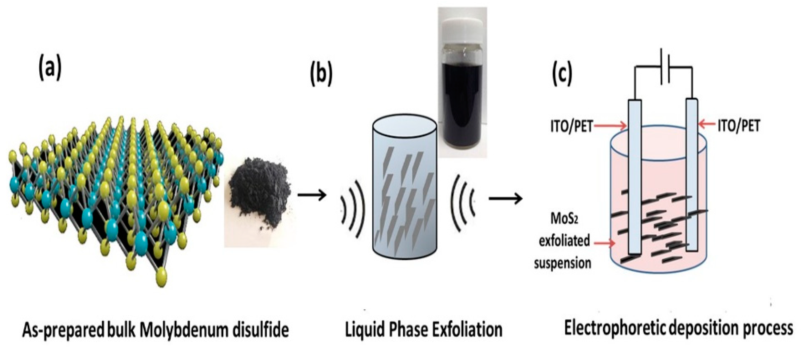
2.1. Synthesis of Bulk MoS2

For synthesized MoS2, 15 mg of Sodium molybdate (Na2MoO4) and 30 mg of acetic acid thioamide H4N2O2S were dissolved in 10 mL deionized water of and then stirred for 30 min. The homogeneous mixed solution was heated to 180 °C for 12 h under a pressure of 12 atm in a single-mode microwave reactor. MoS2 could be obtained after filtration following drying under a vacuum at 80 °C for 5 h.

2.2. Synthesis of 2D MoS2 Nanosheets Suspensions

The crystal structure of 2D MoS2 nanosheets is represented in Figure 1a. The typical liquid-phase exfoliation technique was used to obtain the 2D MoS2 nanosheets suspensions. Bulk MoS2 materials (3.5 g) were pulverized well using a mortar. Then, N-Methyl-2-pyrrolidone (NMP) was used as a suspension electrolyte for the dispersion of the pulverized materials at a concentration of 10 mg/mL. To obtain the exfoliated nanocrystals suspension, the mixture solution was sonicated for 10 h in an ice bath to stabilize the initial and final temperatures at 0 °C, with a horn probe sonic tip (VibraCell CVX, 750W, SONICS & MATERIALS, INC., Newtown, CT 06470, USA) at 60% amplitude, as shown in Figure 1b. The sonication was pulsed for 3 s on and 4 s off for completing the process smoothly and decreasing the solvent heating. Then, a uniform suspension of 2D MoS2 nanosheets could be obtained after centrifugation at 1000× g rpm for 60 min removing the larger particles. The suspensions of 2D MoS2 nanosheets were utilized as the precursor of film.

2.3. Preparation of 2D MoS2 Nanosheets Film

The EPD method is a simple, clean, and cost-effective method for preparing a film on the surface of any conductive substrate. A DC voltage of 7 V was applied between two electrodes of PET/ITO as a conducting substrate for the film deposition in the presence of the homogeneous MoS2 mixed suspension. The film was deposited on the PET/ITO substrate and then dried in a drying oven at 80 °C for 5 h.

2.4. Characterization and Measurement
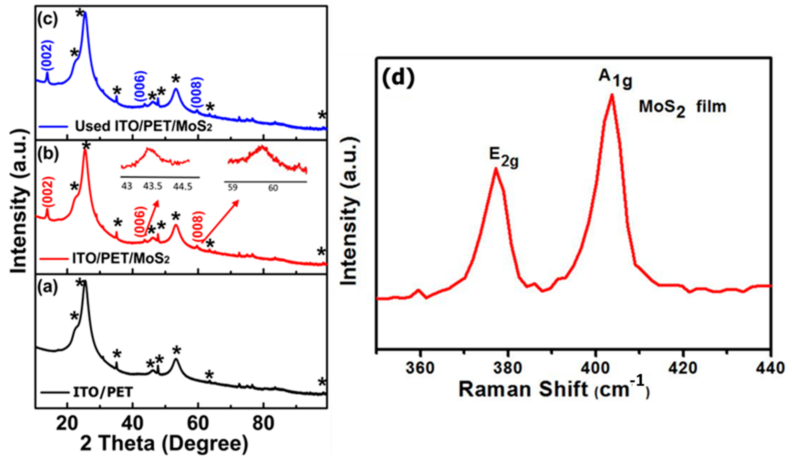
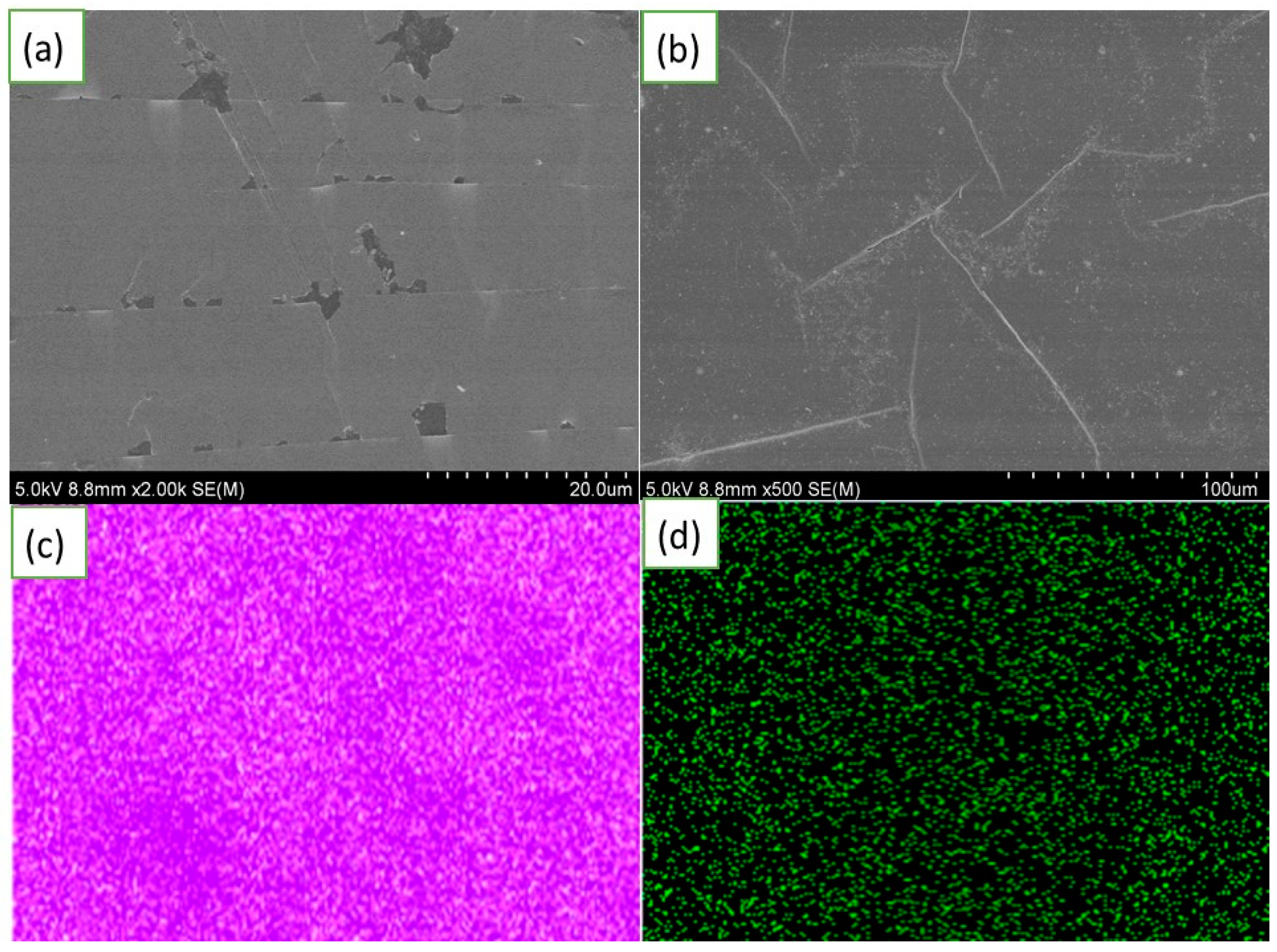
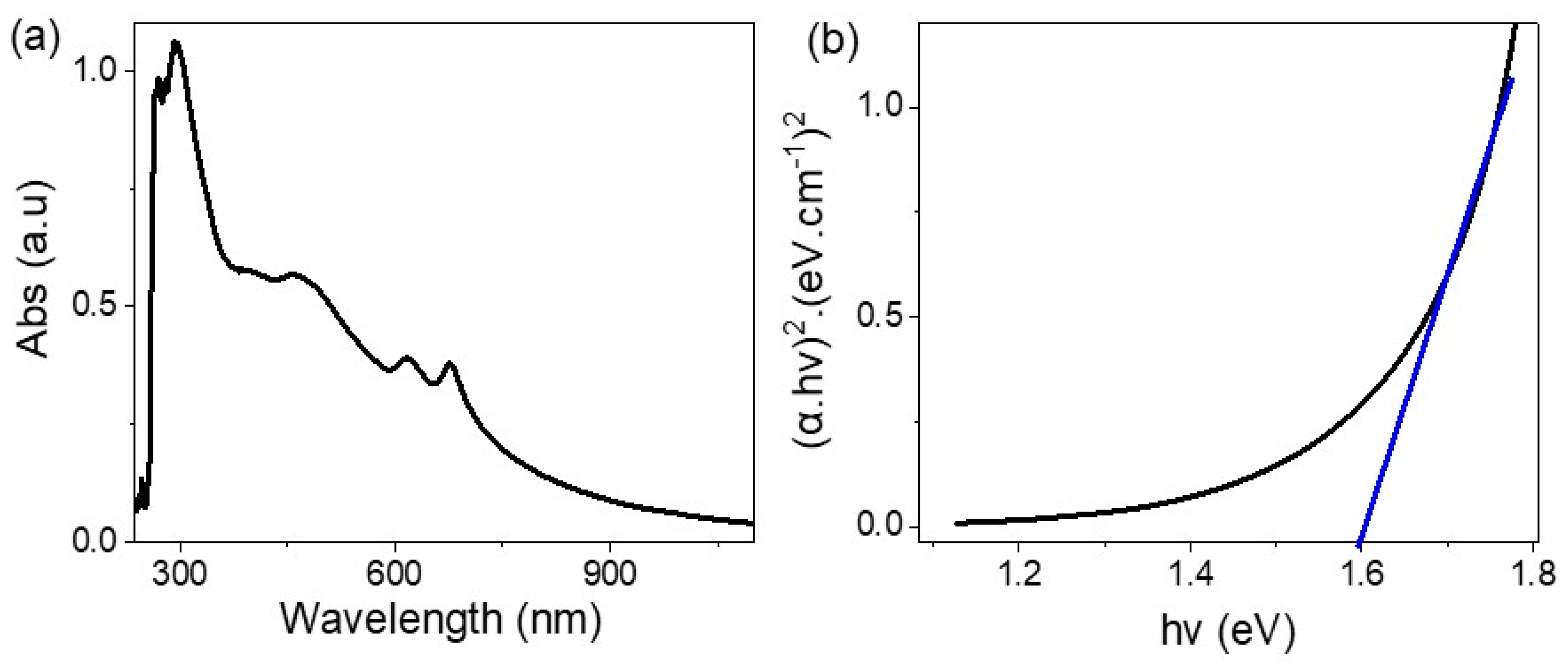
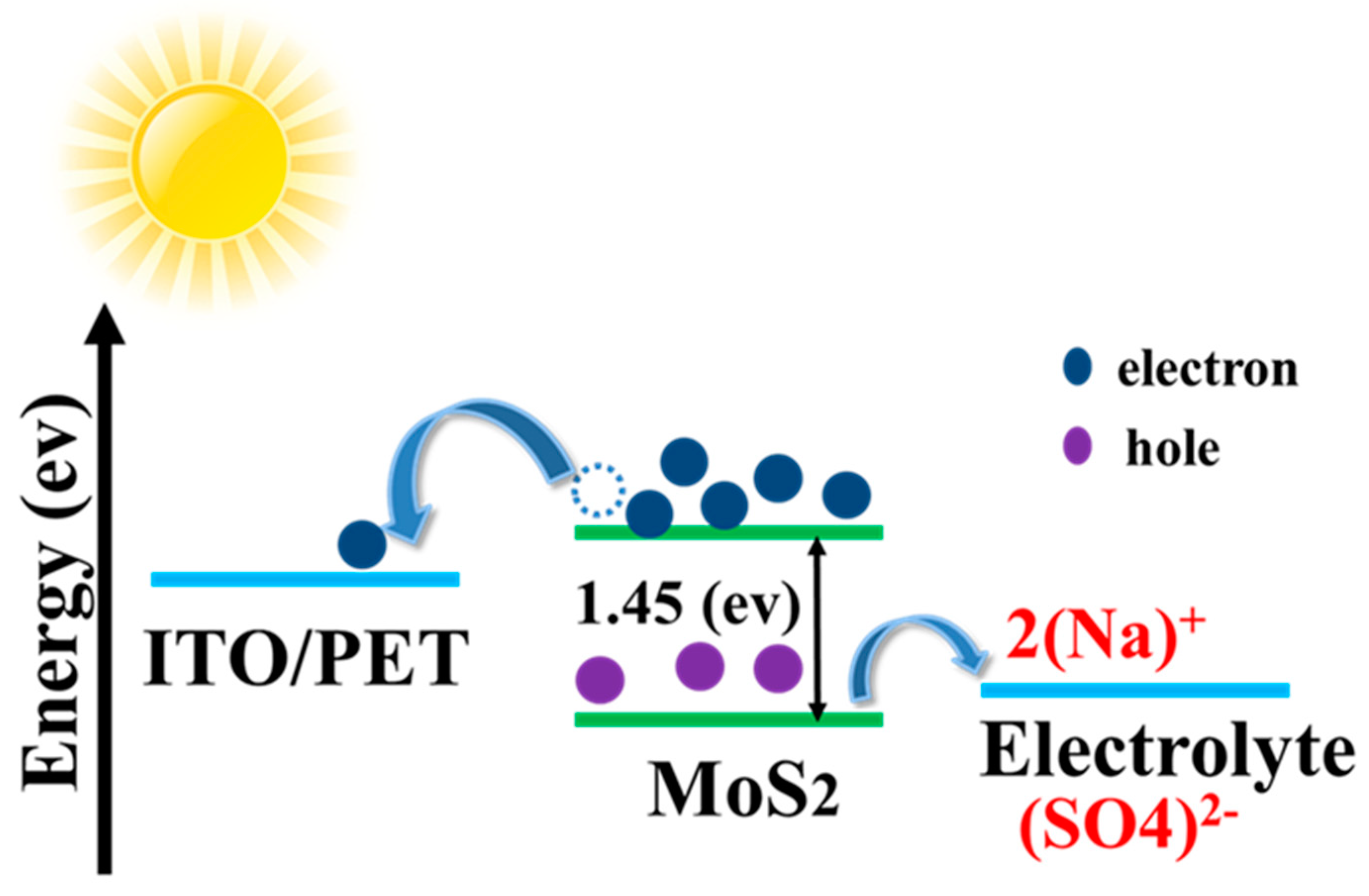
X-ray diffraction (XRD) and Raman were performed using Cu-Kα radiation (λ = 1.5406 Å) in the range from 2 theta 0 to 80° through on a Rigaku Smart Lab diffractometer and Raman spectrometer (HR Evolution, JY Horiba, Lille, France), respectively, for investigating the crystal structure. The micrograph was collected on an SEM microscope (SEM, Hitachi S-4800, Hitachi, Ltd., Tokyo, Japan) and transmission electron microscope (TEM, JEM-2010, JEOL, JEOL Ltd., Tokyo, Japan). The optical absorbance was carried out using a spectrophotometer (Perkin Elmer, PerkinElmer Ltd., Boston, MA, USA) in the spectral range from 250 to 1100 nm. PEC performance was evaluated using an electrochemical workstation (CHI 660E, Shanghai, China) via a standard three-electrode assembly. The prepared films were used as a photoelectrode material for PEC applications, where PET/ITO/MoS2 tests were performed in 0.5 M Na2SO4 (pH = 7) electrolyte via a standard three-electrode system. In this three-electrode system, the prepared film, Pt, and Ag/AgCl were applied as the working electrode (photoanode), the reference electrode, and the counter electrode, respectively. The illumination was carried out using a 300 W xenon lamp (PLS-SXE 300 C, Beijing Perfect Light Co., Ltd., Beijing, China).

3. Results

The XRD pattern of 2D MoS2 nanosheets film revealed a weak (002) peak for restacked MoS2, as shown in Figure 2a. The presence of (002) is attributed to the interplanar spacing between the nanosheets and its weakness refers to the highly exfoliated nature of the MoS2 nanosheet if it is compared with the as-prepared MoS2 bulk powder [26,27,28]. The (006) peak of 2H-MoS2 [28,29] demonstrates epitaxial growth along the out-of-plane direction [30]. The peaks, 002, 006, and 008, are small relative to the peaks of PET/ITO, so we added magnification, and the XRD device confirmed these peaks easily. The intensity values for the 002, 006 and 008 peaks are 88,497.5 (a.u.), 28,734.42 (a.u.) and 14,802 (a.u.), respectively.
We have determined the average grain size from the XRD data using the Scherrer Formula, given by the following equation:
Dp = (0.94 × λ)/(β × Cosθ)
where Dp = Average Crystallite size; β = Line broadening in radians; θ = Bragg angle; λ = X-ray wavelength.
The average size of particles calculated from the Scherrer formula is equal to 9.48 nm.
To further confirm the phase structure, Raman analysis was carried out on the 2D MoS2 nanosheets film using 532 nm laser excitation (see, Figure 2b). Raman spectra of MoS2 depict two prominent modes, E2g and A1g. The E2g mode shifts from 383.1 cm−1 to 379.3 cm−1 due to the in-plane vibration, while the A1g mode shifts from 408.2 cm−1 to 403.1 cm−1 due to the out-of-plane vibration [31,32]. These peaks are matched with the MoS2 analyses confirmed by Ho et al. [33], who prepared the material using pulsed laser deposition. Furthermore, it matched the MoS2 layers of different thicknesses earlier prepared by Lewandowska et al. [34], where it was demonstrated that the peak at 383 cm−1 moved to a low frequency, while the peak of 308 cm−1 moved to a higher frequency with rising MoS2 layer numbers.
The morphological properties of the prepared 2D MoS2 nanosheets films were investigated using the SEM analyses at different scales, as shown in Figure 3a,b. The lateral homogenous 2D MoS2 nanosheets are formed via a facile EPD method. The uniform and continuous coverage of the MoS2 grains is confirmed. Such film quality may affect the local density of states.
The EDX of the prepared MoS2 is shown in Figure 3c,d for the S and Mo particle mapping distribution, correspondingly. These figures show the uniform and continuous coverage of the MoS2 grains. Indeed, a high percentage of Mo and S atoms uniformly covering the entire PET/ITO films was observed.
The surface morphology and cross-section of the 2D MoS2 nanosheets are confirmed through the theoretical ImageJ program, as shown in Figure 4a. From this figure, the high homogenous distribution of MoS2 is illustrated. Such a homogenous distribution confirms the SEM and EDX results (Figure 3). Furthermore, the HRTEM image (Figure 4b,c) shows the 2D MoS2 nanosheets with an average sheet circumference of 80 nm. Although the HRTEM image (Figure 4d) indicated crystal lattice fringes of 0.27 nm that could be indexed to the (110) planes of MoS2 (see, Figure 2a). The high crystalline nature of MoS2 confirms the good optical properties of the prepared 2D MoS2 nanosheets and the promising photocatalytic applications. The surface roughness of the fabricated film was determined from AFM scans Figure S1.
The optical absorbance of the 2D MoS2 nanosheets is shown in Figure 5a. From this figure, four absorbance peaks were distinguished at 290, 467, 615, and 681 nm. The peak in the first three peaks is the result of the electron transfer inside the 2D MoS2 nanosheets. The peak at 681 nm, in the near-IR region, is associated with electron transfer and resonance inside the 2D MoS2 nanosheets. The broad optical absorbance for the spectrum that includes UV, Vis, and near-IR regions confirms the highly optical properties of 2D MoS2 nanosheets. This behavior is assigned to the highly crystalline structure of MoS2 as earlier demonstrated by the HRTEM analysis. The bandgap (Eg) was calculated from Tauc’s equations, Equations (2) and (3) [35,36,37], in which α , A, h, ν , and d symbols are the: absorption coefficient, absorbance, Planck’s constant, frequency, and density, respectively. Experimentally, the absorption coefficient (α) could be calculated from the equations below:
( α   h υ ) 2 = B   ( h υ E g   )
( α ) = 2.303   A / t
where (A) is absorbance and (t) is thickness of thin film, which is 0.63 µm in this case.
From Tauc’s equation, the bandgap value for 2D MoS2 nanosheets was 1.59 eV. So, the prepared MoS2 is highly qualified for photocatalytic applications, such as hydrogen generation and optoelectronics.
To investigate the PEC hydrogen generation and optoelectronic performance of the flexible PET/ITO/MoS2 photoelectrode, a three-electrode system was used to characterize their performance in 0.5 M Na2SO4 electrolytes. The prepared film was utilized as a photoelectrode, in which the Pt and Ag/AgCl are the reference electrode and the counter electrode, respectively. The illumination was carried out via a 300 W xenon lamp, but the measurements were carried out under 100 mW cm−2, as shown in Figure 6. From this figure, the effect of light illumination could be clearly distinguished where the Jph values increased from 0.4 to 0.98 mA·cm−2 in the dark and light, respectively. Such a photocurrent enhancement (Jph = 0.44 mA·cm−2) in light is related to high optical response to the light [38]. This behavior agrees with the optical absorption spectrum (see, Figure 5). Moreover, the good crystalline nature of these materials is shown by the HRTEM (see, Figure 4c).
The application of the prepared PET/ITO/MoS2 in PEC is related to the high photocurrent Jph value of 0.44 mA·cm−2 (Figure 6). This performance improvement of MoS2 film may come from the expansion of the spectral-response range and the enhancement of separating photoinduced electron-hole pairs [39]. The photocurrent tendency, as a function of visible light intensity, is a key parameter to evaluate photoelectrode performance [39,40,41,42,43]. From the Jph values, the PET/ITO/MoS2 is a promising electrode for water splitting and hydrogen generation applications.
The calculated hydrogen moles were 3.6 mmol/h for the prepared photoelectrode, PET/ITO/MoS2. This was determined through Equation (4) of Faraday’s law, which depends on the Jph and the change in time (dt), in addition to the Faraday constant (F). This H2 gas appeared as small bubbles. The comparisons with previous work of PET/ITO/MoS2 for hydrogen generation are mentioned in Table 1.
H 2 ( moles ) = 0 t J ph dt F · 1 / 2
The optoelectronic behavior appeared well through the high response of the electrode for light, where Jph increases with a great value in light in comparison with the dark. This process indicates the ability of the prepared photoelectrode for light capture and generation of electrons, which represents optoelectronic sensitivity. To further understand the charge transfer pathways in 2D MoS2 nanosheets film as a photocathode of PEC hydrogen generation and as an optoelectronic, a schematic diagram is presented in Figure 7. The 2D MoS2 nanosheets film absorbed visible light, and then photo-induced electrons (green bolus) and holes (yellow bolus) were generated in the conduction and valence band [44]. Then there was an electron transfer to the ITO, while the holes were transferred to the solution for additional water splitting and hydrogen generation reactions. The high optical properties of the MoS2 cause the absorbance of the light in a broad range of the optical zone regions. This results in high electron density in the conducting band (Figure 5), with many holes in the valency band that motivate the H2 evolution reaction. With increasing the water-splitting reaction and H2 evolution, the produced Jph values increase, in which Jph represents the rate of H2 reaction [39].
The effective generation of the hydrogen gas remained steady over our experimental measurement time which lasted for nearly 6 months. The calculated hydrogen moles were 3.6 mmol/h for the prepared photoelectrode, PET/ITO/MoS2. We were able to reuse the same electrode for several I-V measurements without deterioration. We added the XRD after using the catalyst, 2D MoS2 Nanosheets (Figure 2c); the XRD before and after the catalyst display almost the same behavior with the same peaks. This indicates the high stability and reproducibility of the catalyst.

4. Conclusions

A lateral 2D MoS2 nanosheet was prepared via an EPD method. SEM, EDX, and HRTEM confirmed the uniform morphology with a particle size of 60 nm. The XRD established the chemical structure for the prepared 2D MoS2. The band gap value was 1.59 eV, determined from the optical spectrum. The PET/ITO/MoS2 electrode is used for hydrogen generation via a xenon lamp as the light source from 0.5 M Na2SO4. The Jph values are 0.4 to 0.98 mA·cm−2 in the dark and light, respectively. Moreover, photocurrent is determined at V = 0 V, in which the Jph value is 0.44 mA·cm−2. The high response of the electrode under light indicates the optoelectronic behavior of the photoelectrode. The prepared electrode is very cheap and easy to synthesize using the low-cost technique. Soon, a prototype of this electrode will be fabricated and applied for hydrogen generation from wastewater.

Supplementary Materials

The following supporting information can be downloaded at: https://www.mdpi.com/article/10.3390/photonics9090638/s1, Figure S1: (a) AFM image and (b) the corresponding height profile.

Author Contributions

Conceptualization, A.A.A.A., A.B.G.T., F.H.A., S.E. and M.R. methodology, A.A.A.A., A.B.G.T., F.H.A., S.E. and M.R.; validation, A.A.A.A., A.B.G.T. and M.R.; formal analysis, A.A.A.A., A.B.G.T., F.H.A., S.E. and M.R. investigation, A.A.A.A., A.B.G.T., F.H.A., S.E. and M.R.; data curation, A.A.A.A., A.B.G.T., F.H.A., S.E. and M.R.; writing—original draft preparation, A.A.A.A., A.B.G.T., F.H.A., S.E. and M.R.; writing—review and editing, A.A.A.A., A.B.G.T., F.H.A., S.E. and M.R.; visualization, A.A.A.A., A.B.G.T., F.H.A., S.E. and M.R.; supervision, A.A.A.A., A.B.G.T., F.H.A., S.E. and M.R.; project administration, A.B.G.T. and F.H.A.; funding acquisition A.B.G.T. and F.H.A. All authors have read and agreed to the published version of the manuscript.

Funding

This research was funded by Princess Nourah bint Abdulrahman University Research Supporting Project number (PNURSP2022R223), Princess Nourah bint Abdulrahman University, Riyadh, Saudi Arabia.

Institutional Review Board Statement

Not applicable.

Informed Consent Statement

Not applicable.

Data Availability Statement

Not applicable.

Acknowledgments

The authors express their gratitude to Princess Nourah bint Abdulrahman University Researchers Supporting Project number (PNURSP2022R223), Princess Nourah bint Abdulrahman University, Riyadh, Saudi Arabia.

Conflicts of Interest

The authors declare no conflict of interest.

References

  1. Nishiyama, H.; Yamada, T.; Nakabayashi, M.; Maehara, Y.; Yamaguchi, M.; Kuromiya, Y.; Nagatsuma, Y.; Tokudome, H.; Akiyama, S.; Watanabe, T.; et al. Photocatalytic solar hydrogen production from water on a 100-m2 scale. Nature 2021, 598, 304–307. [Google Scholar] [CrossRef]
  2. Hisatomi, T.; Domen, K. Reaction systems for solar hydrogen production via water splitting with particulate semiconductor photocatalysts. Nat. Catal. 2019, 2, 387–399. [Google Scholar] [CrossRef]
  3. Takata, T.; Jiang, J.; Sakata, Y.; Nakabayashi, M.; Shibata, N.; Nandal, V.; Seki, K.; Hisatomi, T.; Domen, K. Photocatalytic water splitting with a quantum efficiency of almost unity. Nature 2020, 581, 411–414. [Google Scholar] [CrossRef]
  4. Avcu, E.; Bastan, F.E.; Abdullah, H.Z.; Rehman, M.A.U.; Avcu, Y.Y.; Boccaccini, A.R. Electrophoretic deposition of chitosan-based composite coatings for biomedical applications: A review. Prog. Mater. Sci. 2019, 103, 69–108. [Google Scholar] [CrossRef]
  5. Hernandez, Y.; Nicolosi, V.; Lotya, M.; Blighe, F.M.; Sun, Z.; De, S.; McGovern, I.T.; Holland, B.; Byrne, M.; Gun’Ko, Y.K.; et al. High-yield production of graphene by liquid-phase exfoliation of graphite. Nat. Nanotechnol. 2008, 3, 563–568. [Google Scholar] [CrossRef] [PubMed]
  6. Park, C.; Ounaies, Z.; Watson, K.A.; Crooks, R.E.; Smith, J., Jr.; Lowther, S.E.; Connell, J.W.; Siochi, E.J.; Harrison, J.S.; St Clair, T.L. Dispersion of single wall carbon nanotubes by in situ Dispersion of single wall carbon nanotubes by in situ polymerization under sonication. Chem. Phys. Lett. 2002, 364, 303–308. [Google Scholar] [CrossRef]
  7. Yu, Y.; Li, C.; Liu, Y.; Su, L.; Zhang, Y.; Cao, L. Controlled Scalable Synthesis of Uniform, High-Quality Monolayer and Few-layer MoS2 Films. Sci. Rep. 2013, 3, srep01866. [Google Scholar] [CrossRef] [PubMed]
  8. Novoselov, K.S.; Geim, A.K.; Morozov, S.V.; Jiang, D.; Zhang, Y.; Dubonos, S.V.; Grigorieva, I.V.; Firsov, A.A. Electric field effect in atomically thin carbon films. Science 2004, 306, 666–669. [Google Scholar] [CrossRef]
  9. Tilley, S.D. Recent Advances and Emerging Trends in Photo-Electrochemical Solar Energy Conversion. Adv. Energy Mater. 2019, 9, 1802877. [Google Scholar] [CrossRef]
  10. Masudy-Panah, S.; Eugene, Y.J.; Khiavi, N.D.; Katal, R.; Gong, X. Aluminum-incorporated p-CuO/n-ZnO photocathode coated with nanocrystal-engineered TiO2 protective layer for photoelectrochemical water splitting and hydrogen generation. J. Mater. Chem. A 2018, 6, 11951–11965. [Google Scholar] [CrossRef]
  11. Diez-Perez, I.; Li, Z.; Guo, S.; Madden, C.; Huang, H.; Che, Y.; Yang, X.; Zang, L.; Tao, N. Ambipolar transport in an electrochemically gated single-molecule field-effect transistor. ACS Nano 2012, 6, 7044–7052. [Google Scholar] [CrossRef] [PubMed]
  12. Akama, T.; Okita, W.; Nagai, R.; Li, C.; Kaneko, T.; Kato, T. Schottky solar cell using few-layered transition metal dichalcogenides toward large-scale fabrication of semitransparent and flexible power generator. Sci. Rep. 2017, 7, 11967. [Google Scholar] [CrossRef] [PubMed]
  13. Liu, H.; Luo, A.-P.; Wang, F.-Z.; Tang, R.; Liu, M.; Luo, Z.-C.; Xu, W.-C.; Zhao, C.-J.; Zhang, H. Femtosecond pulse erbium-doped fiber laser by a few-layer MoS2 saturable absorber. Opt. Lett. 2014, 39, 4591–4594. [Google Scholar] [CrossRef] [PubMed]
  14. Zhang, H.; Lu, S.B.; Zheng, J.; Du, J.; Wen, S.C.; Tang, D.Y.; Loh, K. Molybdenum disulfide (MoS2) as a broadband saturable absorber for ultra-fast photonics. Opt. Express 2014, 22, 7249–7260. [Google Scholar] [CrossRef] [PubMed]
  15. Hwang, D.K.; Lee, Y.T.; Lee, H.S.; Lee, Y.J.; Shokouh, S.H.H.; Kyhm, J.; Lee, J.; Kim, H.H.; Yoo, T.-H.; Nam, S.H.; et al. Ultrasensitive PbS quantum-dot-sensitized InGaZnO hybrid photoinverter for near-infrared detection and imaging with high photogain. NPG Asia Mater. 2016, 8, e233. [Google Scholar] [CrossRef]
  16. Wang, S.; Yu, H.; Zhang, H.; Wang, A.; Zhao, M.; Chen, Y.; Mei, L.; Wang, J. Broadband few-layer MoS2 saturable absorbers. Adv. Mater. 2014, 26, 3538–3544. [Google Scholar] [CrossRef]
  17. Li, Z.; Meng, X.; Zhang, Z. Recent development on MoS2-based photocatalysis: A review. J. Photochem. Photobiol. C Photochem. Rev. 2018, 35, 39–55. [Google Scholar] [CrossRef]
  18. Doustkhah, E.; Assadi, M.H.N.; Komaguchi, K.; Tsunoji, N.; Esmat, M.; Fukata, N.; Tomita, O.; Abe, R.; Ohtani, B.; Ide, Y. In situ Blue titania via band shape engineering for exceptional solar H2 production in rutile TiOAppl. Catal. B Environ. 2021, 297, 120380. [Google Scholar] [CrossRef]
  19. Song, I.; Park, C.; Choi, H.C. Synthesis and properties of molybdenum disulphide: From bulk to atomic layers. RSC Adv. 2015, 5, 7495–7514. [Google Scholar] [CrossRef]
  20. Coleman, J.N.; Lotya, M.; O’Neill, A.; Bergin, S.D.; King, P.J.; Khan, U.; Young, K.; Gaucher, A.; De, S.; Smith, R.J.; et al. Two-Dimensional Nanosheets Produced by Liquid Exfoliation of Layered Materials. Science 2011, 331, 568–571. [Google Scholar] [CrossRef] [Green Version]
  21. He, Z.; Que, W. Molybdenum disulfide nanomaterials: Structures, properties, synthesis and recent progress on hydrogen evolution reaction. Appl. Mater. Today 2016, 3, 23–56. [Google Scholar] [CrossRef]
  22. Besra, L.; Liu, M. A review on fundamentals and applications of electrophoretic deposition (EPD). Prog. Mater. Sci. 2007, 52, 1–61. [Google Scholar] [CrossRef]
  23. Corni, I.; Ryan, M.P.; Boccaccini, A.R. Electrophoretic deposition: From traditional ceramics to nanotechnology. J. Eur. Ceram. Soc. 2008, 28, 1353–1367. [Google Scholar] [CrossRef]
  24. Nikonovas, T.; Spessa, A.; Doerr, S.H.; Clay, G.D.; Mezbahuddin, S. Near-complete loss of fire-resistant primary tropical forest cover in Sumatra and Kalimantan. Commun. Earth Environ. 2020, 1, 65. [Google Scholar] [CrossRef]
  25. Pagliaro, M. Preparing for the future: Solar energy and bioeconomy in the United Arab Emirates. Energy Sci. Eng. 2019, 7, 1451–1457. [Google Scholar] [CrossRef]
  26. Zhang, B.; Wang, Z.; Peng, X.; Wang, Z.; Zhou, L.; Yin, Q. A Novel Route to Manufacture 2D Layer MoS2 and g-C3N4 by Atmospheric Plasma with Enhanced Visible-Light-Driven Photocatalysis. Nanomaterials 2019, 9, 1139. [Google Scholar] [CrossRef] [PubMed]
  27. Sun, Z.; Zhao, Q.; Zhang, G.; Li, Y.; Zhang, G.; Zhang, F.; Fan, X. Exfoliated MoS2 supported Au–Pd bimetallic nanoparticles with core–shell structures and superior peroxidase-like activities. RSC Adv. 2015, 5, 10352–10357. [Google Scholar] [CrossRef]
  28. De-Mello, G.B.; Smith, L.; Rowley-Neale, S.J.; Gruber, J.; Hutton, S.J.; Banks, C.E. Surfactant-exfoliated 2D molybdenum disulphide (2D-MoS2): The role of surfactant upon the hydrogen evolution reaction. RSC Adv. 2017, 7, 36208–36213. [Google Scholar] [CrossRef]
  29. Yue, X.; Yang, J.; Li, W.; Jing, Y.; Dong, L.; Zhang, Y.; Li, X. Electron Irradiation Induces the Conversion from 2H-WSe2 to 1T-WSe2 and Promotes the Performance of Electrocatalytic Hydrogen Evolution. ACS Sustain. Chem. Eng. 2022, 10, 2420–2428. [Google Scholar] [CrossRef]
  30. Sharma, U.; Karazhanov, S.; Jose, R.; Das, S. Plasmonic hot-electron assisted phase transformation in 2D-MoS2 for the hydrogen evolution reaction: Current status and future prospects. J. Mater. Chem. A 2022, 10, 8626–8655. [Google Scholar] [CrossRef]
  31. Saha, D.; Kruse, P. Editors’ choice—Review—Conductive forms of MoS2 and their applications in energy storage and conversion. J. Electrochem. Soc. 2020, 167, 126517. [Google Scholar] [CrossRef]
  32. Xia, Z.; Tao, Y.; Pan, Z.; Shen, X. Enhanced photocatalytic performance and stability of 1T MoS2 transformed from 2H MoS2 via Li intercalation. Results Phys. 2019, 12, 2218–2224. [Google Scholar] [CrossRef]
  33. Ho, Y.T.; Ma, C.H.; Luong, T.T.; Wei, L.L.; Yen, T.C.; Hsu, W.T.; Chang, W.H.; Chu, Y.C.; Tu, Y.Y.; Pande, K.P.; et al. Layered MoS2 grown on c-sapphire by pulsed laser deposition. Phys. Status Solidi (RRL)–Rapid Res. Lett. 2015, 9, 187–191. [Google Scholar] [CrossRef]
  34. Lewandowska, R. Number of layers of MoS2 determined using Raman Spectroscopy. Horiba Sci. 2014, 104, 109933. [Google Scholar]
  35. Baishya, K.; Ray, J.S.; Dutta, P.; Das, P.P.; Das, S.K. Graphene-mediated band gap engineering of WO3 nanoparticle and a relook at Tauc equation for band gap evaluation. Appl. Phys. A 2018, 124, 704. [Google Scholar] [CrossRef]
  36. Ingle, N.N.; Shirsat, S.; Sayyad, P.; Bodkhe, G.; Patil, H.; Deshmukh, M.; Mahadik, M.; Singh, F.; Shirsat, M. Influence of swift heavy ion irradiation on sensing properties of nickel-(NRs-Ni3HHTP2) metal-organic framework. J. Mater. Sci. Mater. Electron. 2021, 32, 18657–18668. [Google Scholar] [CrossRef]
  37. Abd-Elmageed, A.; Al-Hossainy, A.; Fawzy, E.; Almutlaq, N.; Eid, M.; Bourezgui, A.; Abdel-Hamid, S.; Elsharkawy, N.; Zwawi, M.; Abdel-Aziz, M.; et al. Synthesis, characterization and DFT molecular modeling of doped poly (para-nitroaniline-co-para-toluidine) thin film for optoelectronic devices applications. Opt. Mater. 2020, 99, 109593. [Google Scholar] [CrossRef]
  38. Abdelazeez, A.A.A.; El-Fatah, G.A.; Shaban, M.; Ahmed, A.M.; Rabia, M. ITO/Poly-3-Methylaniline/Au Electrode for Electrochemical Water Splitting and Dye Removal. ECS J. Solid State Sci. Technol. 2021, 10, 123009. [Google Scholar] [CrossRef]
  39. Elsayed, A.M.; Rabia, M.; Shaban, M.; Aly, A.H.; Ahmed, A.M. Preparation of hexagonal nanoporous Al2O3/TiO2/TiN as a novel photodetector with high efficiency. Sci. Rep. 2021, 11, 17572. [Google Scholar] [CrossRef]
  40. Rabia, M.; Mohamed, H.S.H.; Shaban, M.; Taha, S. Preparation of polyaniline/PbS core-shell nano/microcomposite and its application for photocatalytic H2 electrogeneration from H2O. Sci. Rep. 2018, 8, 1107. [Google Scholar] [CrossRef]
  41. Mohamed, S.; Zhao, H.; Romanus, H.; El-Hossary, F.; El-Kassem, M.A.; Awad, M.; Rabia, M.; Lei, Y. Optical, water splitting and wettability of titanium nitride/titanium oxynitride bilayer films for hydrogen generation and solar cells applications. Mater. Sci. Semicond. Process. 2020, 105, 104704. [Google Scholar] [CrossRef]
  42. Shaban, M.; Abukhadra, M.R.; Rabia, M.; Elkader, Y.A.; El-Halim, M.R.A. Investigation the adsorption properties of graphene oxide and polyaniline nano/micro structures for efficient removal of toxic Cr(VI) contaminants from aqueous solutions; kinetic and equilibrium studies. Rendiconti Lince Sci. Fis. E Nat. 2018, 29, 141–154. [Google Scholar] [CrossRef]
  43. Shaban, M.; Rabia, M.; Eldakrory, M.G.; Maree, R.M.; Ahmed, A.M. Efficient photoselectrochemical hydrogen production utilizing of APbI3 (A = Na, Cs, and Li) perovskites nanorods. Int. J. Energy Res. 2021, 45, 7436–7446. [Google Scholar] [CrossRef]
  44. Elsayed, A.M.; Shaban, M.; Aly, A.H.; Ahmed, A.M.; Rabia, M. Preparation and characterization of a high-efficiency photoelectric detector composed of hexagonal Al2O3/TiO2/TiN/Au nanoporous array. Mater. Sci. Semicond. Process. 2022, 139, 106348. [Google Scholar] [CrossRef]
  45. Yao, H.; Luo, S.; Duesberg, G.S.; Qi, X.; Lu, D.; Yue, C.; Zhong, J. Enhanced photoresponse of graphene oxide functionalised SnSe films. AIP Adv. 2018, 8, 075123. [Google Scholar] [CrossRef]
  46. Arulanantham, A.; Valanarasu, S.; Jeyadheepan, K.; Ganesh, V.; Shkir, M. Development of SnS (FTO/CdS/SnS) thin films by nebulizer spray pyrolysis (NSP) for solar cell applications. J. Mol. Struct. 2018, 1152, 137–144. [Google Scholar] [CrossRef]
  47. Tyona, M. Doped Zinc Oxide Nanostructures for Photovoltaic Solar Cells application. In Zinc Oxide Based Nano Materials and Devices; IntechOpen: London, UK, 2019. [Google Scholar]
  48. Patel, A.B.; Machhi, H.K.; Chauhan, P.; Narayan, S.; Dixit, V.; Soni, S.S.; Jha, P.K.; Solanki, G.K.; Patel, K.D.; Pathak, V.M. Electrophoretically deposited MoSe2/WSe2 heterojunction from ultrasonically exfoliated nanocrystals for enhanced electrochemical photoresponse. ACS Appl. Mater. Interfaces 2019, 11, 4093–4102. [Google Scholar] [CrossRef]
  49. Pesci, F.M.; Sokolikova, M.S.; Grotta, C.; Sherrell, P.C.; Reale, F.; Sharda, K.; Ni, N.; Palczynski, P.; Mattevi, C. MoS2/WS2 heterojunction for photoelectrochemical water oxidation. ACS Catal. 2017, 7, 4990–4998. [Google Scholar] [CrossRef]
  50. Norton, K.; Alam, F.; Lewis, D. A Review of the Synthesis, Properties, and Applications of Bulk and Two-Dimensional Tin (II) Sulfide (SnS). Appl. Sci. 2021, 11, 2062. [Google Scholar] [CrossRef]
Figure 1. Schematic diagram of: (a) MoS2 bulk material, (b) preparation of 2D MoS2 nanosheets using the liquid phase exfoliation process, and (c) preparation of PET/ITO/MoS2 via Electrophoretic deposition method.
Photonics 09 00638 g001
Figure 2. XRD pattern of: (a) ITO/PET substrate showing its characteristic peaks and labeled with Asterisk, (b) 2D MoS2 NSs film, (c) XRD after using the catalyst, 2D MoS2 Nanosheets, and (d) Raman for PET/ITO/MoS2.
Photonics 09 00638 g002
Figure 3. (a,b) The SEM images of 2D MoS2 nanosheets deposited on PET/ITO at different scale pars. EDX for (c) S, and (d) Mo, respectively, for the 2D MoS2 nanosheets.
Photonics 09 00638 g003
Figure 4. (a) The surface and cross-section morphology of 2D MoS2 nanosheets using the ImageJ program, and (bd) TEM of 2D MoS2 nanosheets at different scale bars.
Photonics 09 00638 g004
Figure 5. (a) Absorbance and (b) bandgap of 2D MoS2 nanosheets.
Photonics 09 00638 g005
Figure 6. The relation between the voltage and current density for the flexible PET/ITO/MoS2 photoelectrode.
Photonics 09 00638 g006
Figure 7. Energy band diagram of ITO/PET/MoS2/Electrolyte interfaces.
Photonics 09 00638 g007
Table 1. Comparison of PET/ITO/MoS2 with previous literature for hydrogen generation applications.
MaterialsElectrolyteLight Intensity
(mW/cm2)
Synthesis MethodGrain Size (nm)JSC
(mA/cm2)
MoS2 (this work)0.5 M Na2SO4100Liquid exfoliation/EPD800.98
ZnSe/SnSe [45] tetracycline hydrochloride N/AHydrothermal processMicroscale0.01
1D–0D CdS–SnS2 [46]Na2S/Na2S2O3100Hydrothermal process1D–0D ~(125*30)−140.02
Cu-doped zinc oxide [47]0.1 M Na2SO480Chemical bath deposition/annealingMicroscale0.09
MoSe2/WSe2 [48]0.5 M H2SO4100Liquid exfoliation/EPD~450.04
MoS2/WS2 [49]3 M Potassium Chloride (KCl) solution100Redox reaction of Li-intercalated powders in water4 nm–2 μm0.0122
SnSe2/RGO [50]N/A0.075Hydrothermal processMicrospikes/RGO sheets0.006
Publisher’s Note: MDPI stays neutral with regard to jurisdictional claims in published maps and institutional affiliations.

