Exciton Transfer Dynamics and Annihilation in Rubidium–Cesium-Alloyed, Quasi-Two-Dimensional Perovskite

 ,
,
Abstract
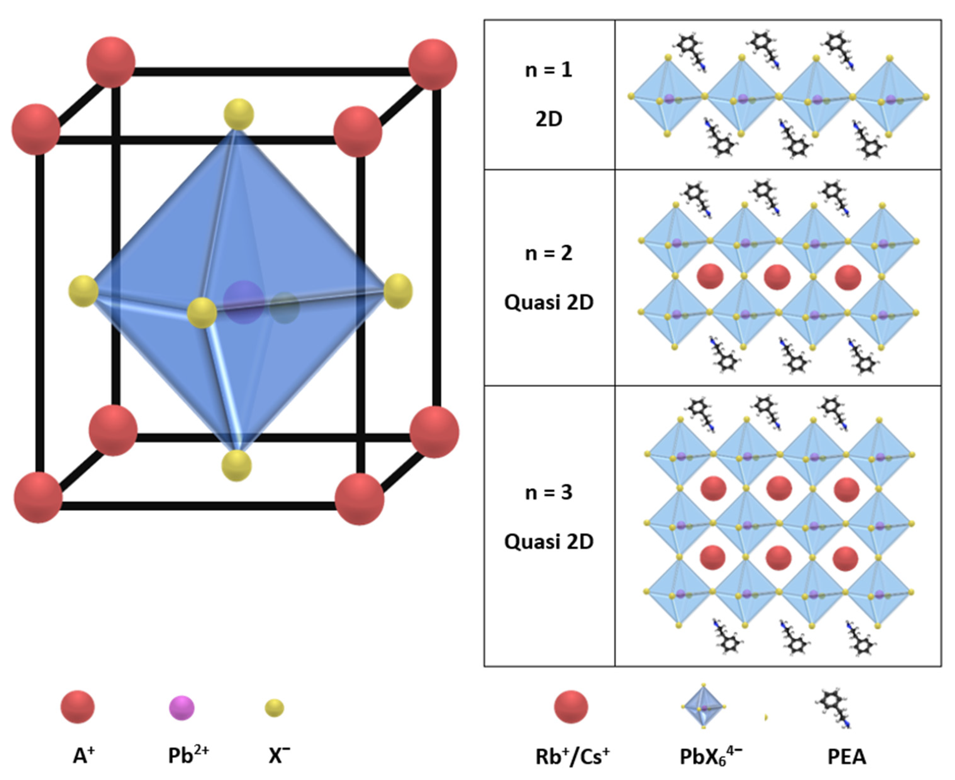
:1. Introduction
2. Materials and Methods
2.1. The Preparation of the Perovskite Solution
2.2. Perovskite Film Fabrication
2.3. Absorbance, Photoluminescence (PL), and Transient Absorption (TA) Measurements
2.4. Cathodoluminescence Imaging
2.5. Data Analysis
3. Results and Discussion
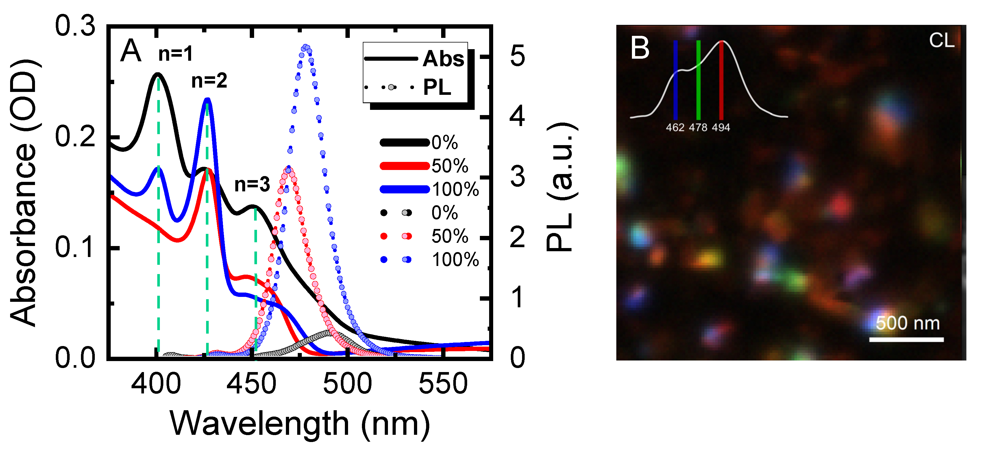
3.1. Steady-State Spectroscopy
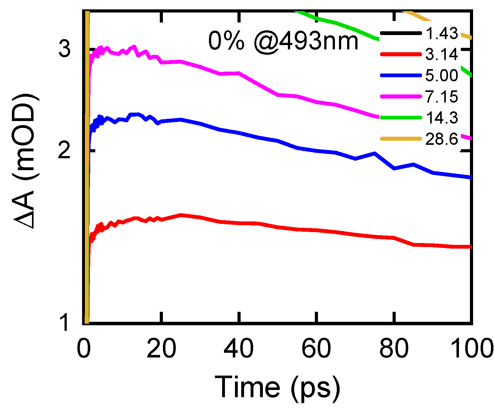
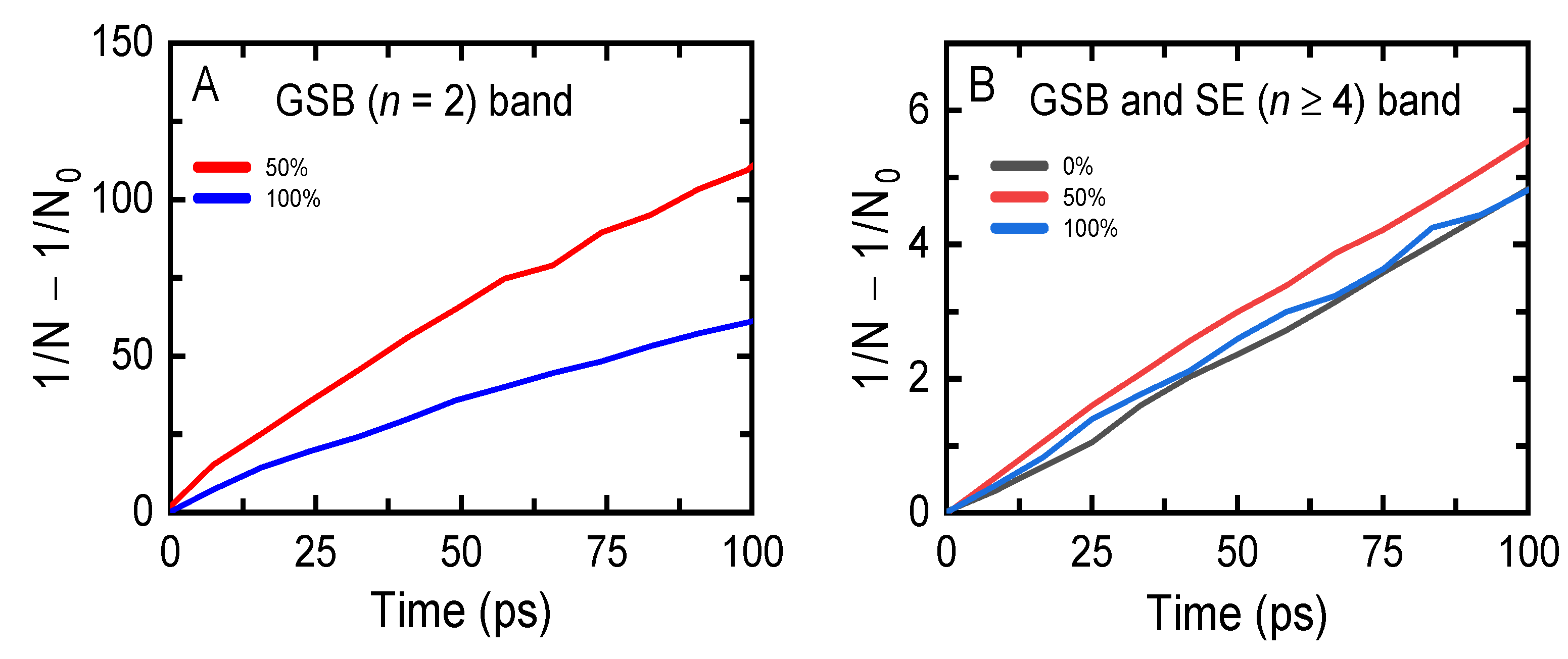
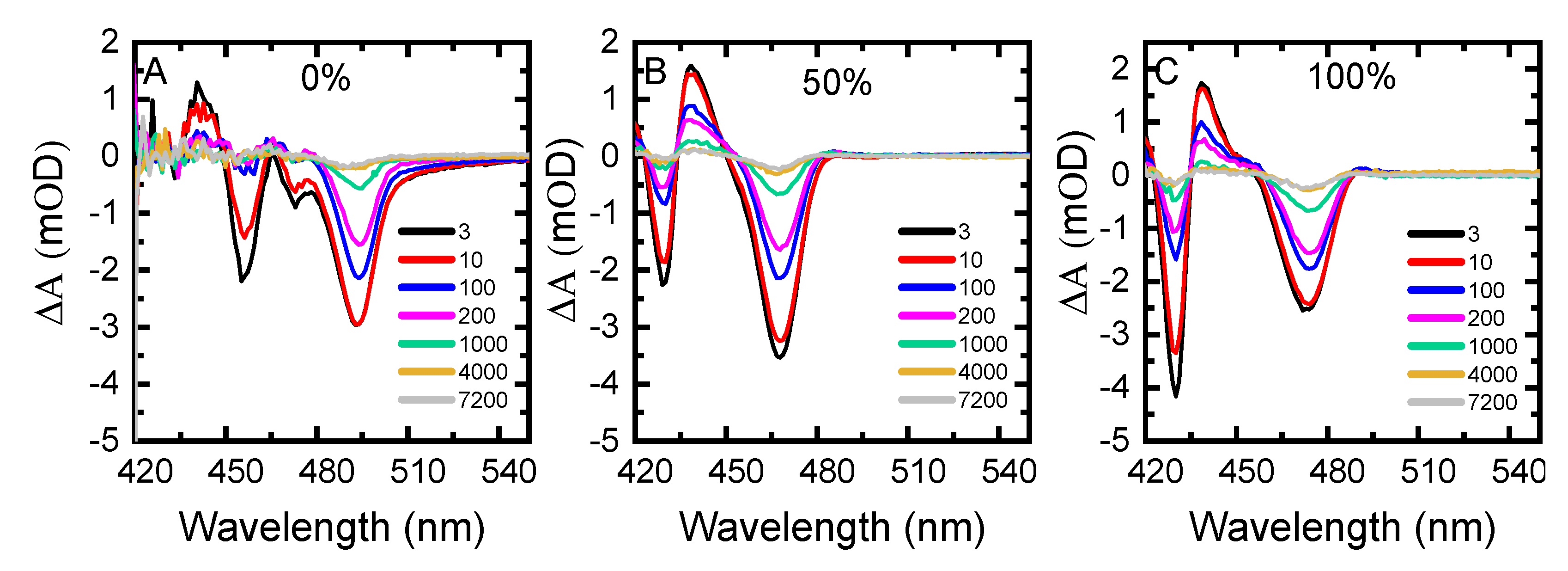
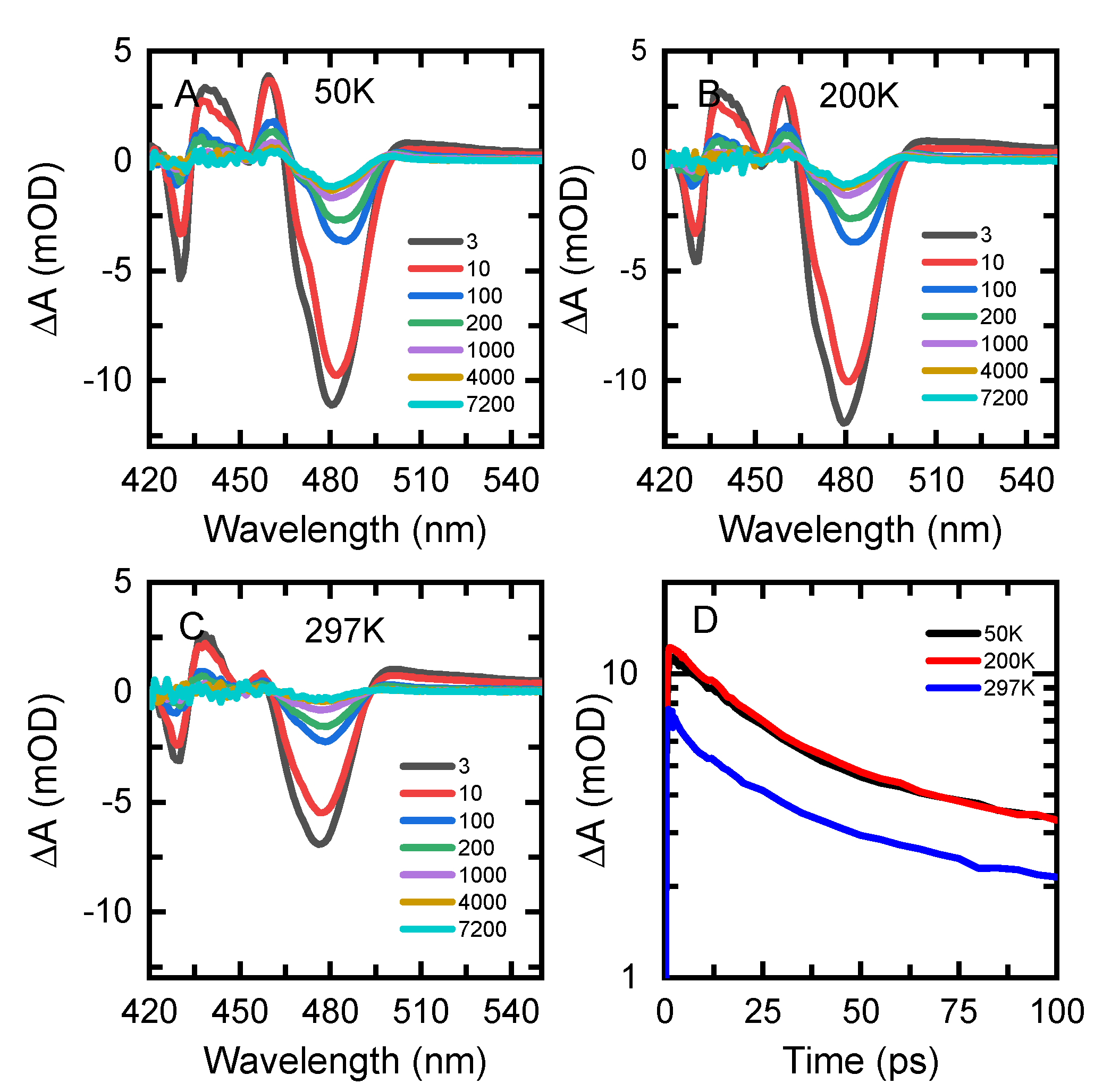
3.2. Transient Absorption Spectroscopy
4. Conclusions
Supplementary Materials
Author Contributions
Funding
Institutional Review Board Statement
Informed Consent Statement
Data Availability Statement
Conflicts of Interest
References
- Ling, Y.; Yuan, Z.; Tian, Y.; Wang, X.; Wang, J.C.; Xin, Y.; Hanson, K.; Ma, B.; Gao, H. Bright Light-Emitting Diodes Based on Organometal Halide Perovskite Nanoplatelets. Adv. Mater. 2016, 28, 305–311. [Google Scholar] [CrossRef] [PubMed]
- Cho, H.; Jeong, S.H.; Park, M.H.; Kim, Y.H.; Wolf, C.; Lee, C.L.; Heo, J.H.; Sadhanala, A.; Myoung, N.S.; Yoo, S.; et al. Overcoming the Electroluminescence Efficiency Limitations of Perovskite Light-Emitting Diodes. Science 2015, 350, 1222–1225. [Google Scholar] [CrossRef] [PubMed]
- Wang, N.; Cheng, L.; Ge, R.; Zhang, S.; Miao, Y.; Zou, W.; Yi, C.; Sun, Y.; Cao, Y.; Yang, R.; et al. Perovskite Light-Emitting Diodes Based on Solution-Processed Self-Organized Multiple Quantum Wells. Nat. Photonics 2016, 10, 699–704. [Google Scholar] [CrossRef]
- Yuan, M.; Quan, L.N.; Comin, R.; Walters, G.; Sabatini, R.; Voznyy, O.; Hoogland, S.; Zhao, Y.; Beauregard, E.M.; Kanjanaboos, P.; et al. Perovskite Energy Funnels for Efficient Light-Emitting Diodes. Nat. Nanotechnol. 2016, 11, 872–877. [Google Scholar] [CrossRef]
- Yang, X.; Zhang, X.; Deng, J.; Chu, Z.; Jiang, Q.; Meng, J.; Wang, P.; Zhang, L.; Yin, Z.; You, J. Efficient Green Light-Emitting Diodes Based on Quasi-Two-Dimensional Composition and Phase Engineered Perovskite with Surface Passivation. Nat. Commun. 2018, 9, 1–8. [Google Scholar] [CrossRef]
- Wang, H.; Zhang, X.; Wu, Q.; Cao, F.; Yang, D.; Shang, Y.; Ning, Z.; Zhang, W.; Zheng, W.; Yan, Y.; et al. Trifluoroacetate Induced Small-Grained CsPbBr 3 Perovskite Films Result in Efficient and Stable Light-Emitting Devices. Nat. Commun. 2019, 10, 665. [Google Scholar] [CrossRef]
- Burschka, J.; Pellet, N.; Moon, S.J.; Humphry-Baker, R.; Gao, P.; Nazeeruddin, M.K.; Grätzel, M. Sequential Deposition as a Route to High-Performance Perovskite-Sensitized Solar Cells. Nature 2013, 499, 316–319. [Google Scholar] [CrossRef]
- Tiwari, A.; Satpute, N.S.; Mehare, C.M.; Dhoble, S.J. Challenges, Recent Advances and Improvements for Enhancing the Efficiencies of ABX3-Based PeLEDs (Perovskites Light Emitting Diodes): A Review. J. Alloys Compd. 2021, 850, 156827. [Google Scholar] [CrossRef]
- Li, Z.; Cao, K.; Li, J.; Tang, Y.; Ding, X.; Yu, B. Review of Blue Perovskite Light Emitting Diodes with Optimization Strategies for Perovskite Film and Device Structure. Opto-Electron. Adv. 2021, 4, 200019. [Google Scholar] [CrossRef]
- Van Le, Q.; Jang, H.W.; Kim, S.Y. Recent Advances toward High-Efficiency Halide Perovskite Light-Emitting Diodes: Review and Perspective. Small Methods 2018, 2, 1700419. [Google Scholar] [CrossRef]
- Liu, Y.; Ono, L.K.; Qi, Y. Organic Additive Engineering toward Efficient Perovskite Light-Emitting Diodes. InfoMat 2020, 2, 1095–1108. [Google Scholar] [CrossRef]
- Liu, X.K.; Xu, W.; Bai, S.; Jin, Y.; Wang, J.; Friend, R.H.; Gao, F. Metal Halide Perovskites for Light-Emitting Diodes. Nat. Mater. 2021, 20, 10–21. [Google Scholar] [CrossRef]
- Wojciechowski, K.; Stranks, S.D.; Abate, A.; Sadoughi, G.; Sadhanala, A.; Kopidakis, N.; Rumbles, G.; Li, C.Z.; Friend, R.H.; Jen, A.K.Y.; et al. Heterojunction Modification for Highly Efficient Organic-Inorganic Perovskite Solar Cells. ACS Nano 2014, 8, 12701–12709. [Google Scholar] [CrossRef]
- Cao, Y.; Wang, N.; Tian, H.; Guo, J.; Wei, Y.; Chen, H.; Miao, Y.; Zou, W.; Pan, K.; He, Y.; et al. Perovskite Light-Emitting Diodes Based on Spontaneously Formed Submicrometre-Scale Structures. Nature 2018, 562, 249–253. [Google Scholar] [CrossRef]
- Chiba, T.; Hayashi, Y.; Ebe, H.; Hoshi, K.; Sato, J.; Sato, S.; Pu, Y.-J.; Ohisa, S.; Kido, J. Anion-Exchange Red Perovskite Quantum Dots with Ammonium Iodine Salts for Highly Efficient Light-Emitting Devices. Nat. Photonics 2018, 12, 681–687. [Google Scholar] [CrossRef]
- Kim, Y.-H.; Kim, S.; Kakekhani, A.; Park, J.; Park, J.; Lee, Y.-H.; Xu, H.; Nagane, S.; Wexler, R.B.; Kim, D.-H.; et al. Comprehensive Defect Suppression in Perovskite Nanocrystals for High-Efficiency Light-Emitting Diodes. Nat. Photonics 2021, 15, 148–155. [Google Scholar] [CrossRef]
- Chu, Z.; Zhao, Y.; Ma, F.; Zhang, C.X.; Deng, H.; Gao, F.; Ye, Q.; Meng, J.; Yin, Z.; Zhang, X.; et al. Large Cation Ethylammonium Incorporated Perovskite for Efficient and Spectra Stable Blue Light-Emitting Diodes. Nat. Commun. 2020, 11, 4165. [Google Scholar] [CrossRef]
- Luoa, D.; Chen, Q.; Qiu, Y.; Zhang, M.; Liu, B. Device Engineering for All-Inorganic Perovskite Light-Emitting Diodes. Nanomaterials 2019, 9, 1007. [Google Scholar] [CrossRef]
- Yang, X.; Zhou, G.; Wong, W.Y. Functionalization of Phosphorescent Emitters and Their Host Materials by Main-Group Elements for Phosphorescent Organic Light-Emitting Devices. Chem. Soc. Rev. 2015, 44, 8484–8575. [Google Scholar] [CrossRef]
- Jou, J.H.; Kumar, S.; Agrawal, A.; Li, T.H.; Sahoo, S. Approaches for Fabricating High Efficiency Organic Light Emitting Diodes. J. Mater. Chem. C 2015, 3, 2974–3002. [Google Scholar] [CrossRef]
- Liu, B.; Li, X.L.; Tao, H.; Zou, J.; Xu, M.; Wang, L.; Peng, J.; Cao, Y. Manipulation of Exciton Distribution for High-Performance Fluorescent/Phosphorescent Hybrid White Organic Light-Emitting Diodes. J. Mater. Chem. C 2017, 5, 7668–7683. [Google Scholar] [CrossRef]
- Zhang, X.; Lin, H.; Huang, H.; Reckmeier, C.; Zhang, Y.; Choy, W.C.H.; Rogach, A.L. Enhancing the Brightness of Cesium Lead Halide Perovskite Nanocrystal Based Green Light-Emitting Devices through the Interface Engineering with Perfluorinated Ionomer. Nano Lett. 2016, 16, 1415–1420. [Google Scholar] [CrossRef]
- Xiao, Z.; Kerner, R.A.; Zhao, L.; Tran, N.L.; Lee, K.M.; Koh, T.W.; Scholes, G.D.; Rand, B.P. Efficient Perovskite Light-Emitting Diodes Featuring Nanometre-Sized Crystallites. Nat. Photonics 2017, 11, 108–115. [Google Scholar] [CrossRef]
- Li, J.; Xu, L.; Wang, T.; Song, J.; Chen, J.; Xue, J.; Dong, Y.; Cai, B.; Shan, Q.; Han, B.; et al. 50-Fold EQE Improvement up to 6.27% of Solution-Processed All-Inorganic Perovskite CsPbBr3 QLEDs via Surface Ligand Density Control. Adv. Mater. 2017, 29, 1603885. [Google Scholar] [CrossRef]
- Na Quan, L.; Ma, D.; Zhao, Y.; Voznyy, O.; Yuan, H.; Bladt, E.; Pan, J.; García de Arquer, F.P.; Sabatini, R.; Piontkowski, Z.; et al. Edge Stabilization in Reduced-Dimensional Perovskites. Nat. Commun. 2020, 11, 170. [Google Scholar] [CrossRef]
- Jiang, Y.; Qin, C.; Cui, M.; He, T.; Liu, K.; Huang, Y.; Luo, M.; Zhang, L.; Xu, H.; Li, S.; et al. Spectra Stable Blue Perovskite Light-Emitting Diodes. Nat. Commun. 2019, 10, 1868. [Google Scholar] [CrossRef]
- Xu, L.J.; Worku, M.; He, Q.; Ma, B. Advances in Light-Emitting Metal-Halide Perovskite Nanocrystals. MRS Bull. 2020, 45, 458–466. [Google Scholar] [CrossRef]
- Kumawat, N.K.; Liu, X.-K.; Kabra, D.; Gao, F. Blue Perovskite Light-Emitting Diodes: Progress, Challenges and Future Directions. Nanoscale 2019, 11, 2109–2120. [Google Scholar] [CrossRef]
- Fakharuddin, A.; Franckevičius, M.; Devižis, A.; Gelžinis, A.; Chmeliov, J.; Heremans, P.; Gulbinas, V. Double Charge Transfer Dominates in Carrier Localization in Low Bandgap Sites of Heterogeneous Lead Halide Perovskites. Adv. Funct. Mater. 2021, 31, 2010076. [Google Scholar] [CrossRef]
- Baldwin, A.; Delport, G.; Leng, K.; Chahbazian, R.; Galkowski, K.; Loh, K.P.; Stranks, S.D. Local Energy Landscape Drives Long-Range Exciton Diffusion in Two-Dimensional Halide Perovskite Semiconductors. J. Phys. Chem. Lett. 2021, 12, 4003–4011. [Google Scholar] [CrossRef]
- Liu, J.; Leng, J.; Wu, K.; Zhang, J.; Jin, S. Observation of Internal Photoinduced Electron and Hole Separation in Hybrid Two-Dimentional Perovskite Films. J. Am. Chem. Soc. 2017, 139, 1432–1435. [Google Scholar] [CrossRef] [PubMed]
- Mondal, N.; Naphade, R.; Zhou, X.; Zheng, Y.; Lee, K.; Gereige, I.; Al-Saggaf, A.; Bakr, O.M.; Mohammed, O.F.; Gartstein, Y.N.; et al. Dynamical Interconversion between Excitons and Geminate Charge Pairs in Two-Dimensional Perovskite Layers Described by the Onsager–Braun Model. J. Phys. Chem. Lett. 2020, 11, 1112–1119. [Google Scholar] [CrossRef] [PubMed]
- Spitha, N.; Kohler, D.D.; Hautzinger, M.P.; Li, J.; Jin, S.; Wright, J.C. Discerning between Exciton and Free-Carrier Behaviors in Ruddlesden–Popper Perovskite Quantum Wells through Kinetic Modeling of Photoluminescence Dynamics. J. Phys. Chem. C 2020, 124, 17430–17439. [Google Scholar] [CrossRef]
- Deng, S.; Shi, E.; Yuan, L.; Jin, L.; Dou, L.; Huang, L. Long-Range Exciton Transport and Slow Annihilation in Two-Dimensional Hybrid Perovskites. Nat. Commun. 2020, 11, 664. [Google Scholar] [CrossRef] [PubMed]
- Blancon, J.-C.; Tsai, H.; Nie, W.; Stoumpos, C.C.; Pedesseau, L.; Katan, C.; Kepenekian, M.; Soe, C.M.M.; Appavoo, K.; Sfeir, M.Y.; et al. Extremely Efficient Internal Exciton Dissociation through Edge States in Layered 2D Perovskites. Science 2017, 355, 1288–1292. [Google Scholar] [CrossRef] [PubMed]
- Shang, Q.; Wang, Y.; Zhong, Y.; Mi, Y.; Qin, L.; Zhao, Y.; Qiu, X.; Liu, X.; Zhang, Q. Unveiling Structurally Engineered Carrier Dynamics in Hybrid Quasi-Two-Dimensional Perovskite Thin Films toward Controllable Emission. J. Phys. Chem. Lett. 2017, 8, 4431–4438. [Google Scholar] [CrossRef] [PubMed]
- Blancon, J.-C.; Stier, A.V.; Tsai, H.; Nie, W.; Stoumpos, C.C.; Traoré, B.; Pedesseau, L.; Kepenekian, M.; Katsutani, F.; Noe, G.T.; et al. Scaling Law for Excitons in 2D Perovskite Quantum Wells. Nat. Commun. 2018, 9, 2254. [Google Scholar] [CrossRef]
- Abhishek, K.; Ankur, S.; Manukumara, M.; Sankaran, R.; Kumar, S.Y.; Piyush, A.; Chien, S.T.; Ranjan, S. Excitons in 2D Perovskites for Ultrafast Terahertz Photonic Devices. Sci. Adv. 2022, 6, eaax8821. [Google Scholar]
- Delport, G.; Chehade, G.; Lédeé, F.; Diab, H.; Milesi-Brault, C.; Trippé-Allard, G.; Even, J.; Lauret, J.S.; Deleporte, E.; Garrot, D. Exciton-Exciton Annihilation in Two-Dimensional Halide Perovskites at Room Temperature. J. Phys. Chem. Lett. 2019, 10, 5153–5159. [Google Scholar] [CrossRef]
- Villamil Franco, C.; Mahler, B.; Cornaggia, C.; Gustavsson, T.; Cassette, E. Auger Recombination and Multiple Exciton Generation in Colloidal Two-Dimensional Perovskite Nanoplatelets: Implications for Light-Emitting Devices. ACS Appl. Nano Mater. 2021, 4, 558–567. [Google Scholar] [CrossRef]
- Lu, J.; Chen, W.; Zhou, C.; Yang, S.; Wang, C.; Wang, R.; Wang, X.; Gan, Z.; Jia, B.; Wen, X. Layer Number Dependent Exciton Dissociation and Carrier Recombination in 2D Ruddlesden–Popper Halide Perovskites. J. Mater. Chem. C 2021, 9, 8966–8974. [Google Scholar] [CrossRef]
- Lian, X.; Wang, X.; Ling, Y.; Lochner, E.; Tan, L.; Zhou, Y.; Ma, B.; Hanson, K.; Gao, H. Light Emitting Diodes Based on Inorganic Composite Halide Perovskites. Adv. Funct. Mater. 2019, 29, 1807345. [Google Scholar] [CrossRef]
- Liashenko, T.G.; Pushkarev, A.P.; Naujokaitis, A.; Pakštas, V.; Franckevičius, M.; Zakhidov, A.A.; Makarov, S.V. Suppression of Electric Field-Induced Segregation in Sky-Blue Perovskite Light-Emitting Electrochemical Cells. Nanomaterials 2020, 10, 1937. [Google Scholar] [CrossRef]
- Peng, X.; Yan, C.; Chun, F.; Li, W.; Fu, X.; Yang, W. A Review of Low-Dimensional Metal Halide Perovskites for Blue Light Emitting Diodes. J. Alloys Compd. 2021, 883, 160727. [Google Scholar] [CrossRef]
- Wang, K.; Park, J.Y.; Akriti; Dou, L. Two-Dimensional Halide Perovskite Quantum-Well Emitters: A Critical Review. EcoMat 2021, 3, e12104. [Google Scholar] [CrossRef]
- Kumar, G.S.; Sumukam, R.R.; Murali, B. Quasi-2D Perovskite Emitters: A Boon for Efficient Blue Light-Emitting Diodes. J. Mater. Chem. C 2020, 8, 14334–14347. [Google Scholar] [CrossRef]
- Litvinas, D.; Aleksiejūnas, R.; Ščajev, P.; Baronas, P.; Soriūtė, V.; Qin, C.; Fujihara, T.; Matsushima, T.; Adachi, C.; Juršėnas, S. Energy Transfer in (PEA)2FAn−1PbnBr3n+1 quasi-2D Perovskites. J. Mater. Chem. C 2021, 9, 4782–4791. [Google Scholar] [CrossRef]


| Excess of RbBr Content | Peak PL Wavelength (nm) | Peak PL Photon Energy (eV) | Spectral Width at FWHM (nm) |
|---|---|---|---|
| 0% | 490 | 2.53 | 30 |
| 50% | 469 | 2.64 | 21 |
| 100% | 478 | 2.59 | 22 |
Publisher’s Note: MDPI stays neutral with regard to jurisdictional claims in published maps and institutional affiliations. |
© 2022 by the authors. Licensee MDPI, Basel, Switzerland. This article is an open access article distributed under the terms and conditions of the Creative Commons Attribution (CC BY) license (https://creativecommons.org/licenses/by/4.0/).
Share and Cite
Abdelrazik, L.; Jašinskas, V.; Podlipskas, Ž.; Aleksiejūnas, R.; Tamulaitis, G.; Gulbinas, V.; Vyšniauskas, A. Exciton Transfer Dynamics and Annihilation in Rubidium–Cesium-Alloyed, Quasi-Two-Dimensional Perovskite. Photonics 2022, 9, 578. https://doi.org/10.3390/photonics9080578
Abdelrazik L, Jašinskas V, Podlipskas Ž, Aleksiejūnas R, Tamulaitis G, Gulbinas V, Vyšniauskas A. Exciton Transfer Dynamics and Annihilation in Rubidium–Cesium-Alloyed, Quasi-Two-Dimensional Perovskite. Photonics. 2022; 9(8):578. https://doi.org/10.3390/photonics9080578
Chicago/Turabian StyleAbdelrazik, Lamiaa, Vidmantas Jašinskas, Žydrūnas Podlipskas, Ramūnas Aleksiejūnas, Gintautas Tamulaitis, Vidmantas Gulbinas, and Aurimas Vyšniauskas. 2022. "Exciton Transfer Dynamics and Annihilation in Rubidium–Cesium-Alloyed, Quasi-Two-Dimensional Perovskite" Photonics 9, no. 8: 578. https://doi.org/10.3390/photonics9080578
APA StyleAbdelrazik, L., Jašinskas, V., Podlipskas, Ž., Aleksiejūnas, R., Tamulaitis, G., Gulbinas, V., & Vyšniauskas, A. (2022). Exciton Transfer Dynamics and Annihilation in Rubidium–Cesium-Alloyed, Quasi-Two-Dimensional Perovskite. Photonics, 9(8), 578. https://doi.org/10.3390/photonics9080578