Article

Silicon-on-Insulator Optical Buffer Based on Magneto-Optical 1 × 3 Micro-Rings Array Coupled Sagnac Ring

Institute of Optical Information, Key Laboratory of Luminescence and Optical Information, Ministry of Education, School of Physical Science and Engineering, Beijing Jiaotong University, Beijing 100044, China
*
Author to whom correspondence should be addressed.
Photonics 2022, 9(6), 366; https://doi.org/10.3390/photonics9060366
Submission received: 6 April 2022 / Revised: 14 May 2022 / Accepted: 20 May 2022 / Published: 24 May 2022

Abstract

:
Optical buffer is a key technology to control optical routing and solve channel competition, which directly determines the performance of information processing and storage. In this study, a switchable optical buffer using the nonreciprocal silicon-on-insulator (SOI) magneto-optical micro-ring (MOMR) array coupled with Sagnac ring was introduced, which can exceed the time-bandwidth limitation. The transmission equations and propagation characteristics of optical signal in 1 × 3 micro-rings and Sagnac ring coupled 1 × 3 micro-rings based on two kinds of phase-change materials were studied. The group time delay, effective buffer time and readout operation in the buffer were also investigated.

1. Introduction

Optical buffer plays an important role in optical packet switching networks, which can not only provide an adjustable buffering time for nodes to process the frame header, but also solve the competition problem of the same port. The current method of optical buffer devotes to delay the optical signal in the light-guiding medium for a period of time. Optical buffer can be realized by slowing down the propagation speed of light and extending the length of transmission medium. Therefore, optical buffers can be divided into three categories: buffers using slow light effects [1,2,3,4]; buffers based on photonic crystal (PhC) structure [5,6,7,8], including PhC cavities [6] and slotted PhC waveguides [7]; and buffers based on optical structures, including optical fiber delay-line structure [9,10,11] and optical micro-ring resonator structure [12,13]. Recently, more and more attention has been paid to the silicon-based optical buffers for miniaturization and integration. The PhC cavities with ultra-high Q-factors and ultra-small mode volumes can be used for the design of the optical buffers with ultrafast response speed and an extremely compact size [6]. The slotted PhC waveguide has the characteristics of compact size, high sensitivity and low coupling losses [7], which can be used in all-optical buffers with low dispersion, distortion and attenuation [8]. As a miniaturized device that can be easily integrated into microsystems, more and more ring resonators are widely used in integrated system. For example, Kalantarov et al. [14] reported tunable optical delay line using three coupled micro-ring (MR) resonators. Guo et al. [15] investigated an optical storage device based on two mutually coupled ring resonators, with one ring coupled to two waveguides. Additionally, Ni et al. [16] reported a Sagnac optical switch chip using two serial MOMRs array. Fan et al. [17] reported an optical buffer device based on VO2 films embedded on SOI waveguide micro-ring resonator due to phase transition characteristics of VO2. Kumar et al. [18] implemented an all-optical 1 × 4 memory register unit using the micro-ring resonator structures.
However, there is an important problem with all types of optical buffer, which is that they are limited by time-bandwidth limitation [19]. The time-bandwidth limitation is characterizing the storage capacity of all linear, time-invariant resonant and wave-guiding devices. For any type of system, the time delays ∆t is inversely proportional to its bandwidth ∆ω, ∆t∙∆ω~2π. For an optical buffer, it cannot store large data for a long time. However, Lorentz reciprocity can be broken by using non-reciprocal magneto-optical (MO) waveguides in devices to overcome this limit [20,21]. Phase-change materials (PCM) show a difference in both optical and electronic properties between two stable solid phases, amorphous (AM) and crystalline (CR) states. Under appropriate thermal, electrical or optical stimulation, they can reversibly cycle between these states with high reproducibility and long-term stability [22]. Several beneficial properties of PCMs are exploited to yield more compact switches [23,24].
In this paper, a SOI 1 × 3 MOMR array coupled with Sagnac ring was designed to realize the function of an optical buffer. The non-reciprocal MO waveguide was used to break the time-bandwidth limitation. The PCM on one of the rings was used to realize the readout control of the optical buffer. The transmission equations of the three MOMRs coupled straight waveguide and three MOMRs coupled Sagnac ring were derived respectively. The transmission spectrum of 1 × 3 MOMRs coupling structure and Sagnac ring with 1 × 3 MOMRs based on two kinds of PCM in crystalline and amorphous states are calculated. The buffering time, write-in and read-out operation in this optical buffer were discussed. The results of this study are of great significance to the design and application of the optical buffer with MO waveguides.

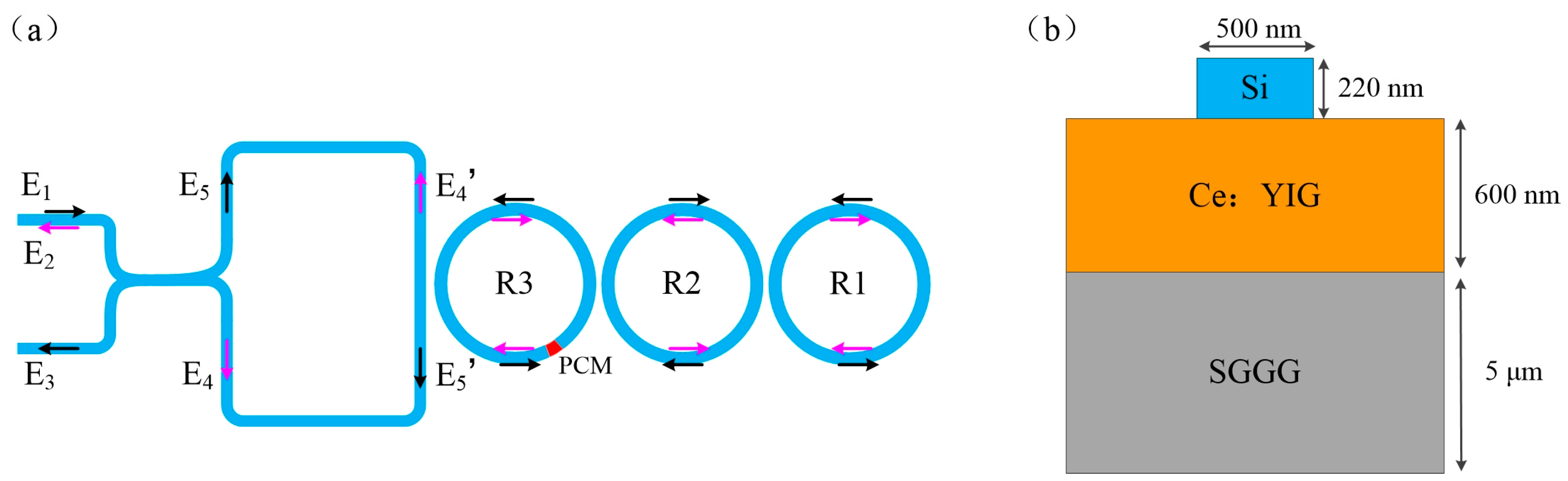
2. SOI Optical Buffer Based on Sagnac Ring Coupled with MOMR Array

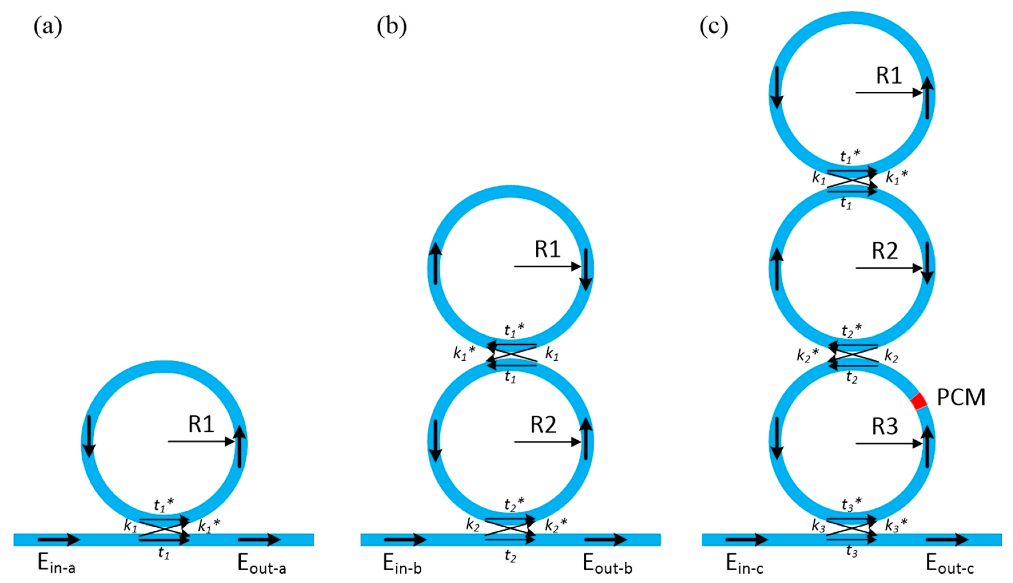
2.1. Sagnac Ring with 1 × 3 MOMRs

Figure 1a shows the structure of the optical buffer. It consists of a Sagnac ring and the MOMR array structure. The PCM is placed in the uncoupled region of the third micro-ring, as shown in red region of R3. The optical signal is launched into the silicon waveguide and divided into two light beams propagating clockwise and counterclockwise in the Sagnac ring. Figure 1b shows the section diagram of the micro-ring array in a three-layer non-reciprocal MO waveguide structure. It consists of one dielectric layer (silicon) and two MO layers, cerium-substituted yttrium iron garnet (Ce–YIG) and substituted gadolinium gallium garnet (SGGG). The external magnetic field is applied in the direction which is perpendicular to the direction of light transmission, and gives rise to the resulting nonreciprocal phase shift (NRPS).

2.2. Nonreciprocal Phase Shift (NRPS) of the SOI Nonreciprocal MO Waveguide

Because of the effect of magnetic field bias, the properties of MO materials will change. The damage of the Lorentz reciprocity in the waveguide system originates from the off-diagonal elements in the dielectric tensor of the MO layer. When electromagnetic waves propagate in MO materials, the bias magnetic field and the electrical displacement vector are not in the same direction caused by the Faraday rotation effect, so the anti-angle elements of the second-order matrix of the dielectric tensor are asymmetric. This asymmetry makes electromagnetic waves nonreciprocal when propagating in specific directions in MO materials. For the forward and backward propagation fields, the dielectric tensor of MO material Ce:YIG is expressed as follows [25,26]:
ε f o r w a r d = ( n 2 0 0 0 n 2 j γ 0 j γ n 2 )
ε b a c k w a r d = ( n 2 0 0 0 n 2 j γ 0 j γ n 2 )
where γ is related to the specific Faraday rotation coefficient θ f by γ = 2 n θ F k 0 , k 0 is the wave number of electromagnetic waves in vacuum. The difference of the dielectric tensor in the two propagation directions makes the propagation constant different in the two propagation directions, which is NRPS [27].
N R P S = Δ β = 2 ω ε 0 P E * Δ ε E d x d y
where P = ( E × H * + E * × H ) z d x d y is the normalized energy flow density. ∆ε is the gyrotropic part of the permittivity tensor.

2.3. Mathematical Model

The transmission matrix is shown in Equation (4) when a micro-ring is coupled with a straight waveguide, as shown in Figure 2a. k1 and k1* are the amplitude coupling coefficients between the micro-ring and the straight waveguide, t1 and t1* are the amplitude transmission coefficients, and | k 2 | + | t 2 | = 1 .
[ E out - a E out - a ] = [ t 1 k 1 k 1 * t 1 * ] [ E in - a E in - a ]
The electric field changes to E in - a = e α 1 L 1 e j β L 1 E out - a as the light travels around the ring. L1 is the circumference of the micro-ring. α is the attenuation coefficient of micro-ring waveguide. The transfer constant is β = 2 π n e f f / λ , in which neff is the effective refractive index of the micro-ring, and λ is the wavelength of incident light. The following formula can be obtained from the transmission matrix.
For N 1 = e α 1 L 1 e j β L 1 , the transfer function T1 from input to output can be expressed as:
T 1 = E out - a E in - a = t 1 N 1 1 t 1 * N 1
Similarly, a straight waveguide coupled with two and three series micro-rings is shown in Figure 2b,c. k2 and k3 represent the coupling rates between the first-second and second-third micro-ring resonators, respectively, and t2 and t3 are the amplitude transmission coefficients. The transfer function from input to output can be expressed as
T 2 = E out - b E in - b = t 2 N 2 1 t 2 * N 2
T 3 = E out - c E in - c = t 3 N 3 1 t 3 * N 3
The optical field transmission coefficient of two series micro-rings is N 2 = T 1 e α 2 L 2 e j β L 2 . L2 and L3 are the circumferences of the micro-rings R2 and R3 respectively. As a phase change material waveguide with length LPCM is added into ring R3, the optical field transmission coefficient of the third series micro-ring becomes N 3 = T 2 e α 3 ( L 3 L P C M ) e j β ( L 3 L P C M ) e α P C M L P C M e j β P C M L P C M , where β P C M = 2 π n e f f P C M / λ .
A straight waveguide coupled with three series micro-rings is shown in Figure 2c, the transfer function from input to output can be expressed as:
T 3 = E out - c E in - c = t 3 T 2 e α 3 ( L 3 L P C M ) e j β ( L 3 L P C M ) e α P C M L P C M e j β P C M L P C M 1 t 3 * T 2 e α 3 ( L 3 L P C M ) e j β ( L 3 L P C M ) e α P C M L P C M e j β P C M L P C M
Figure 1 shows the transmission of optical signal in the Sagnac ring coupled 1 × 3 MOMRs structure. The input signal light field is divided into two light waves by a coupler with a straight-through efficiency of ρ. E1 is the incident optical field, E2 is the reflected optical field, E3 is the transmitted optical field. The clockwise and counterclockwise transmission optical fields in the Sagnac ring are E4 and E5, respectively.
( E 4 E 5 ) = ( ρ i 1 ρ i 1 ρ ρ ) ( 0 E 1 )
After the two light fields go through a round trip in the micro-rings and reach the coupler, the clockwise and counterclockwise transmission light fields become the following formula.
( E 4 E 5 ) = ( T 3 ( β b ) 0 0 T 3 ( β f ) ) ( E 4 E 5 )
T3(βf) and T3(βb) are the transfer functions of the guiding wave light field propagating forward and backward in the 1 × 3 micro-rings in Equation (8), and βf = β0 + Δβ and βb = β0 −Δβ are the corresponding propagation constants. Using the transmission matrix of the coupler again, the reflected and transmitted light field can be obtained as:
( E 2 E 3 ) = ( ρ i 1 ρ i 1 ρ ρ ) ( E 4 E 5 )
The reflected and transmitted optical fields of the Sagnac ring can be obtained by using the transmission matrix of couplers in the Sagnac ring (Equations (9)–(11)).
T = | E 3 E 1 | 2 = | ρ T 3 ( β f ) ( 1 ρ ) T 3 ( β b ) | 2
R = | E 2 E 1 | 2 = | i 1 ρ ρ T 3 ( β b ) + i 1 ρ ρ T 3 ( β f ) | 2

3. Results and Discussion

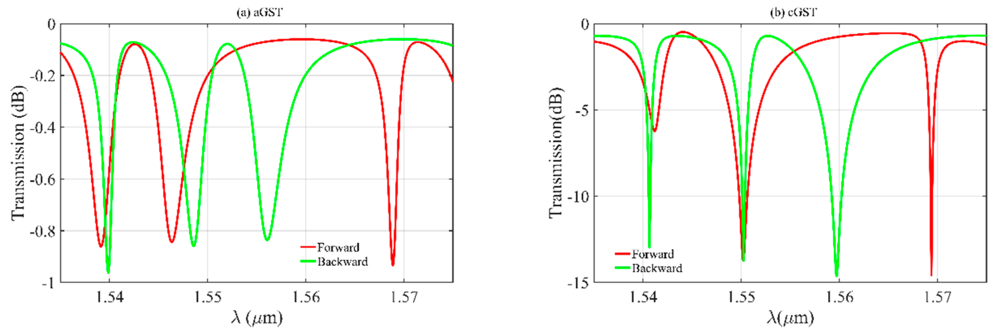
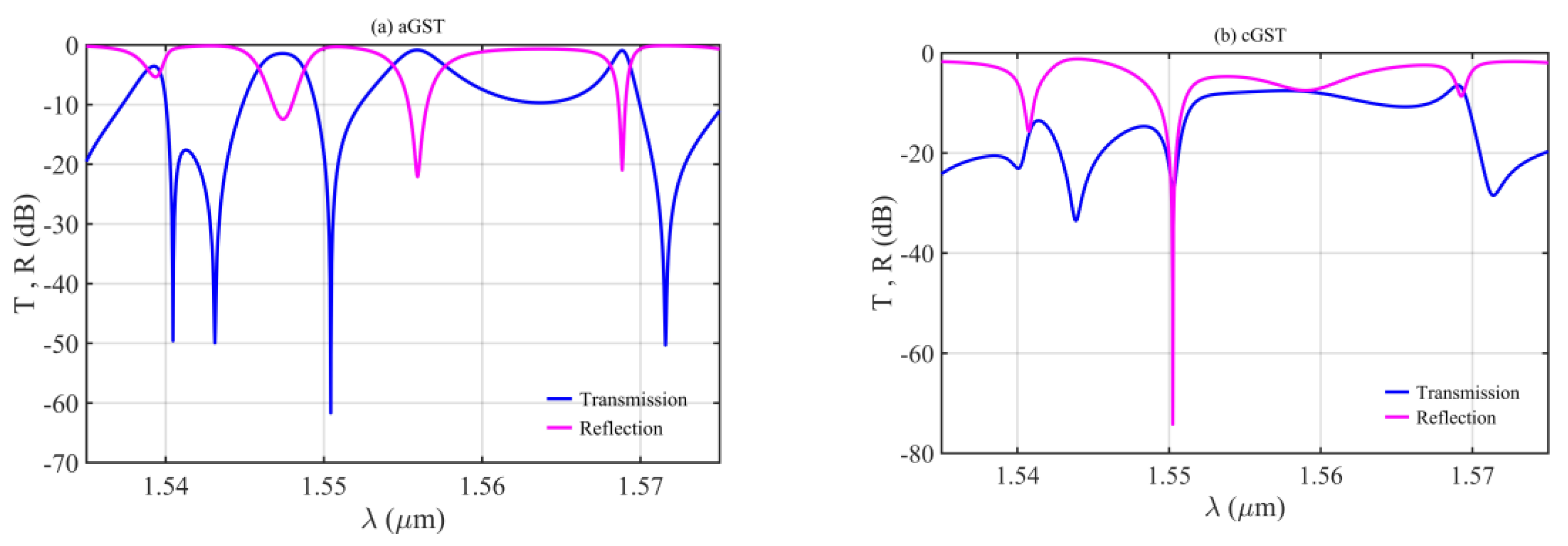
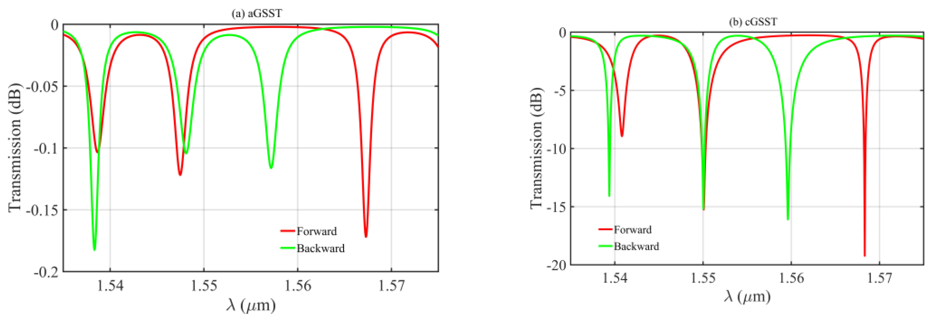
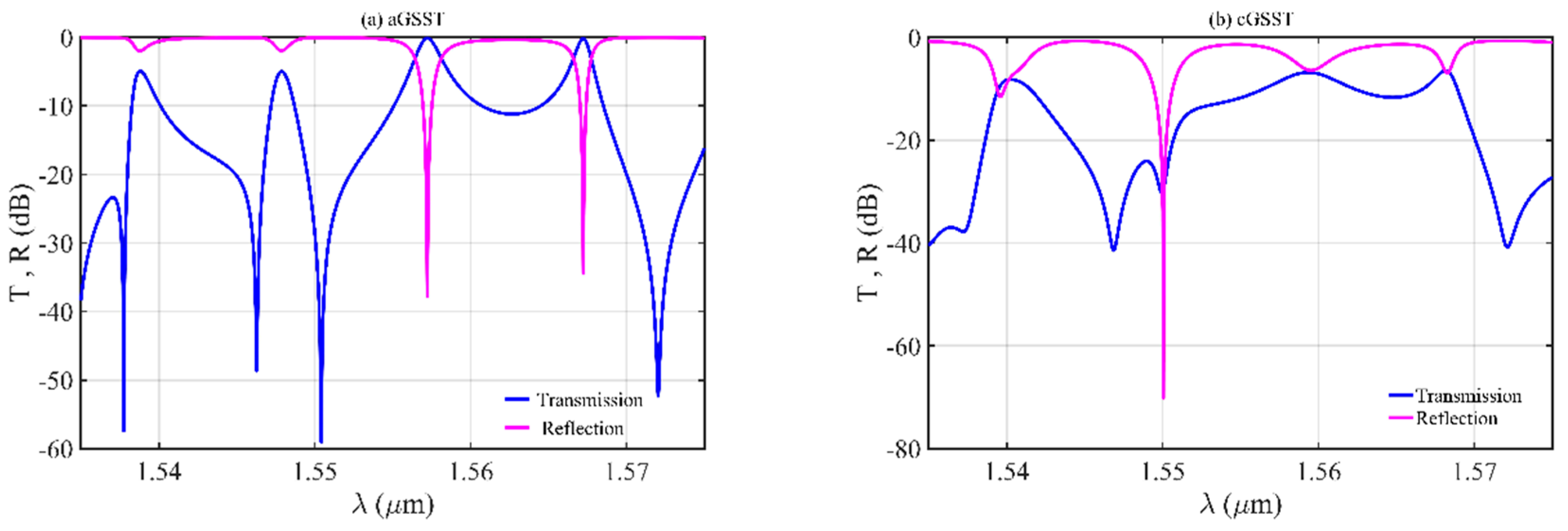
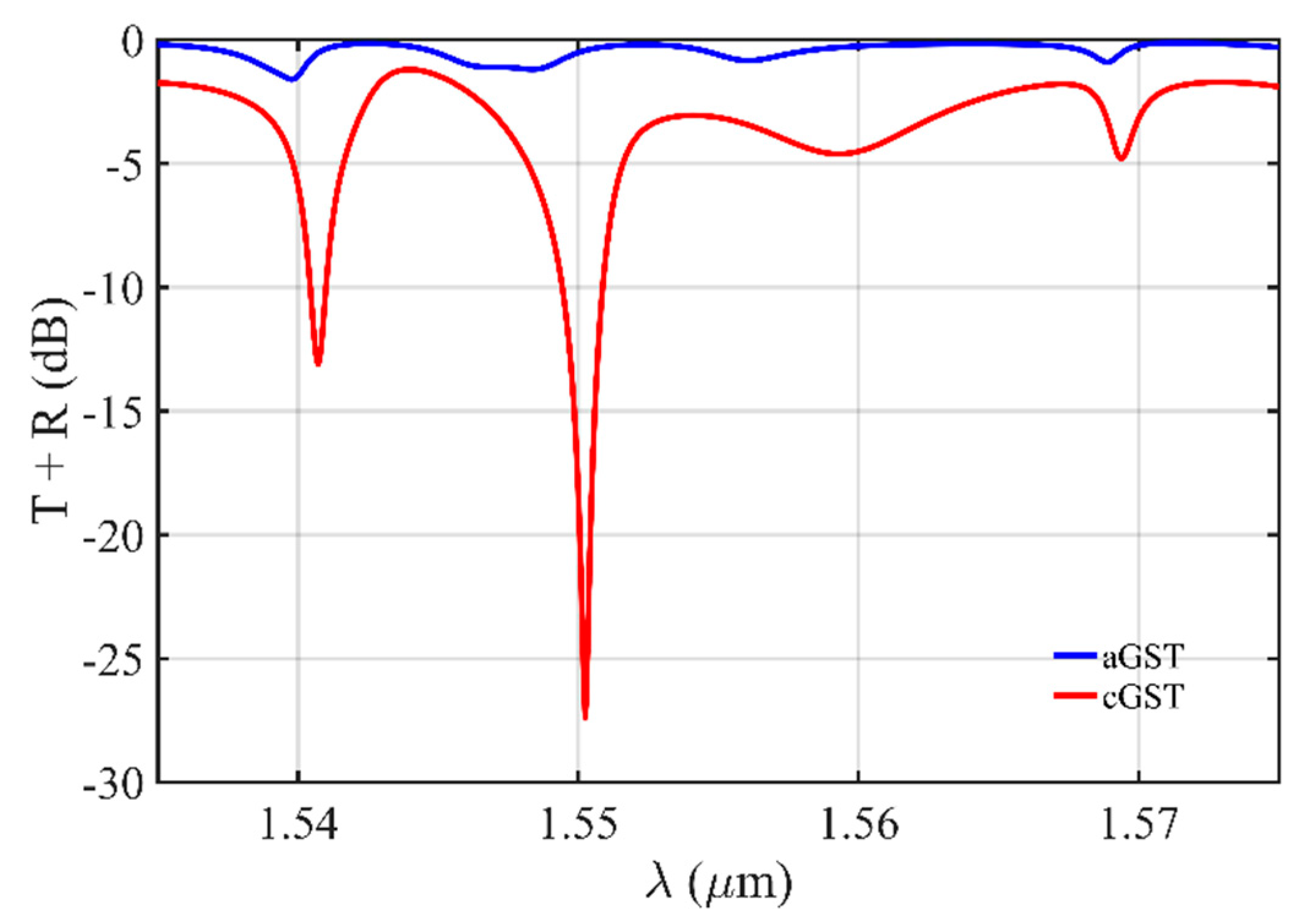
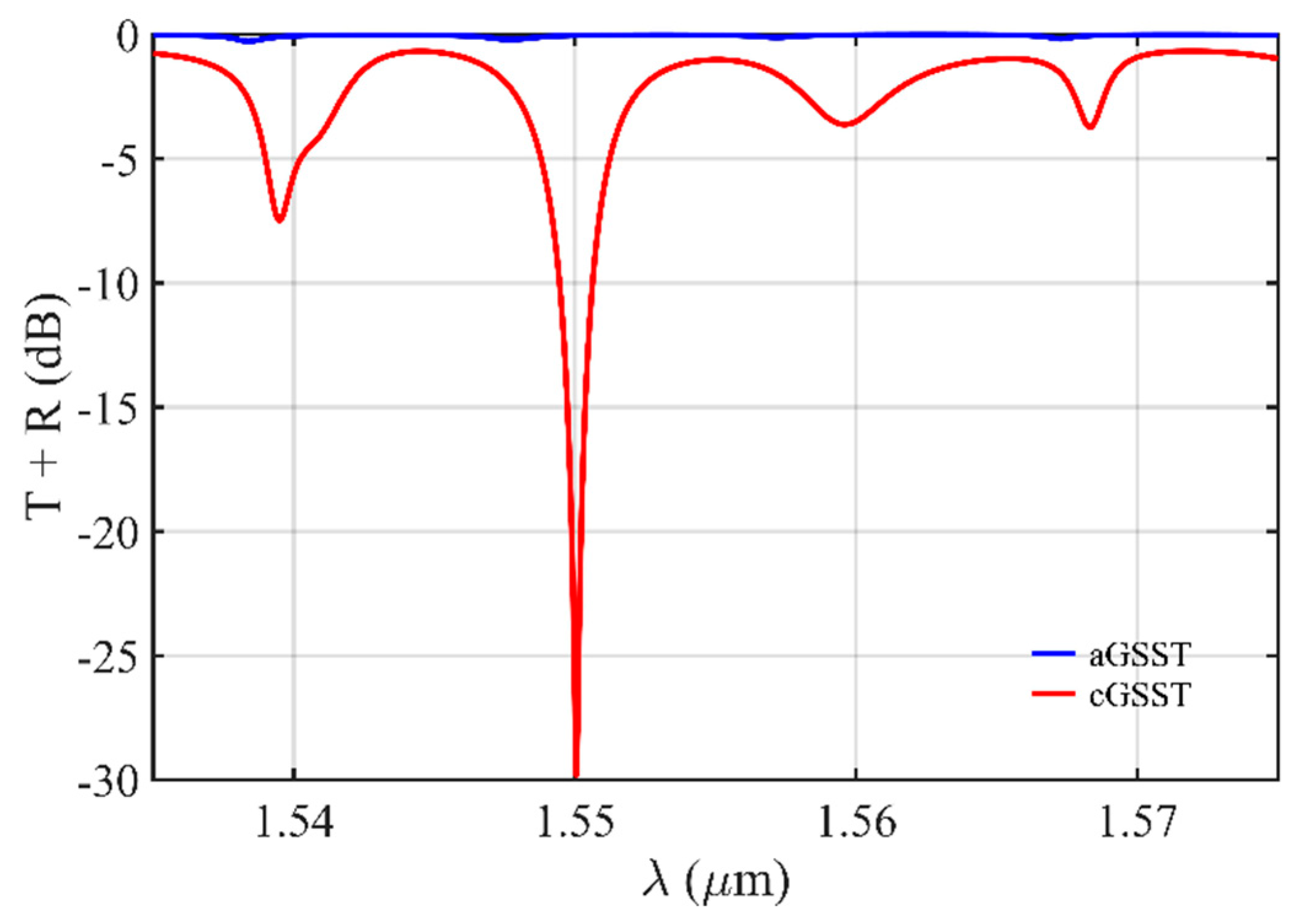
3.1. Transmission Characteristic Analysis

In the three MOMRs structure, the PCM embedded on the surface of the third ring R3 is Ge2Sb2Te5 (GST) or Ge2Sb2Se4Te (GSST) with a thickness of 10 nm and a length of 0.5 μm. In the calculation, the refractive indexes of GST are 3.94 (amorphous) and 6.11 (crystalline) at 1550 nm wavelength, and the extinction coefficients are 0.045 (amorphous) and 0.83 (crystalline) at 1550 nm wavelength [28]. The refractive indexes of GSST are 3.32 (amorphous) and 5.08 (crystalline) at 1550 nm wavelength, and the extinction coefficients are 0 (amorphous) and 0.35 (crystalline) at 1550 nm wavelength [29]. For the single quasi-TM mode at the operating wavelength of 1550 nm, the specific dimensions of the waveguide are illustrated in Figure 1b. The propagating constants βf and βb are obtained by using finite element method. In the case of embedded GST material in the uncoupled region of the third micro-ring R3, for the 1 × 3 MOMRs operating at the central wavelength of 1550.25 nm, the optical field coupling coefficients k1 = k2 = 0.785 and k3 = 0.821 are taken, and the circumference of the three MOMRs were set at 27.46 μm. The loss coefficient is α = 4 π k e f f / λ , the effective refractive indexes and the extinction coefficients of the amorphous GST (aGST) and crystalline GST (cGST) waveguide structures are n e f f , aGST = 2.46353 , k e f f , aGST = 0.006034336 and n e f f , cGST = 2.718234 , k e f f , cGST = 0.07452615 respectively.
Figure 3 gives the transmission spectra of three MOMRs with amorphous GST and crystalline GST, which were calculated by transmission Equation (8). It can be seen from the calculation results that the curves of the forward and backward transmission spectra in the MOMRs covering cGST, each have one resonance peak at the wavelength of around 1.5502 μm, and the central wavelengths are basically at the same position. Meanwhile, for the MOMRs covering aGST, the formant positions of forward and backward transmission spectra are different at the 1.55 μm wavelength.
The transmission and reflection spectra of Sagnac and three MOMRs structure in Figure 1 (for the case where the PCM embedded on the surface of the third ring is aGST and cGST) were calculated by transmission Equations (12) and (13). In Figure 4, the blue curve is the transmission spectra of the output port in Sagnac ring, and the pink curve is the reflection spectra of the reflection port in Sagnac ring. As shown in Figure 4a,b, near the wavelength of 1.55 μm, the output transmittance of optical buffer covered by aGST has a peak value of −61.67 dB, while the reflectance of optical buffer covered crystalline GST has a peak value of −74.23 dB.
In the case of embedded GSST material in the third MOMRs, the optical field coupling coefficients k1 = k2 = 0.894 and k3 = 0.723 are taken, the circumference of the three MOMRs were 27.46 μm. The three MOMRs operate at the central wavelength of 1550.01 nm.
The effective refractive indexes and the extinction coefficients of the amorphous GSST (aGSST) and crystalline GSST (cGSST) waveguide structures are n e f f , aGSST = 2.383294 , k e f f , aGSST = 5.573156 × 10 - 8 and n e f f , cGSST = 2.610131 , k e f f , cGSST = 0.04784207 . Figure 5 gives the transmission spectra of three MOMRs with amorphous GSST and crystalline GSST. It can be seen from the calculation results that the curves of the forward and backward transmission spectra in the MOMRs covering cGSST each have one resonance peak at the wavelength of around 1.5501 μm, and the central wavelengths are basically at the same position.
The transmission and reflection spectra of Sagnac and three MOMRs structure with aGSST and cGSST were also calculated. As shown in Figure 6a, the transmittance of optical buffer covered aGSST has a peak value of −59.05 dB near the wavelength of 1.5501 μm (the blue curve), while in Figure 6b, the pink curve shows the reflectance of optical buffer covered crystalline GST has a peak value of −70.14 dB.

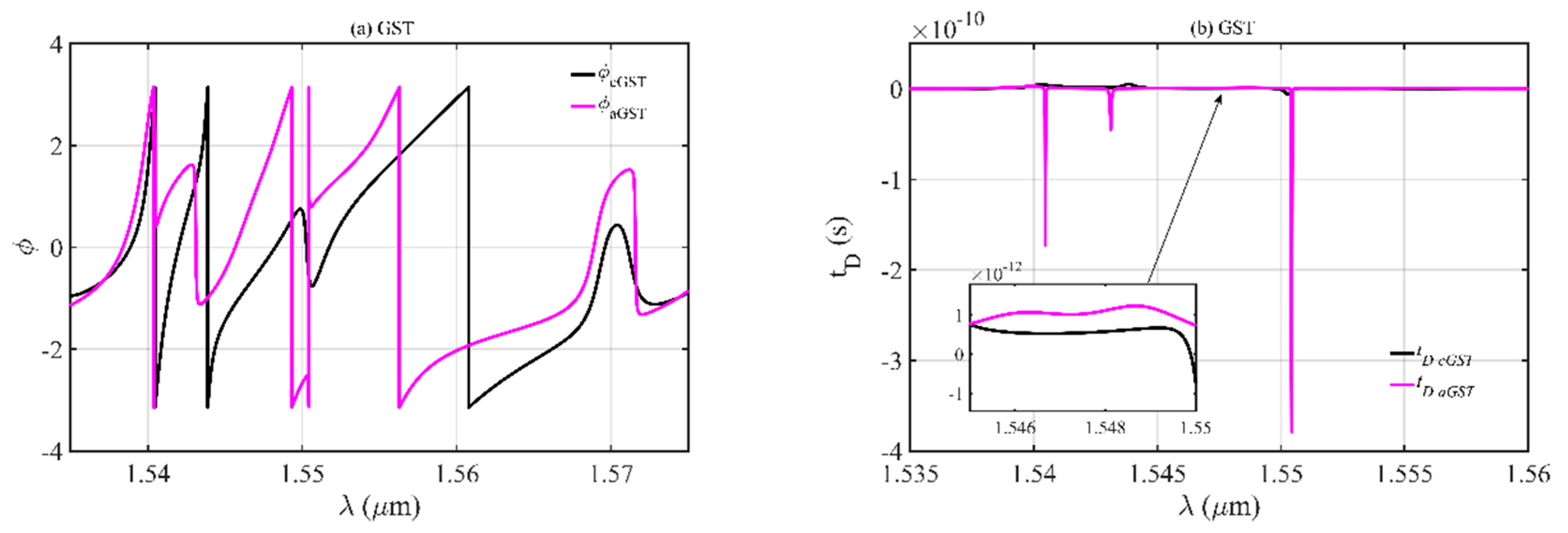
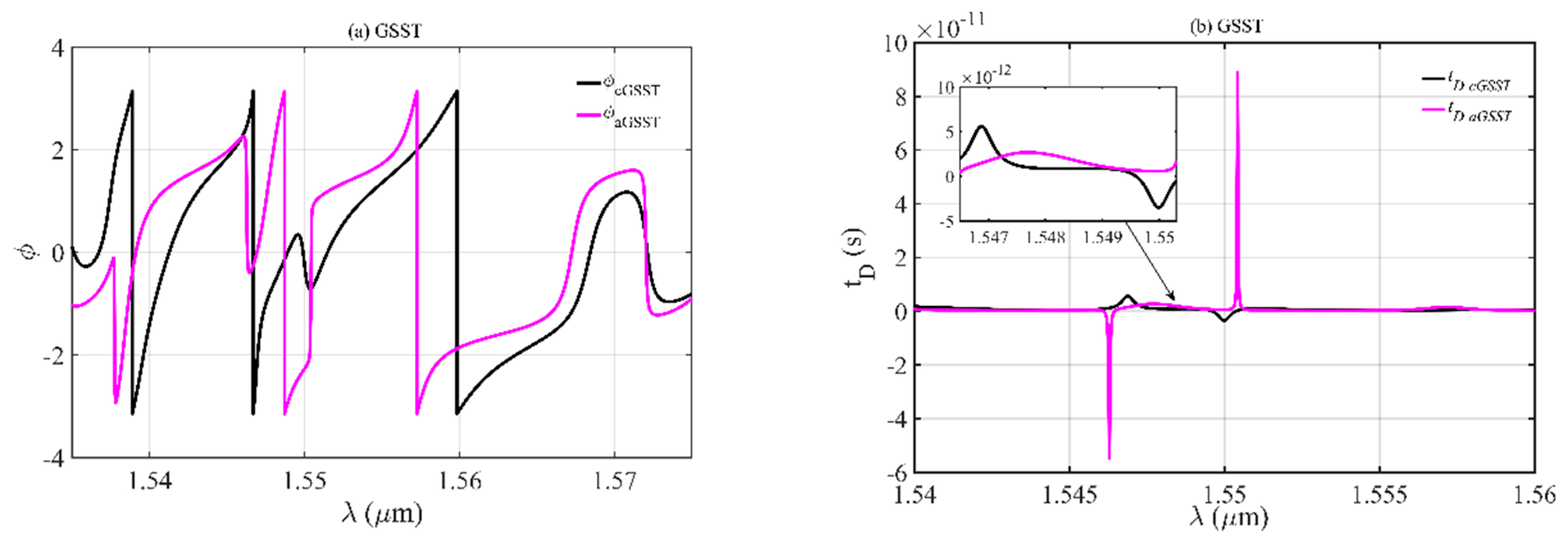
3.2. Write-in Operation and Effective Buffering Time

The optical signal is input from the input port of the Sagnac ring. The initial state of PCM (GST or GSST) is amorphous, and the forward optical signal can be coupled into the micro-ring R3, R2 and R1 in sequence, so that the optical signal can write into the optical buffer. By applying light pulse or electric pulse to the PCM, the phase of the PCM can transition to crystalline, so that R3 and R2 are decoupled, and the light is stored in the MOMR R2 and R1. When the power of the signal light reaches 1/e times of its initial value, the delay time is the effective storage time of the buffer, that is, P o u t ( t ) / P i n ( t ) = 1 / e . Therefore, the delay length of the optical signal in the buffer is L = 1 α ln ( P i n P o u t ) , here α = 4 π k e f f / λ . So, the effective buffering time of the optical buffer is t = L n e f f / c , which is 116.19 ps. The effective refractive index and the extinction coefficient of the double micro-rings (R1 and R2) waveguide are n e f f , S i = 2.2742 and k e f f , Si = 8.0476 × 10 6 .
Figure 7 shows the sum of the transmittance of the output port and the reflectivity of the reflecting port in Sagnac optical buffer based on three MOMRs with GST. The red and blue curves in Figure 7 are the sum of transmittance curve (blue line) and reflectance curve (pink line) in GST amorphous state in Figure 4a and crystalline state in Figure 4b respectively. At the wavelength of 1.55025 μm, the sum of transmittance and reflectance of cGST has a peak value of −27.39 dB, which proves that the signal is stored in the double micro-rings R2 and R1. Meanwhile, the sum of transmittance and reflectance of aGST at this position is −0.43 dB; at that time, the signal is output from the reflecting port of the Sagnac ring.
In the same way, Figure 8 shows the sum of the transmittance of the output port and the reflectivity of the reflecting port in Sagnac optical buffer based on 1 × 3 MOMRs with GSST. The red and blue curves in the figure are the sum of transmittance curve (blue line) and reflectance curve (pink line) in GSST amorphous state in Figure 6a and crystalline state in Figure 6b respectively. At the wavelength of 1.5501 μm, the sum of transmittance and reflectance of cGSST has a peak value of −29.81 dB, which proves that the signal is stored in the double micro-rings R2 and R1. Meanwhile, the sum of transmittance and reflectance of aGSST at this position is −0.03 dB; at that time, the signal is output from the reflecting port of the Sagnac ring.
For the Sagnac ring coupled MOMRs system, the close juxtaposition of absorption lines leads to an optical phase Φ that changes rapidly as a function of frequency in the frequency window between two adjacent absorption lines [14]. Φ(ω) is the accumulated phase. Since the group delay is equal to tD = −/ [30], this leads to a large delay for a pulse whose carrier frequency is centered between lines.
Figure 9 shows phase Φ and group delay tD of the Sagnac ring coupled 1 × 3 MOMRs with GST. As shown in Figure 9b, there are three peaks in the group delay curve of aGST (the pink line), −172.4 ps, −45.01 ps and −378.85 ps, respectively, at the wavelength of 1.5405 μm, 1.5431 μm and 1.5504 μm. The black line is the group delay curve of cGST in the Sagnac ring coupled MOMRs system. It has two peak values: 5.34 ps at the wavelength of 1.5438 μm and −6.11 ps at the wavelength of 1.5503 μm.
Figure 10 shows phase Φ and group delay tD of Sagnac ring coupled 1 × 3 MOMRs with GSST. As shown in Figure 10b, there are two peaks in the group delay curve of aGSST (the pink line): −54.75 ps at the wavelength of 1.5463 μm and 88.92 ps at the wavelength of 1.5504 μm. The black line shows the group delay curve of cGST in the Sagnac ring coupled MOMRs system, and the peak values are 5.59 ps and −3.5 ps, respectively, at the wavelength of 1.5469 μm and 1.5500 μm.
The difference of refractive index between GST and GSST results in the difference of the accumulated phase Φ(ω) in the transmission process when optical signal in R3 ring, that ultimately leads to the difference of the group delay tD in Figure 9b and Figure 10b. This indicates that the optical signal pulse travels at different group velocities in this two types of R3 rings with GST and GSST, since the reciprocal of group delay per unit length is group velocity. As a result of this difference in time delays, the optical signal pulse spreads out with time as it is transmitted over the rings.

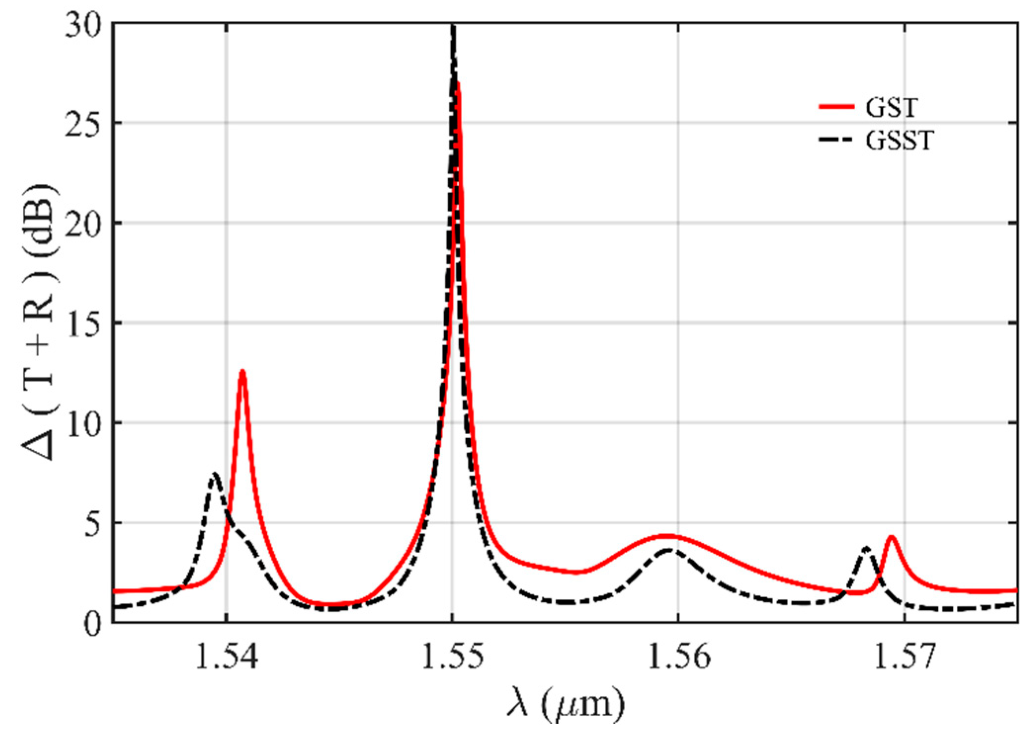
3.3. Read-Out Operation and Performance Comparison

When the optical signal is stored in the optical buffer for a period of time, by applying suitable optically or electrically provided heat stimuli, the PCM is transformed into an amorphous state, which has a lower effective refractive index and extinction coefficient. Therefore, the optical signal can be re-coupled from the micro-rings R2 and R1 into R3, and output from the Sagnac ring, realizing the read-out control of the optical buffer.
A variety of methods has triggered the phase-switching of PCM between the crystalline and amorphous states and the modulation of the optical transmission, including external pulses to heat the PCM by means of heater [31] or pump-probe [32,33,34]. The pump-probe scheme is an on-chip switching technique that allows the operation of all-optical and full integration, which is optimum for integration in the future. Moreover, by applying only a single pulse (light pulse or electric pulse) to the PCM regardless of the previous state of the device, the phase of the PCM can switch its state to either amorphization or crystallization within a few tens of nanoseconds [35,36]. For example, the conversion to an amorphous state was obtained by employing a pump pulse with enough energy to melt-quench the GST rapidly and favor a disordered state [37].
Figure 11 shows the difference of optical buffering between amorphization and crystallization states of PCM (GST and GSST), which is covered on the third MOMR of the optical buffer. The red solid line is the difference between the sum of the transmittance of the output port and the reflectivity of the reflecting port in Sagnac optical buffer with aGST and cGST, that is, the difference between the blue line and the red line in Figure 7. Meanwhile, the black dotted line is the difference between the sum of the transmittance of the output port and the reflectance of the reflecting port in Sagnac optical buffer with aGST (blue line) and cGSST (red line) in Figure 8. This difference value represents the on/off ratio of the optical buffer and indicates the difficulty of switching control. The larger value means greater difference of the storage capacity between the two states of PCM. It can be seen from the Figure 11 that the 3 dB bandwidth of the buffer covered with GST material is 0.176 nm, the product of time-bandwidth can reach 16.04, and the calculated Q factor of the device is 8.819 × 10³. When covering GSST material in the optical buffer, the 3 dB bandwidth is 0.114 nm, the product of time-bandwidth can reach 10.39, and the corresponding Q factor is 1.3652 × 10⁴.
Table 1 summarizes some representative research works of optical buffers based on MR structure over the past 7 years. From the table, it is apparent that silicon-integrated optical buffers have achieved considerable progress in this time. They are approaching sufficient performances that meet practical application needs in C-band wavelength range, which are very promising for next-generation silicon photonic systems. However, increasing buffering time while reducing device size remains a challenge.
The optical buffer in this work has a longer buffering time than the micro-ring buffer of the same device size. It can realize the function of high-precision time delay and meet the requirements of clock alignment accuracy and bandwidth in high-speed optical networks.

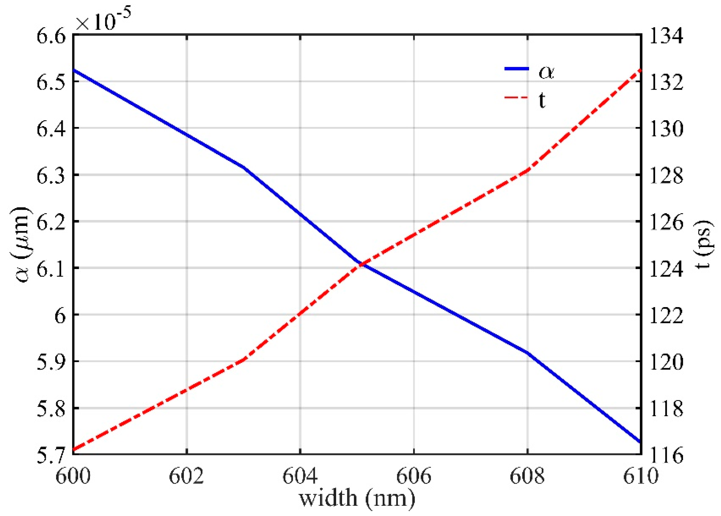
3.4. Tolerance Analysis

In order to discuss the influence of the geometry of micro-rings on the resonant wavelength. We calculated the resonance deviation caused by the difference of the micro-rings radius and the difference of the waveguide width. Figure 12a shows the relationship between the radius difference of the micro-rings and the deviation of the resonant wavelength. It can be seen that the deviation of the resonant wavelength increases linearly with the increase of the radius difference of the micro-rings. The wavelength shift of 3.54 nm can be induced by the change of 10 nm radius. Figure 12b shows the relation between the width difference of the micro-ring waveguides and the deviation of the resonant wavelength. The curve shows that the deviation of the resonant wavelength increases gradually with the increase of the width difference of the micro-ring waveguide, and a wavelength shift of 0.022 nm is induced by a variation in waveguide width of 10 nm.
The width of the micro-ring waveguide affects not only the resonant wavelength, but also the loss coefficient of the waveguide and the effective buffering time. In Figure 13, the blue curve shows the variation of the loss coefficient with the width of the waveguide, and the red curve shows the relationship between the width of the waveguide and the effective buffering time. It can be seen that, with the increase of the micro-ring waveguide width, the loss coefficient decreases and the effective buffering time increases gradually. The red curve shows that increasing the waveguide width of 10 nm can improve the effective buffering time by 16.31 ps.

4. Conclusions

In this study, a SOI MO micro-rings (MOMRs) array coupled with Sagnac ring was studied to realize the function of a switchable optical buffer, which can exceed the time-bandwidth limitation. The transmission equations of the three-ring coupled straight waveguide and three-ring coupled Sagnac ring were derived. The transmission spectra of three MOMRs with GST and GSST in crystalline and amorphous states were calculated. The transmission and reflection spectra, phase and group delay of Sagnac ring coupled three MOMRs based on aGST, cGST, aGSST and cGSST were calculated. The buffering time of the buffer can reach 116.19 ps. A method of switching the state of the PCM (crystalline or amorphous) to implement the writing, storage and reading control of the optical buffer were proposed and discussed. The influence of the geometry of micro-rings on the resonant wavelength and effective buffering time were discussed. The Q factors of optical buffer based on GST or GSST were calculated, which are 8.819 × 10³ and 1.3652 × 10⁴, and the product of time-bandwidth can reach 16.04 and 10.39, respectively.

Author Contributions

Writing—original draft preparation, H.W.; writing—review and editing, Z.W.; visualization, Z.F. and R.J.; supervision, L.L., J.W., C.W. All authors have read and agreed to the published version of the manuscript.

Funding

This work is funded by Beijing Natural Science Foundation (L201021), and National key R & D plan (2021YFB2900700).

Conflicts of Interest

The authors declare no conflict of interest.

References

  1. Wang, Q.; Yu, L.; Gao, H.; Chu, S.; Peng, W. Electromagnetically induced transparency in an all-dielectric nano-metamaterial for slow light application. Opt. Express 2019, 27, 35012–35026. [Google Scholar] [CrossRef] [PubMed]
  2. Keleshtery, M.H. Analysis and investigation of slow light based on plasmonic induced transparency in metal-dielectric-metal ring resonator in a waveguide system with different geometrical designs. Opt. Photonics J. 2016, 6, 177. [Google Scholar] [CrossRef] [Green Version]
  3. Zadok, A.; Eyal, A.; Tur, M. Stimulated Brillouin scattering slow light in optical fibers. Appl. Opt. 2011, 50, E38–E49. [Google Scholar] [CrossRef]
  4. McMillan, J.F.; Yang, X.; Panoiu, N.-C.; Osgood, R.M.; Wong, C.W. Enhanced stimulated Raman scattering in slow-light photonic crystal waveguides. Opt. Lett. 2006, 31, 1235–1237. [Google Scholar] [CrossRef] [PubMed] [Green Version]
  5. Baba, T. Slow light in photonic crystals. Nat. Photonics 2008, 2, 465. [Google Scholar] [CrossRef]
  6. Kassa-Baghdouche, L.; Boumaza, T.; Bouchemat, M. Optimization of Q-factor in nonlinear planar photonic crystal nanocavity incorporating hybrid silicon/polymer material. Phys. Scr. 2015, 90, 065504. [Google Scholar] [CrossRef]
  7. Kassa-Baghdouche, L.; Cassan, E. Mid-infrared refractive index sensing using optimized slotted photonic crystal waveguides. Photonics Nanostruct.-Fundam. Appl. 2018, 28, 32–36. [Google Scholar] [CrossRef]
  8. Elshahat, S.; Abood, I.; Liang, Z.; Pei, J.; Ouyang, Z. Sporadic-Slot Photonic-Crystal Waveguide for All-Optical Buffers with Low-Dispersion, Distortion, and Insertion Loss. IEEE Access 2020, 8, 77689–77700. [Google Scholar] [CrossRef]
  9. Wang, X.; Zhou, L.; Li, R.; Xie, J.; Lu, L.; Wu, K.; Chen, J. Continuously tunable ultra-thin silicon waveguide optical delay line. Optica 2017, 4, 507–515. [Google Scholar] [CrossRef]
  10. Moralis-Pegios, M.; Mourgias-Alexandris, G.; Terzenidis, N.; Cherchi, M.; Harjanne, M.; Aalto, T.; Miliou, A.; Pleros, N.; Vyrsokinos, K. On-chip SOI delay line bank for optical buffers and time slot interchangers. IEEE Photonics Technol. Lett. 2017, 30, 31–34. [Google Scholar] [CrossRef]
  11. Liu, D.; Sun, S.; Yin, X.; Sun, B.; Sun, J.; Liu, Y.; Li, W.; Zhu, N.; Li, M. Large-capacity and low-loss integrated optical buffer. Opt. Express 2019, 27, 11585–11593. [Google Scholar] [CrossRef] [PubMed]
  12. Wang, C.; Liu, X.; Zhang, M.; Zhou, P. Low dispersion broadband integrated double-slot microring resonators optical buffer. Front. Optoelectron. 2016, 9, 571–577. [Google Scholar] [CrossRef]
  13. Liu, W.; Romeira, B.; Li, M.; Guzzon, R.S.; Norberg, E.J.; Parker, J.S.; Coldren, L.A.; Yao, J. A wavelength tunable optical buffer based on self-pulsation in an active microring resonator. J. Lightwave Technol. 2016, 34, 3466–3472. [Google Scholar] [CrossRef]
  14. Kalantarov, D. Tunable low dispersion optical delay line using three coupled micro-resonators. J. Opt. 2017, 19, 115802. [Google Scholar] [CrossRef]
  15. Guo, Z. Photon Storage in a Dynamic Two-Ring-Two-Bus System. Opt. Photonics J. 2019, 9, 20. [Google Scholar] [CrossRef] [Green Version]
  16. Ni, S.; Wu, B.; Liu, Y. Characteristics of silicon-based Sagnac optical switches using magneto-optical micro-ring array. Fiber Integr. Opt. 2018, 37, 12–20. [Google Scholar] [CrossRef]
  17. Fan, L.; Li, Y.; Zhao, W.; Li, J.; Zhang, X.; Peng, C.; Wu, Y.; Zou, M.; Fang, B.; Wang, X. Optical Buffer Device Employing VO2 Embedded on SOI Waveguides With Microring Resonator. IEEE Photonics J. 2021, 13, 1–11. [Google Scholar] [CrossRef]
  18. Kumar, A.; Kumar, M.; Jindal, S.K.; Raghuwanshi, S.K.; Choudhary, R. Implementation of all-optical 1 × 4 memory register unit using the micro-ring resonator structures. Opt. Quantum Electron. 2021, 53, 492. [Google Scholar] [CrossRef]
  19. Tsakmakidis, K.L.; Shen, L.; Schulz, S.A.; Zheng, X.; Upham, J.; Deng, X.; Altug, H.; Vakakis, A.F.; Boyd, R.W. Breaking Lorentz reciprocity to overcome the time-bandwidth limit in physics and engineering. Science 2017, 356, 1260–1264. [Google Scholar] [CrossRef] [Green Version]
  20. Hui-Ying, W.; Zhi, W.; Can, C.; Hang-Tian, L.; Qiang, L.; Xiang-Kong, Z.; Jian, W.; Chong-Qing, W. Dispersion characteristics of nonreciprocal gyroelectric silicon-on-insulator rectangular waveguide. Acta Phys. Sin. 2019, 68. [Google Scholar]
  21. Wang, H.; Wang, Z.; Li, H.; Zhan, X.; Cui, C.; Fu, Z.; Li, Z.; Liu, L.; Wu, C. Signal evolution of an optical buffer based on the nonreciprocal silicon-on-insulator waveguide. Opt. Commun. 2020, 474, 126158. [Google Scholar] [CrossRef]
  22. Cheng, Z.; Ríos, C.; Youngblood, N.; Wright, C.D.; Pernice, W.H.P.; Bhaskaran, H. Device-level photonic memories and logic applications using phase-change materials. Adv. Mater. 2018, 30, 1802435. [Google Scholar] [CrossRef] [PubMed] [Green Version]
  23. Song, J.; Ghosh, S.; Dhingra, N.; Zhang, H.; Zhou, L.; Rahman, B.M.A. Feasibility study of a Ge2Sb2Te5-clad silicon waveguide as a non-volatile optical on-off switch. OSA Contin. 2019, 2, 49–63. [Google Scholar] [CrossRef] [Green Version]
  24. Xu, P.; Zheng, J.; Doylend, J.K.; Majumdar, A. Low-loss and broadband nonvolatile phase-change directional coupler switches. ACS Photonics 2019, 6, 553–557. [Google Scholar] [CrossRef] [Green Version]
  25. Bahlmann, N.; Chandrasekhara, V.; Erdmann, A.; Gerhardt, R.; Hertel, P.; Lehmann, R.; Salz, D.; Schroteler, F.-J.; Wallenhorst, M.; Dotsch, H. Improved design of magnetooptic rib waveguides for optical isolators. J. Lightwave Technol. 1998, 16, 818–823. [Google Scholar] [CrossRef]
  26. Zhou, H.; Chee, J.; Song, J.; Lo, G. Analytical calculation of nonreciprocal phase shifts and comparison analysis of enhanced magneto-optical waveguides on SOI platform. Opt. Express 2012, 20, 8256–8269. [Google Scholar] [CrossRef] [PubMed]
  27. Dötsch, H.; Bahlmann, N.; Zhuromskyy, O.; Hammer, M.; Wilkens, L.; Gerhardt, R.; Hertel, P.; Popkov, A.F. Applications of magneto-optical waveguides in integrated optics: Review. JOSA B 2005, 22, 240–253. [Google Scholar] [CrossRef]
  28. Zhang, H.; Zhou, L.; Xu, J.; Lu, L.; Chen, J.; Rahman, B.M.A. All-optical non-volatile tuning of an AMZI-coupled ring resonator with GST phase-change material. Opt. Lett. 2018, 43, 5539–5542. [Google Scholar] [CrossRef]
  29. Zhang, Y.; Fowler, C.; Liang, J.; Azhar, B.; Shalaginov, M.Y.; Deckoff-Jones, S.; An, S.; Chou, J.B.; Roberts, C.M.; Liberman, V.; et al. Electrically reconfigurable non-volatile metasurface using low-loss optical phase-change material. Nat. Nanotechnol. 2021, 16, 661–666. [Google Scholar] [CrossRef]
  30. Heebner, J.; Grover, R.; Ibrahim, T. Optical Microresonator Theory; Springer: New York, NY, USA, 2008. [Google Scholar]
  31. Kato, K.; Kuwahara, M.; Kawashima, H.; Tsuruoka, T.; Tsuda, H. Current-driven phase-change optical gate switch using indium–tin-oxide heater. Appl. Phys. Express 2017, 10, 072201. [Google Scholar] [CrossRef]
  32. Ríos, C.; Stegmaier, M.; Hosseini, P.; Wang, D.; Scherer, T.; Wright, C.D.; Bhaskaran, H.; Pernice, W.H.P. Integrated all-photonic non-volatile multi-level memory. Nat. Photonics 2015, 9, 725–732. [Google Scholar] [CrossRef] [Green Version]
  33. Ríos, C.; Youngblood, N.; Cheng, Z.; Le Gallo, M.; Pernice, W.H.P.; Wright, C.D.; Sebastian, A.; Bhaskaran, H. In-memory computing on a photonic platform. Sci. Adv. 2019, 5, eaau5759. [Google Scholar] [CrossRef] [PubMed] [Green Version]
  34. Cheng, Z.; Ríos, C.; Pernice, W.H.P.; Wright, C.D.; Bhaskaran, H. On-chip photonic synapse. Sci. Adv. 2017, 3, e1700160. [Google Scholar] [CrossRef] [Green Version]
  35. Li, X.; Youngblood, N.; Ríos, C.; Cheng, Z.; Wright, C.D.; Pernice, W.H.; Bhaskaran, H. Fast and reliable storage using a 5 bit, nonvolatile photonic memory cell. Optica 2019, 6, 1–6. [Google Scholar] [CrossRef]
  36. Stegmaier, M.; Ríos, C.; Bhaskaran, H.; Pernice, W.H.P. Thermo-optical effect in phase-change nanophotonics. Acs Photonics 2016, 3, 828–835. [Google Scholar] [CrossRef]
  37. Fu, Z.; Wang, Z.; Wang, H.; Jiang, R.; Liu, L.; Wu, C.; Wang, J. Thermal dynamics of phase switching process of an SOI rib waveguide covered with a Ge2Sb2Te5 phase change material film. Opt. Mater. 2022, 124, 112046. [Google Scholar] [CrossRef]
Figure 1. (a) Structure of optical buffer based on Sagnac ring coupled 1 × 3 MOMRs; (b) Section diagram of waveguide.
Photonics 09 00366 g001
Figure 2. Coupling of micro-ring array with straight waveguide: (a) Coupling of a single micro-ring with a straight waveguide; (b) Coupling of double micro-rings in series with straight waveguide; (c) Coupling of three micro-rings in series with straight waveguide.
Photonics 09 00366 g002
Figure 3. Transmission spectra of 1 × 3 MOMRs with (a) aGST and (b) cGST.
Photonics 09 00366 g003
Figure 4. Transmission and reflection spectra of Sagnac ring coupled 1 × 3 MOMRs based on (a) aGST, and (b) cGST.
Photonics 09 00366 g004
Figure 5. Transmission spectra of 1 × 3 MOMRs with (a) aGSST and (b) cGSST.
Photonics 09 00366 g005
Figure 6. Transmission and reflection spectra of Sagnac ring coupled 1 × 3 MOMRs based on (a) aGSST and (b) cGSST.
Photonics 09 00366 g006
Figure 7. The sum of the transmittance of the output port and the reflectivity of the reflecting port in Sagnac optical buffer based on 1 × 3 MOMRs with GST.
Photonics 09 00366 g007
Figure 8. The sum of the transmittance of the output port and the reflectivity of the reflecting port in Sagnac optical buffer based on 1 × 3 MOMRs with GSST.
Photonics 09 00366 g008
Figure 9. (a) Phase Φ and (b) group delay tD of Sagnac ring coupled 1 × 3 MOMRs with GST.
Photonics 09 00366 g009
Figure 10. (a) Phase Φ and (b) group delay tD of Sagnac ring coupled 1 × 3 MOMRs with GSST.
Photonics 09 00366 g010
Figure 11. The difference of optical buffering between amorphization and crystallization states of PCM (GST and GSST).
Photonics 09 00366 g011
Figure 12. Resonance wavelength deviation caused by (a) the difference of radius ∆r, and (b) the difference of waveguide width ∆width.
Photonics 09 00366 g012
Figure 13. Curves of waveguide width, loss coefficient and effective buffering time.
Photonics 09 00366 g013
Table 1. Comparison of characteristics of MR structure optical buffers.
Ref.YearDevice TypeWavelength (nm)Buffer Time (ps)SizeExperiment/Simulation
[12]2016SOI15501505.1 × 10−5 mmSimulation
[13]2016InP MZI1558.8251.72 × 105mm dimensionExperiment
[15]2019SOI1532.5620μm dimensionSimulation
[17]2021SOI1553.778.28μm dimensionSimulation
this work2022Si + MO1550116.19μm dimensionSimulation
Publisher’s Note: MDPI stays neutral with regard to jurisdictional claims in published maps and institutional affiliations.

