Communication

The Optimization of Metal Nitride Coupled Plasmon Waveguide Resonance Sensors Using a Genetic Algorithm for Sensing the Thickness and Refractive Index of Diamond-like Carbon Thin Films

by
Jaturong Junrear
,
Panarit Sakunasinha
and
Surasak Chiangga
*
Department of Physics, Faculty of Science, Kasetsart University, Bangkok 10900, Thailand
*
Author to whom correspondence should be addressed.
Photonics 2022, 9(5), 332; https://doi.org/10.3390/photonics9050332
Submission received: 8 March 2022 / Revised: 26 April 2022 / Accepted: 9 May 2022 / Published: 11 May 2022

Abstract

:
We theoretically designed the Kretschmann configuration coupled plasmon-waveguide resonance (CPWR) sensors, composed of thin films of metal nitrides. The thicknesses of the layers of the CPWR sensors were optimized using a genetic algorithm. The optimized CPWR sensors were applied to simultaneously measure the thickness and refractive index (RI) of diamond-like carbon (DLC) films. The field profiles and the sensitivity of the CPWR sensors in response to thin DLC films were studied using the finite-different time-domain technique and the transfer matrix method. The genetic algorithm method predicted that the two-mode CPWR sensors could simultaneously analyze the thickness and RI of the DLC films as thin as 1.0 nm at a wavelength of 1550 nm. The simulations showed that the angular sensitivity toward the refractive index changes of the DLC films of the optimized CPWR sensors was comparable to that of traditional CPWR sensors.

1. Introduction

Surface plasmons are surface electromagnetic waves that propagate along the metal-dielectric interface. The surface plasmon resonance (SPR) occurs when the wave vector of the surface plasmon is matched with the wave vector of the incident light on a prism in the Kretschmann configuration [1]. Surface plasmons are responsible for several fascinating phenomena that have been employed in a variety of applications [2,3]. Recently, SPR techniques have been used for applications such as the perfect absorbers [4,5] and thickness sensors of thin film overlayers on the active surface plasmon layer [6,7,8]. Typical SPR methods for assessing the thickness of thin film include measuring the reflected intensity as a function of wavelength or angle and finding the positions of the reflectivity minimum, which relate to both the refractive index (RI) and the thickness of the thin film to be measured. The traditional SPR sensor consists of a prism with a noble metallic film coating deposited on top, which is adjacent to a dielectric medium, such as air or water. The traditional coupled plasmon-waveguide resonance (CPWR) architecture consists of a waveguide layer on top of the noble metallic film of the traditional SPR structures [9]. Conventional CPWR sensors have narrow full width at haft maximum and sharp waveguide resonance, and they can be excited by both transverse magnetic (TM) and transverse electric (TE) polarized light [10]. Due to the greater containment of surface plasmons in the waveguides, conventional CPWR sensors have potential advantages over traditional SPR sensors [11]. The CPWR sensors have been used in a range of applications, including chemical and biological sensing [12,13,14], as well as thickness and refractive index (RI) change detection [15,16,17,18]. The traditional CPWR and SPR devices create broad resonances at near-infrared (NIR) wavelengths due to the high ohmic loss of the noble metal films, limiting their usage at these wavelengths [19]. Moreover, the noble metal films have a low damage threshold and lack of compatibility with standard complementary metal oxide semiconductor (CMOS) technology [20]. Thus, the alternative plasmonic materials have been developed to overcome these drawbacks [21,22,23,24,25].
Thin films of titanium nitride (TiN), the alternative plasmonic material, have attracted significant interest for plasmonic applications in recent years due to their plasmonic properties, which are comparable to thin films of gold in the wavelength range of more than 500 nm [26,27,28], and their compatibility with the CMOS fabrication technique [29]. Moreover, the TiN films have tunable optical properties and can resist higher temperatures than gold films [30]. Although thin films of TiN have promised plasmonic performance, there have been few studies on their application in SPR sensors. Some of these studies included numerical investigation of the sensitivity of the TiN/sapphire SPR sensors [31], TiN-coated photonic crystal fiber sensor [32] and experimental demonstration of the responses of sapphire/TiN sensors [33], and fluorescence sensing [34].
To obtain the best performance, the sensitivity and the RI resolution of the SPR sensors were optimized using many optimization techniques including the particle swarm optimization [35,36] and genetic algorithms (GA) [37,38,39]. Although the GA was utilized to optimize the wavelength of the operation and layer thicknesses of the CPWR sensors for biochemical sensing, the waveguide supported only a single resonance for TE and TM modes. The layer structures of the CPWR sensors that can generate multi-resonance dips were not optimized for optimal response.
The objective of this paper was to design the CPWR sensors, which consisted of thin films of TiN and aluminum nitride (AlN), to measure simultaneously the thickness and RI of the diamond-like carbon (DLC) thin films in the NIR spectral range. The DLC thin films were chosen as an example for simultaneously determining thickness and RI because they are extensively used in many industrial applications [40] and they can be grown on the AlN layer without causing any structural changes [41]. To achieve the aim, the CPWR sensors composed of the TiN and AlN layers were designed and optimized to produce either two or three TM resonance minima at a wavelength of 1550 nm using the GA method. The plasmonic response and electrical field profiles of the CPWR structures were investigated using the transfer matrix method (TMM) and a finite-different time-domain (FDTD) technique for the different thicknesses of the DLC thin films. The FDTD technique was utilized to simulate the optical effects of a variety of nanophotonic devices. It has been shown that the FDTD technique allows efficient and precise simulations of spectral responses in plasmonic systems [42,43].

2. Materials and Methods

The design of the CPWR sensors is discussed first, followed by the theoretical models used to analyze them.

2.1. Selection of Materials for CPWR Sensor

Our design was based on the optical loss resulting from the intraband transitions in the NIR spectral range and the compatibility with CMOS fabrication processes of TiN films. To obtain the best plasmonic performance and sensor efficiency, TiN films require suitable substrates and must be integrated with III-V nitrides, such as AlN and GaN, with smooth interfaces and surfaces. Previous studies have shown that TiN thin films can be fabricated on c-sapphire, magnesium oxide (MgO), and silicon substrates. Previous research has also shown that TiN films grown on sapphire substrates had better plasmonic performance than TiN films grown on silica glass or silicon substrates [44,45]. In this work, we examined the CPWR sensors on sapphire, magnesium oxide, and silicon prisms. We focused on the lattice match with TiN while choosing the III-V nitrides as a waveguide. The AlN film, having a lattice constant of 4.08 Å, was chosen because of the low lattice mismatch with TiN, having a lattice constant of 4.24 Å [46]. Moreover, experiments revealed the good adhesion property of the TiN/AlN bilayers [47,48].
Figure 1 shows a schematic representation of the CPWR structures to be studied without and with a thin DLC layer. The CPWR sensor consisted of a prism that was deposited with TiN, and an AlN layer was coated on top of the TiN layer (Figure 1a). A thin DLC film to be evaluated for RI and thickness was deposited on the AlN layer (Figure 1b). The SPR effect is observed when the wave vector of the surface plasmon (ksp) is matched with the wave vector of the incident light (kx,TM) on the prism. The CPWR sensors were in the ambient air.

2.2. Theoretical Modeling

2.2.1. Transfer Matrix Method (TMM)

The Fresnel’s equations and the TMM were used to describe the reflectivity as a function of the angle of incidence of the CPWR structures. The theoretical reflectivity spectra of the CPWR structures were calculated using the MATLAB program. The CPWR system can be modeled as a four-phase model: prism/TiN/AlN/air. Although the CPWR systems can support both TE and TM modes, the SPP can only be created by the TM mode. The details of the TMM method are given in the literature [9,49]. Below, we briefly describe the TMM approach for the CPWR system.
Consider the stack of layers in z-axis direction in the CPWR system, as shown in Figure 1b. The prism and the surrounding medium (air) are numbered 1 and 4, respectively. The films are numbered from 2 to 3, while the interfaces are numbered from 1 to 3. The first interface between the prism and TiN was defined as z = z 1 = 0 , and the plane of incident light as the xz plane. The amplitudes of the electric and magnetic fields, E and H, in the first layer, resulting from the Jth layer, are calculated by multiplying each of the matrices for separate layers as follows [49]:
[ H 1 E 1 ] = j = 1 J 1 M j · [ H j E j ]
The matrix Mj is given by
M j = [ cos ϕ j i sin ϕ j / q j i q j sin ϕ j cos ϕ j ]
where ϕ j is the phase factor in the Jth layer, which can be calculated by
ϕ j = ( 2 π / λ ) ( n j i k j ) d j cos θ j
where λ is the wavelength of the incident light, n j and k j are the refractive index and extinction coefficient of the Jth layer, d j = z j z j 1 is the thickness for the Jth layer, and θ j is the incident angle of the Jth layer, respectively, and
q j = ( μ j / ε j ) 1 / 2 cos θ j
The reflectance of the CPWR system is calculated by
R = | ( m 11 + m 12 q N ) q 1 ( m 21 + m 22 q N ) ( m 11 + m 12 q N ) q 1 + ( m 21 + m 22 q N ) | 2
where q 1 and q N are calculated from Equation (4). For SPR sensors without a DLC coating layer on the TiN layer, q N = q 3 ; for CPWR sensors without a DLC deposition layer on the AlN layer, q N = q 4 ; and for CPWR sensors with a DLC deposition layer on the AlN layer, q N = q 5 .

2.2.2. Drude–Lorentz Model

The dielectric permittivity of the TiN films in the wavelength range of 500–2000 nm were obtained by fitting the experimentally measured spectroscopic ellipsometer curve to the Drude–Lorentz model [29]:
ε ( ω ) = ε ω p 2 ω 2 + i Γ D ω + j = 1 3 ω L , j 2 ω 0 , j 2 ω 2 i γ j ω
where ε is the high-frequency dielectric constant, ω p and Γ D are the plasma frequency and Drude damping constant, respectively. ω L , j 2 = f j ω 0 , j γ j , where f j , ω 0 , j and γ j describe the Lorentz oscillator strength, resonant energy, and damping factor, respectively.
The permittivity of TiN films is derived from fitting one Drude and one Lorentz term using a nonlinear least-squares method with ε = 4.7988 , ω p = 7.7557 , Γ D = 0.15586 , ω L = 5.3154 , ω 0 = 3.9169 , and γ = 1.7222 .

2.3. The Finite-Difference Time-Domain (FDTD) Method

Numerical simulations were conducted using the two-dimensional FDTD method with the program OptiFDTD [50]. In the FDTD simulations, the CPWR structures, covering a region of 6 μm × 6 μm, were calculated under the incident plane wave with perfectly matched layers and a two-dimensional cell size of 3 nm. For all simulations, the wavelength was fixed at 1550 nm. The model parameters for the CPWR configurations are summarized in Table 1.

2.4. Genetic Algorithm Optimization

To optimize the CPWR structures, the GA in MATLAB combined with the TMM approach was implemented. We began the algorithms by creating an initial population size of 50 solutions and then running these solutions through a Fitness Function (FF) that was given by:
FF = min(1/(o2 − o1))
where o2 and o1 were the reflection minima of the TM response at the higher and lower resonance angles, respectively.
The constraints were determined by the number of reflection minima (peak): peak ≤ 2, and by the sum of values of reflectivity of the waveguide resonance: Rmax1 + Rmin1 ≥ 0.9. Other parameters used were exponential scaling, randomizing mutation, and one-point crossover. For two reflection minima, the thicknesses of the TiN and AlN films were assumed to be variable in the range of [10, 100] nm and [1300, 5000] nm, respectively.

3. Results

3.1. The Results from the GA Approach

Table 2 shows the results of utilizing the GA technique to predict the optimum TiN and AlN film thicknesses for three CPWR structures with air as the surrounding medium. From the results, the TiN film thickness for the magnesium oxide prism/TiN/AlN/air and silicon prism/TiN/AlN/air sensors was the same, which is a little thinner than the sapphire prism/TiN/AlN/air structure. For the silicon prism/TiN/AlN/air sensors, the GA method predicted that the thickness of the AlN layer was thinner than the sapphire prism/TiN/AlN/air and the magnesium oxide prism/TiN/AlN/air structures. The next part discusses the reflectivity curves as well as the TM and TE modes generated in the waveguides for the three structures.

3.2. Theoretical CPWR Spectra

Figure 2 shows the reflectivity curves as a function of incident angle for the three GA optimized CPWR structures in the ambient air. The reflectivity from the sapphire prism/29.42 nm TiN/ 909.83 nm AlN/air sensor displayed two minima for TM polarized incident light (35.91° and 76.50°) and a single minimum for TE-polarized incident light (56.97°). The reflectivity minima at the incident angles of 35.91° and 76.50° correspond to the waveguide resonance and the SPR, respectively. The reflectivity from the magnesium oxide prism/28.33 nm TiN/ 909.50 nm AlN/air sensor exhibited two minima for TM-polarized incident light (36.72° and 80.91°) and a single minimum for TE-polarized incident light (58.77°). The 36.72° and 80.91° minima correspond to the waveguide resonance and the SPR angles, respectively. The reflectivity from the silicon prism/28.33 nm TiN/ 711.88 nm AlN/air sensor showed two minima for TM-polarized incident light (25.02° and 36.99°) and two minimum for TE-polarized incident light (19.35° and 31.77°). The 25.02° and 36.99° minima correspond to the waveguide resonance and SPR angles, respectively.

3.3. Field Distribution for TM Polarized Light and Penetration Depth

The field intensity relative to the incident field ( | E x | 2 / | E x i n c | 2 ) for three optimized CPWR structures was simulated using the incident angles that correspond to the reflectivity minima (Figure 3). For an AlN thickness of 909.83 nm, the field profiles of the optimized sapphire prism/TiN/AlN/air sensor and magnesium oxide prism/TiN/AlN/air sensor were identical. At the SPR angles, the fields were enhanced by about 40-fold (Figure 3a) and 70-fold (Figure 3b) relative to the incident field for the optimized sapphire prism/TiN/AlN/air and magnesium oxide prism/TiN/AlN/air sensors, respectively. For the silicon prism/TiN/AlN/air sensor, the field at the prism/TiN interface increased as the usual surface plasmon field, which was only enhanced by about 5-fold, and there was a TM 3 mode in the AlN waveguide layer (Figure 3c).
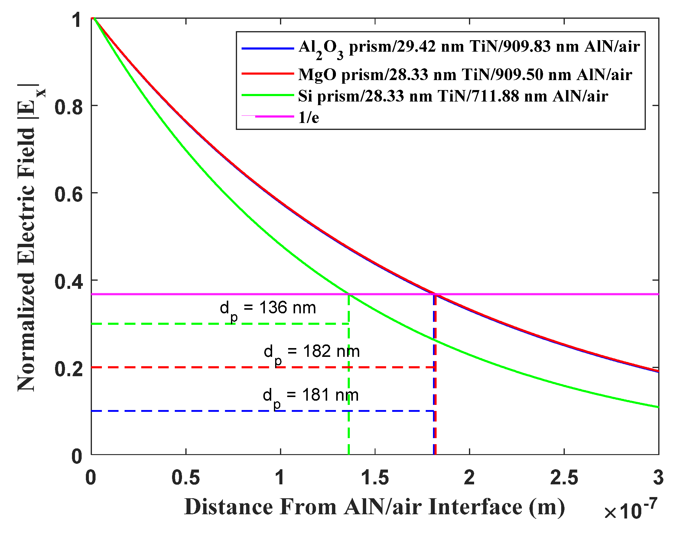
An important parameter when working at a wavelength of 1500 nm is the penetration depth, which quantifies the extent of light penetration into the analyte medium, where the absolute value of the x component of the electric field (|Ex|) decays by factor of 1/e [55,56]. Figure 4 shows the calculated penetration depths at a wavelength of 1500 nm for TM–polarized incident light for each GA–optimized CPWR sensor. The penetration depth of the sapphire prism/TiN/AlN/air sensor was nearly equal to that of the magnesium oxide prism/TiN/AlN/air sensor and slightly higher than that of the silicon prism/TiN/AlN/air sensor.

3.4. Field Distribution for TE Polarized Light

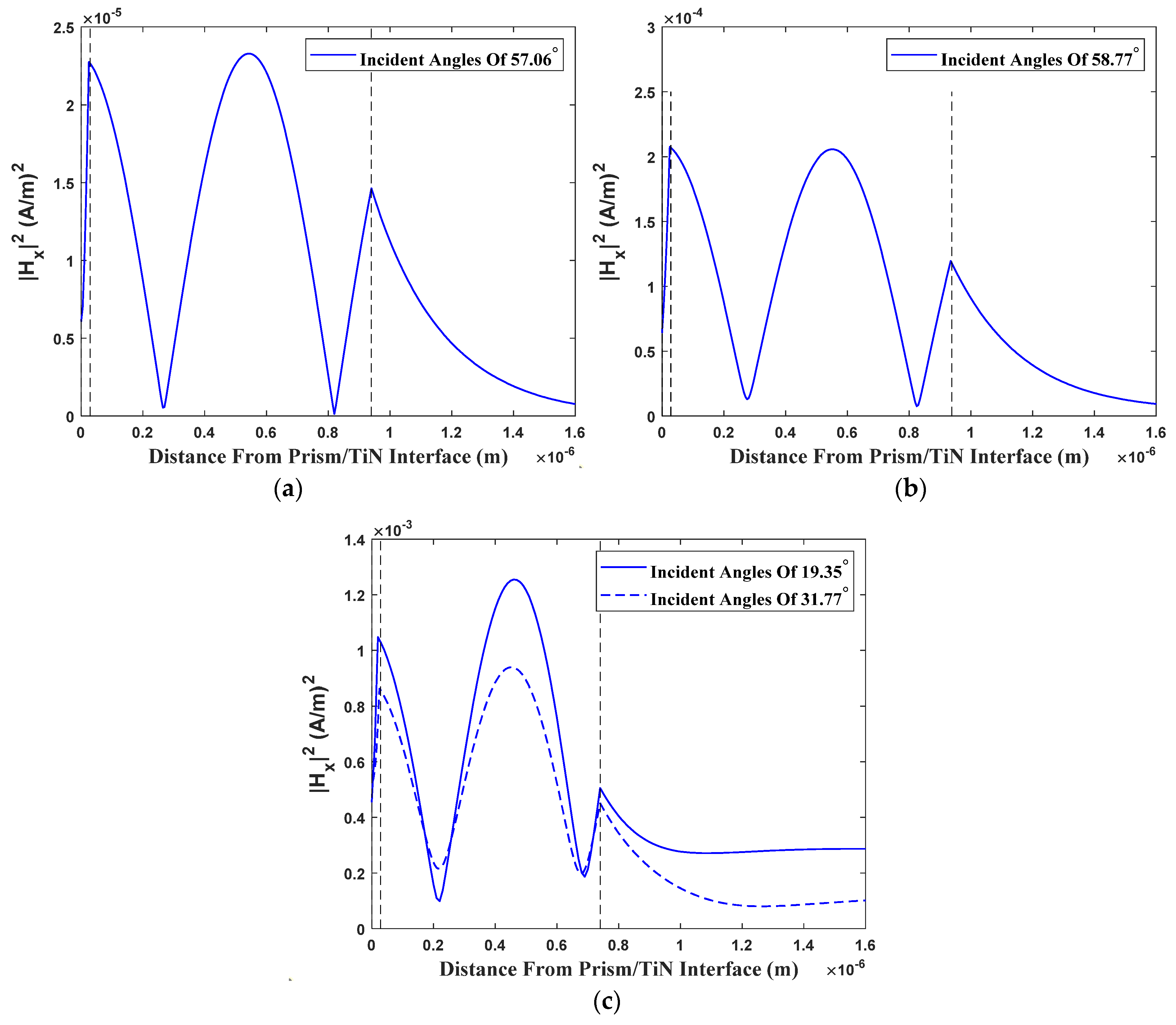
The TE–polarized incident light is also beneficial since the TE modes may provide information about the anisotropy in ultrathin films. The detailed descriptions and examples for lipid orientation determination can be found in [57]. Figure 5 shows the magnetic field distribution for TE modes in the AlN layer for the optimized CPWR sensors. The TE modes in the AlN waveguides were the same for these three sensors. For the sapphire prism/TiN/AlN/air and magnesium oxide prism/TiN/AlN/air sensors, the magnetic fields were increased by around 23-fold and 20-fold, respectively, in comparison to the incident field. For the silicon prism/TiN/AlN/air sensor, the field enhancement factor was lower as compared with the sapphire prism/TiN/AlN/air and magnesium oxide prism/TiN/AlN/air sensors. However, the field was distributed at a distance beyond the AlN/air interface, which could adequately detect the DLC film deposited on top of the AlN layer.

3.5. The Optimized CPWR Sensors Responds to the DLC Film Thicknesses

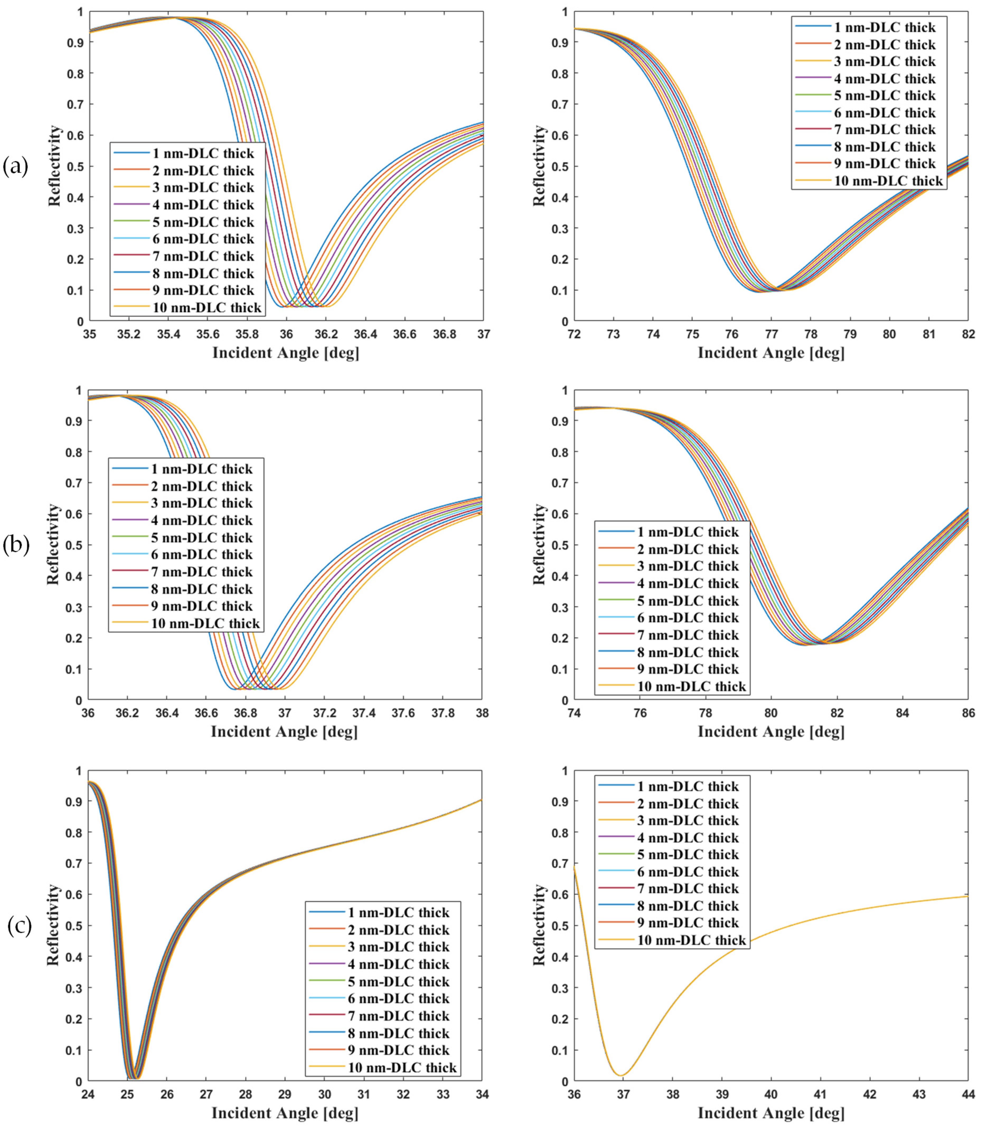
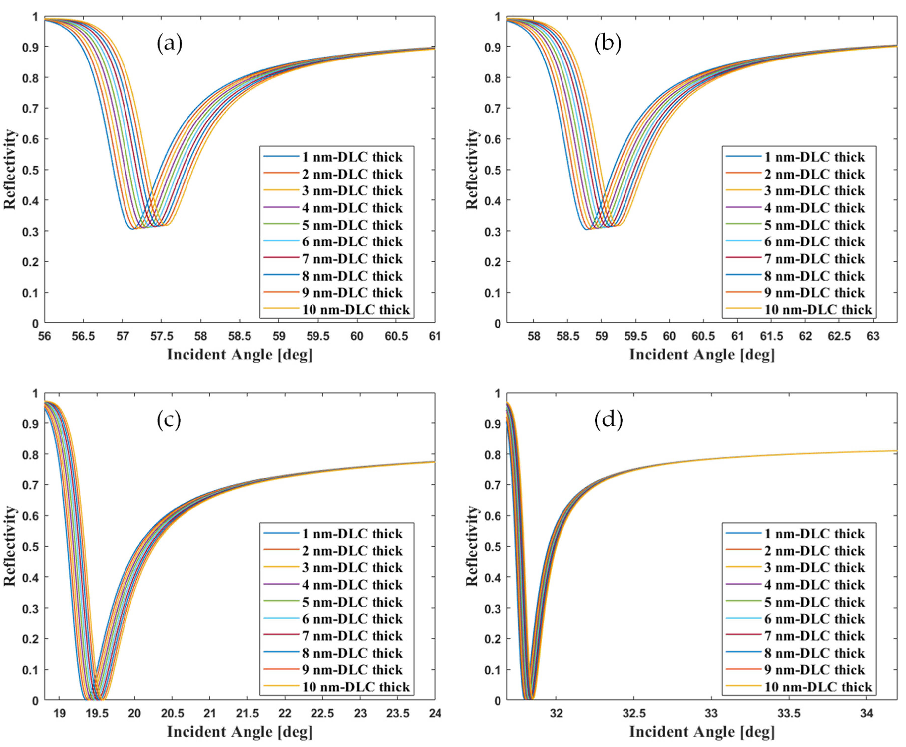
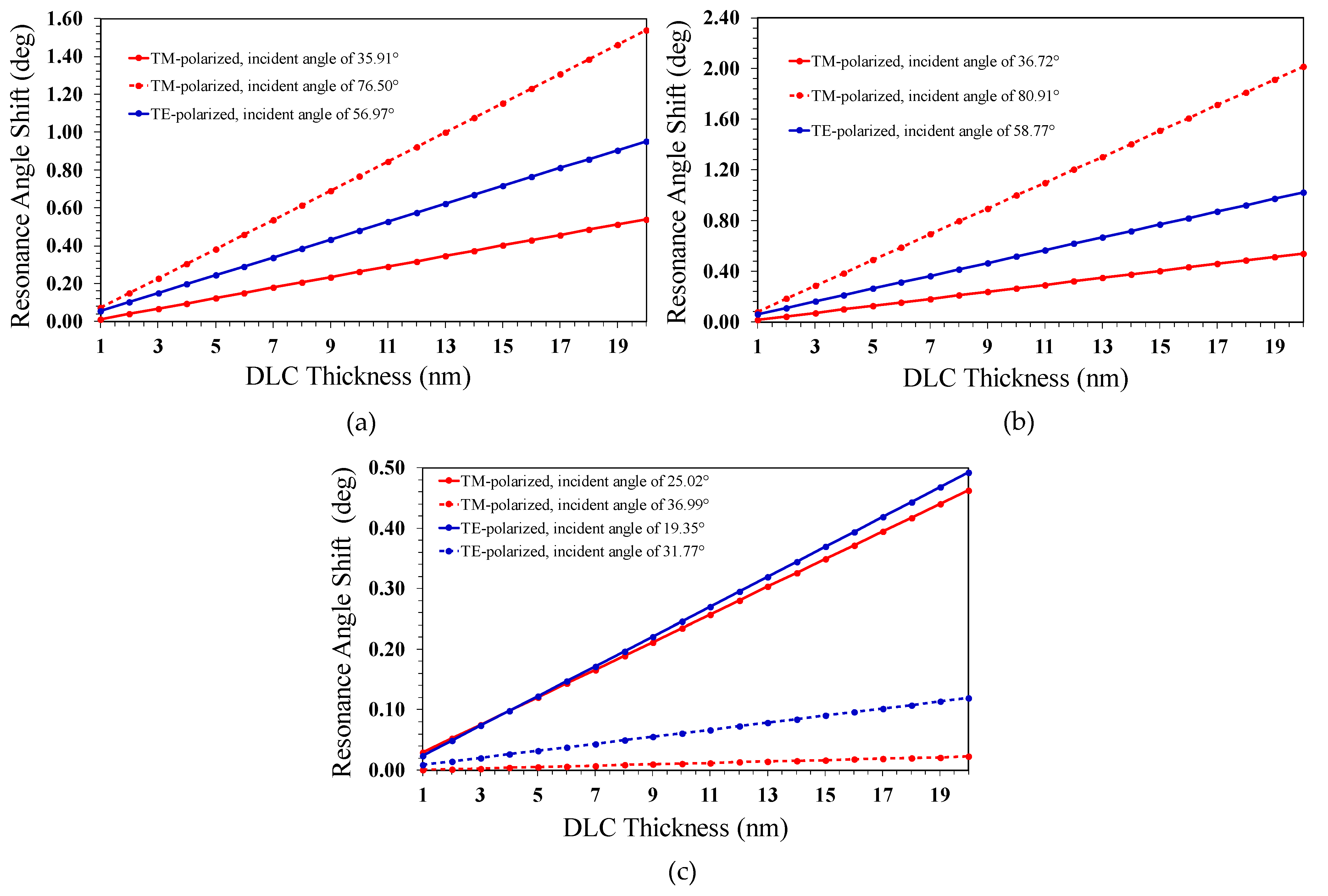
We calculated the reflectivity spectra of the optimized CPWR sensors for TM-polarized (Figure 6) and TE-polarized incident light (Figure 7) to respond to the deposition of the DLC films. With increasing DLC film thickness from 1 to 10 nm in steps of 1 nm, the resonance angles for the TM and TE polarizations shifted to higher angles. Evidently, the silicon prism/TiN/AlN sensor was less sensitive to the DLC film deposited on top of the AlN layer. The thickness sensitivity of a sensor is defined as the ratio of the shift in the resonance angle Δθ to the variation in the thickness of a coating layer Δd. The sensitivities for all optimized CPWR sensors are shown in Figure 8. The shifts in resonance angle curves used for the thickness sensitivity calculation were taken from Figure 6 and Figure 7. The curves were linearly fitted with an average R-square of 0.9995. For TM-polarized incident light of 35.91° and 76.50°, the thickness sensitivity was 0.026 and 0.101, respectively, for the sapphire prism/TiN/AlN/air sensor (Figure 8a). For TM-polarized incident light of 36.72° and 80.91°, the thickness sensitivity was 0.019 and 0.143, respectively, for magnesium oxide prism/TiN/AlN/air sensor (Figure 8b). For TM-polarized incident light of 25.02° and 36.99°, the thickness sensitivity was 0.029 and 0.002, respectively, for silicon prism/TiN/AlN/air sensor (Figure 8c).
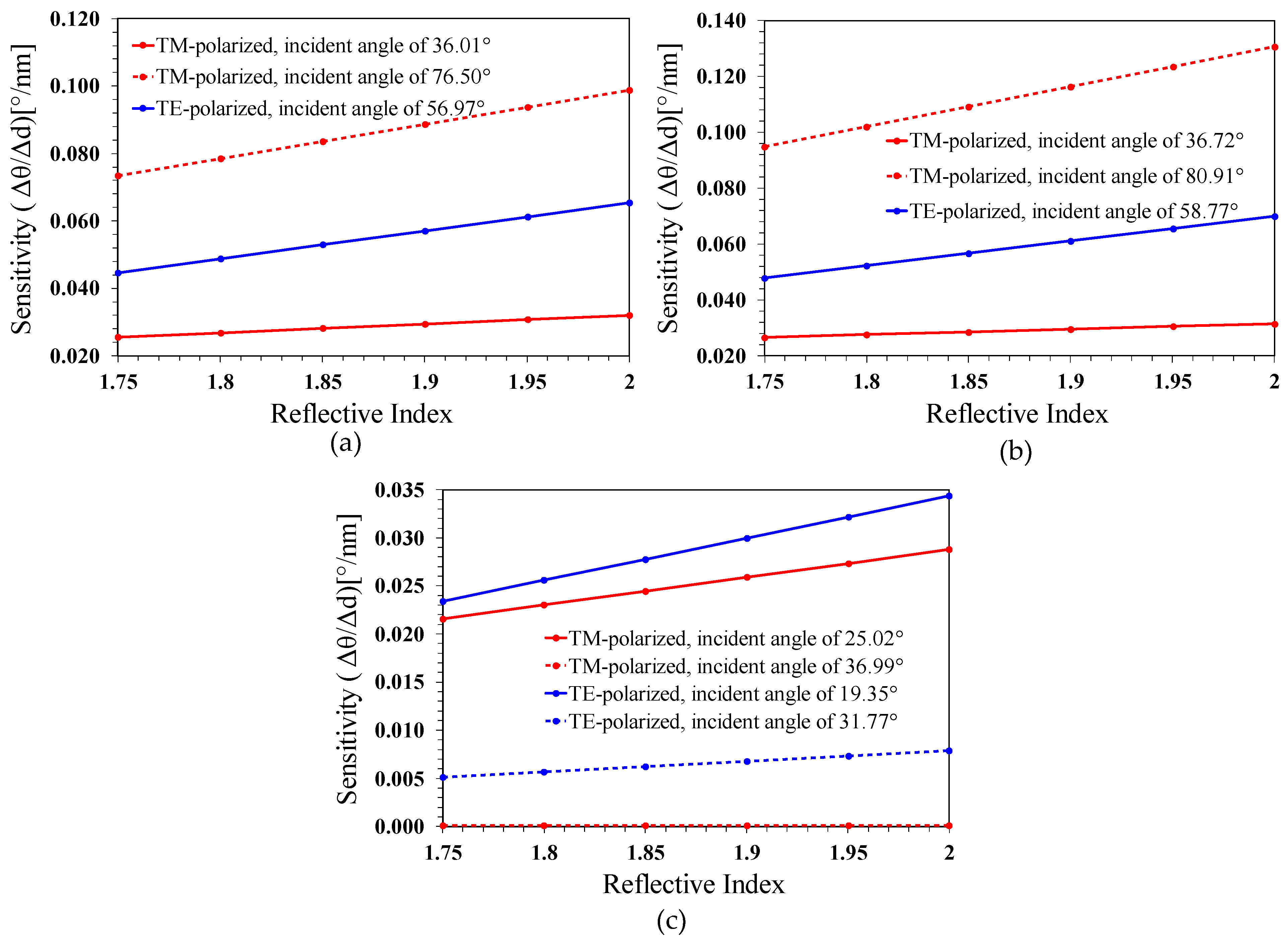
Figure 9 shows the calculated sensitivities for the optimized CPWR sensors as a function of the RI of the thin DLC films and clearly displays the increase linearly in sensitivity towards RI changes of the DLC film. The magnesium oxide prism/TiN/AlN sensor had the highest sensitivity compared to the sapphire prism/TiN/AlN and silicon prism/TiN/AlN sensors. The sensitivity of the SPR at an incident angle of 36.99° for the silicon prism/TiN/AlN sensors was nearly zero. We noted that the optimized sapphire prism/TiN/AlN sensor had a sensitivity comparable to the sensitivity of gold and silica dielectric-loaded waveguide spectroscopy [10].

3.6. Example for Simultaneous Measuring the Thickness and Refractive Index of the DLC Film Using the GA Optimized Sapphire Prism/TiN/AlN/Air Sensor

To get a sense of the experimental use of the optimized CPWR sensors to simultaneously measure the thickness and RI of DLC films, we showed how to extract the thickness and RI of thin DLC films using the graphical technique for the sapphire prism/29.42 nm TiN/909.83 nm AlN sensor (Figure 10). Two trial curves were created for two reflectivity minima for TM-polarized incident light (35.91° and 76.50° in Figure 2). One trial curve (dash) was created at the waveguide resonance angle (at 35.91°) using seven indices of refraction ranging from 1.74 to 1.89. Another trial curve (solid) was created at the surface plasmon resonance angle (at 76.50°) using seven indices of refraction ranging from 1.68 to 1.94. The intersection point of the trial curves was the unique solution for the DLC film thickness and the refractive index. For our example, the intersection point in Figure 10 was (9.14, 1.79), indicating that the thickness and the refractive index for the DLC film were 9.14 nm and 1.79, respectively.

4. Discussion

Many techniques, such as SPR and ellipsometry (SE), require at least two independent measurements to calculate the thickness and RI of thin films simultaneously. The two-color [58], multi-wavelength [59], two-medium [60], and two-thickness [61] techniques are all examples of SPR applications. The drawback of the two-color method, which used two colors of a light source, is that the dispersion function of the thin films must be known. The two-medium approach, using two different external mediums, involves the constraint that the thin films being measured have no interaction with the media. The disadvantage of the two-thickness technique is that prior information about the nominal thickness ratio of the two thin films must be available. In practice, the thickness and RI of thin films have been widely determined using the SE. The disadvantage of SE is that it is expensive and needs the use of elaborate theoretical models for data analysis [62]. Moreover, the SE has proven difficult to determine the thickness and RI of thin films with a thickness of less than 15 nm [63]. Table 3 summarizes the advantages and disadvantages of the two-resonance minima method provided in this work in comparison to previous approaches.
We note that the two reflection minima for the silicon prism/TiN/AlN/air sensor had significantly different sensitivity to the DLC film deposited on top of the AlN layer. As a result, the silicon prism/TiN/AlN/air may be used for self-reference dual-mode thickness sensors [69].
Although the field distribution, penetration depth, and sensitivity of the designed sensors for the magnesium oxide prism were larger than those for the sapphire prism, the sapphires were important for producing optoelectronic devices.
Recent research has explored replacing noble metallic films in sensors based on SPR with alternative plasmonic materials having a high damage threshold and compatibility with standard CMOS technology. This may produce a low-cost, easy-to-use, and CMOS-compatible fabrication process for sensors. Furthermore, sensors that work in the NIR spectral range are important since lasers and detectors are cheap and easily available. Our work on the development of the CPWR sensors made of alternative materials in the NIR wavelength range would allow the further adoption of this class of materials and enable new sensing applications.

5. Conclusions

The designs of CPWR sensors composed of titanium nitride and aluminum nitride thin films for simultaneous thickness and RI measurements of DLC thin films in air at a wavelength of 1550 nm were explored. We optimized the design of CPWR sensors using the genetic algorithm. We examined the responses of the optimized CPWR sensors to the changes in reflectivity curves when the DLC thin films were deposited on top of the CPWR sensors. Furthermore, we simulated the electromagnetic field profiles using the TMM and the FDTD method to understand the coupling between photons and SPPs.
From the simulation results, we concluded that the optimized CPWR sensor could simultaneously characterize the thickness and the refractive index of the DLC films with a minimum thickness of 1.0 nm. The sensitivity of the optimized CPWR sensor was equivalent to that of the conventional CPWR devices. The experimental tests are needed to verify our design and optimization of the CPWR sensors. The design and optimization methods used in this study should be broadly applicable across other plasmon-waveguide resonance sensors.

Author Contributions

Conceptualization, S.C.; investigation, J.J. and P.S.; software, P.S.; analyzed the results, J.J., P.S. and S.C.; writing—original draft preparation, review, and editing, S.C. All authors have read and agreed to the published version of the manuscript.

Funding

This research received no external funding.

Institutional Review Board Statement

Not applicable.

Informed Consent Statement

Not applicable.

Conflicts of Interest

The authors declare no conflict of interest.

References

  1. Raether, H. Surface Plasmons on Smooth and Rough Surfaces and on Gratings; Springer: New York, NY, USA, 2014; ISBN 9783662151235. [Google Scholar]
  2. Kravets, V.G.; Kabashin, A.V.; Barnes, W.L.; Grigorenko, A.N. Plasmonic Surface Lattice Resonances: A Review of Properties and Applications. Chem. Rev. 2018, 118, 5912–5951. [Google Scholar] [CrossRef] [PubMed]
  3. Yesudasu, V.; Pradhan, H.S.; Pandya, R.J. Recent Progress in Surface Plasmon Resonance Based Sensors: A Comprehensive Review. Heliyon 2021, 7, e06321. [Google Scholar] [CrossRef] [PubMed]
  4. Wu, X.; Zheng, Y.; Luo, Y.; Zhang, J.; Yi, Z.; Wu, X.; Cheng, S.; Yang, W.; Yu, Y.; Wu, P. A Four-Band and Polarization-Independent BDS-Based Tunable Absorber with High Refractive Index Sensitivity. Phys. Chem. Chem. Phys. 2021, 23, 26864–26873. [Google Scholar] [CrossRef] [PubMed]
  5. Chen, H.; Chen, Z.; Yang, H.; Wen, L.; Yi, Z.; Zhou, Z.; Dai, B.; Zhang, J.; Wu, X.; Wu, P. Multi-mode surface plasmon resonance absorber based on dart-type single-layer graphene. RSC Adv. 2022, 12, 7821–7829. [Google Scholar] [CrossRef]
  6. Yin, H.; Chen, S.; Huang, R.; Chang, H.; Liu, J.; Qi, W.; He, Z.; Su, R. Real-Time Thickness Measurement of Marine Oil Spill by Fiber-Optic Surface Plasmon Resonance Sensors. Front. Mar. Sci. 2022, 8, 764970. [Google Scholar] [CrossRef]
  7. Andam, N.; Refki, S.; Hayashi, S.; Sekkat, Z. Plasmonic mode coupling and thin film sensing in metal–insulator–metal structures. Sci. Rep. 2021, 11, 15093. [Google Scholar] [CrossRef]
  8. Guo, J.; Zhang, X.; Tian, J.; Zhu, W.; Song, J.; Xiao, H. Evaluating the Refractive Index, Thickness and Porosity of Ultrathin Cellulose Nanocrystal Films with Different Polymorphs by SPR Technique. Int. J. Biol. Macromol. 2021, 193, 1209–1214. [Google Scholar] [CrossRef]
  9. Salamon, Z.; Macleod, H.A.; Tollin, G. Coupled Plasmon-Waveguide Resonators: A New Spectroscopic Tool for Probing Proteolipid Film Structure and Properties. Biophys. J. 1997, 73, 2791–2797. [Google Scholar] [CrossRef] [Green Version]
  10. Hayashi, S.; Nesterenko, D.V.; Sekkat, Z.; Inoue, Y.; Kawata, S. Sharp Resonances in Waveguide-Coupled Surface Plasmon Sensors for Super-Resolution Sensing. In Proceedings of the JSAP-OSA Joint Symposia 2014 Abstracts; OSA: Washington, DC, USA, 2014. [Google Scholar]
  11. Jiang, X.D.; Xu, W.R.; Ilyas, N.; Li, M.C.; Guo, R.K.; Khan, R.; Li, W.; Wang, J.M. High-performance coupled plasmon waveguide resonance optical sensor based on SiO2:Ag film. Results Phys. 2021, 26, 104308. [Google Scholar] [CrossRef]
  12. Convert, L.; Chabot, V.; Zermatten, P.-J.; Hamel, R., Jr.; Cloarec, J.-P.; Lecomte, R.; Aimez, V.; Charette, P.G. Passivation of KMPR Microfluidic Channels with Bovine Serum Albumin (BSA) for Improved Hemocompatibility Characterized with Metal-Clad Waveguides. Sens. Actuators B Chem. 2012, 173, 447–454. [Google Scholar] [CrossRef] [Green Version]
  13. Zourob, M.; Goddard, N.J. Metal Clad Leaky Waveguides for Chemical and Biosensing Applications. Biosens. Bioelectron. 2005, 20, 1718–1727. [Google Scholar] [CrossRef] [PubMed]
  14. Gupta, R.; Goddard, N.J. Leaky Waveguides (LWs) for Chemical and Biological Sensing−A Review and Future Perspective. Sens. Actuators B Chem. 2020, 322, 128628. [Google Scholar] [CrossRef]
  15. Harte, E.; Alves, I.D.; Ihrke, I.; Elezgaray, J. Thickness determination in anisotropic media with plasmon waveguide resonance imaging. Opt. Express 2019, 27, 3264–3275. [Google Scholar] [CrossRef] [PubMed]
  16. Yang, Q.; Gao, L.; Zou, C.; Xie, W.; Tian, C.; Wang, Z.; Liang, F.; Ke, Y.; Zhou, X.; Li, S. Differential Refractive Index Sensor Based on Coupled Plasmon Waveguide Resonance in the C-Band. Sensors 2021, 21, 7984. [Google Scholar] [CrossRef]
  17. Chien, F.C.; Chen, S.J. Direct Determination of the Refractive Index and Thickness of a Biolayer Based on Coupled Waveguide Surface Plasmon Resonance Mode. Opt. Lett. 2006, 31, 187–189. [Google Scholar] [CrossRef]
  18. Zaman, Q.; Costa, J.S.; Tahir; Barreto, A.R.J.; Araujo, J.F.D.F.; Carlos, L.D.; Carneiro Neto, A.N.; Cremona, M.; Ahmed, Z.; Cruz, A.F.S.; et al. Dielectric-Loaded Waveguides as Advanced Platforms for Diagnostics and Application of Transparent Thin Films. Langmuir 2021, 37, 3248–3260. [Google Scholar] [CrossRef]
  19. West, P.R.; Ishii, S.; Naik, G.V.; Emani, N.K.; Shalaev, V.M.; Boltasseva, A. Searching for Better Plasmonic Materials. Laser Photon. Rev. 2010, 4, 795–808. [Google Scholar] [CrossRef] [Green Version]
  20. Khurgin, J.B. Replacing Noble Metals with Alternative Materials in Plasmonics and Metamaterials: How Good an Idea? Philos. Trans. A Math. Phys. Eng. Sci. 2017, 375, 20160068. [Google Scholar]
  21. Boltasseva, A.; Atwater, H.A. Materials Science. Low-Loss Plasmonic Metamaterials. Science 2011, 331, 290–291. [Google Scholar] [CrossRef]
  22. Bobb, D.A.; Zhu, G.; Mayy, M.; Gavrilenko, A.V.; Mead, P.; Gavrilenko, V.I.; Noginov, M.A. Engineering of Low-Loss Metal for Nanoplasmonic and Metamaterials Applications. Appl. Phys. Lett. 2009, 95, 151102. [Google Scholar] [CrossRef] [Green Version]
  23. Jablan, M.; Buljan, H.; Soljačić, M. Plasmonics in Graphene at Infrared Frequencies. Phys. Rev. B Condens. Matter Mater. Phys. 2009, 80, 245435. [Google Scholar] [CrossRef] [Green Version]
  24. Chen, N.C.; Lien, W.C.; Liu, C.R.; Huang, Y.L.; Lin, Y.R.; Chou, C.; Chang, S.Y.; Ho, C.W. Excitation of Surface Plasma Wave at TiN/Air Interface in the Kretschmann Geometry. J. Appl. Phys. 2011, 109, 043104. [Google Scholar] [CrossRef]
  25. Gioti, M.; Arvanitidis, J.; Christofilos, D.; Chaudhuri, K.; Zorba, T.; Abadias, G.; Gall, D.; Shalaev, V.M.; Boltasseva, A.; Patsalas, P. Plasmonic and phononic properties of epitaxial conductive transition metal nitrides. J. Opt. 2020, 22, 084001. [Google Scholar] [CrossRef]
  26. Catellani, A.; Calzolari, A. Plasmonic Properties of Refractory Titanium Nitride. Phys. Rev. B. 2017, 95, 115145. [Google Scholar] [CrossRef] [Green Version]
  27. Banerjee, A.; Heath, R.M.; Morozov, D.; Hemakumara, D.; Nasti, U.; Thayne, I.; Hadfield, R.H. Optical Properties of Refractory Metal Based Thin Films. Opt. Mater. Express 2018, 8, 2072. [Google Scholar] [CrossRef]
  28. Gosciniak, J.; Atar, F.B.; Corbett, B.; Rasras, M. Plasmonic Schottky Photodetector with Metal Stripe Embedded into Semiconductor and with a CMOS-Compatible Titanium Nitride. Sci. Rep. 2019, 9, 6048. [Google Scholar] [CrossRef] [Green Version]
  29. Guo, W.-P.; Mishra, R.; Cheng, C.-W.; Wu, B.-H.; Chen, L.-J.; Lin, M.-T.; Gwo, S. Titanium Nitride Epitaxial Films as a Plasmonic Material Platform: Alternative to Gold. ACS Photonics 2019, 6, 1848–1854. [Google Scholar] [CrossRef]
  30. Maurya, K.C.; Shalaev, V.M.; Boltasseva, A.; Saha, B. Reduced Optical Losses in Refractory Plasmonic Titanium Nitride Thin Films Deposited with Molecular Beam Epitaxy. Opt. Mater. Express 2020, 10, 2679. [Google Scholar] [CrossRef]
  31. Surre, F.; Bernal, O.D.; Seat, H.-C.; Sharp, J.H. Estimation of Transition Metal Nitride Surface Plasmon Refractometer Sensitivity. In Proceedings of the 2019 IEEE SENSORS, Montreal, QC, Canada, 27–30 October 2019. [Google Scholar]
  32. Esfahani Monfared, Y. Refractive Index Sensor Based on Surface Plasmon Resonance Excitation in a D-Shaped Photonic Crystal Fiber Coated by Titanium Nitride. Plasmonics 2020, 15, 535–542. [Google Scholar] [CrossRef]
  33. Asencios, J.; Moro, R.; Luyo, C.; Talledo, A. High Sensitive Biosensors Based on the Coupling between Surface Plasmon Polaritons on Titanium Nitride and a Planar Waveguide Mode. Sensors 2020, 20, 1784. [Google Scholar] [CrossRef] [Green Version]
  34. Mishra, P.; Debnath, A.K.; Choudhury, S.D. Titanium nitride as an alternative and reusable plasmonic substrate for fluorescence coupling. Phys. Chem. Chem. Physics. 2022, 24, 6256–6265. [Google Scholar] [CrossRef] [PubMed]
  35. Sun, Y.; Cai, H.; Wang, X.; Zhan, S. Optimization methodology for structural multiparameter surface plasmon resonance sensors in different modulation modes based on particle swarm optimization. Opt. Commun. 2019, 431, 142–150. [Google Scholar] [CrossRef]
  36. Han, L.; Xu, C.; Huang, T.; Dang, X. Improved particle swarm optimization algorithm for high performance SPR sensor design. Appl. Opt. 2021, 60, 1753–1760. [Google Scholar] [CrossRef] [PubMed]
  37. Bahrami, F.; Maisonneuve, M.; Meunier, M.; Aitchison, J.S.; Mojahedi, M. An improved refractive index sensor based on genetic optimization of plasmon waveguide resonance. Opt. Express 2013, 21, 20863–20872. [Google Scholar] [CrossRef] [PubMed]
  38. Lin, C.; Chen, S. Design of high-performance Au-Ag-dielectric-graphene based surface plasmon resonance biosensors using genetic algorithm. J. Appl. Phys. 2019, 125, 113101. [Google Scholar] [CrossRef]
  39. Cai, H.; Shan, S.; Wang, X. High Sensitivity Surface Plasmon Resonance Sensor Based on Periodic Multilayer Thin Films. Nanomaterials 2021, 11, 3399. [Google Scholar] [CrossRef]
  40. Robertson, J. Diamond-like Amorphous Carbon. Mater. Sci. Eng. R Rep. 2002, 37, 129–281. [Google Scholar] [CrossRef] [Green Version]
  41. Nakamura, M.; Kubota, S.; Suzuki, H.; Haraguchi, T. Wear and Friction Characteristics of AlN/Diamond-like Carbon Hybrid Coatings on Aluminum Alloy. J. Mater. Eng. Perform. 2015, 24, 3789–3797. [Google Scholar] [CrossRef]
  42. Deng, Y.; Cao, G.; Wu, Y.; Zhou, X.; Liao, W. Theoretical Description of Dynamic Transmission Characteristics in MDM Waveguide Aperture-Side-Coupled with Ring Cavity. Plasmonics 2015, 10, 1537–1543. [Google Scholar] [CrossRef]
  43. Deng, Y.; Cao, G.; Yang, H.; Zhou, X.; Wu, Y. Dynamic Control of Double Plasmon-Induced Transparencies in Aperture-Coupled Waveguide-Cavity System. Plasmonics 2018, 13, 345–352. [Google Scholar] [CrossRef]
  44. Naik, G.V.; Schroeder, J.L.; Ni, X.; Kildishev, A.V.; Sands, T.D.; Boltasseva, A. Titanium Nitride as a Plasmonic Material for Visible and Near-Infrared Wavelengths. Opt. Mater. Express 2012, 2, 478. [Google Scholar] [CrossRef] [Green Version]
  45. Moatti, A.; Narayan, J. High-Quality TiN/AlN Thin Film Heterostructures on c-Sapphire. Acta Mater. 2018, 145, 134–141. [Google Scholar] [CrossRef]
  46. Madan, A.; Kim, I.W.; Cheng, S.C.; Yashar, P.; Dravid, V.P.; Barnett, S.A. Stabilization of Cubic AlN in Epitaxial AlN/TiN Superlattices. Phys. Rev. Lett. 1997, 78, 1743–1746. [Google Scholar] [CrossRef]
  47. Auger, M.A.; Gago, R.; Fernández, M.; Sánchez, O.; Albella, J.M. Deposition of TiN/AlN Bilayers on a Rotating Substrate by Reactive Sputtering. Surf. Coat. Technol. 2002, 157, 26–33. [Google Scholar] [CrossRef]
  48. Oila, A.; Bull, S.J. Experimental Assessment of the Elastic Properties of Thin TiN/AlN Superlattice and Nano-Multilayer Coatings. Surf. Coat. Technol. 2014, 257, 87–94. [Google Scholar] [CrossRef] [Green Version]
  49. Shalabney, A.; Abdulhalim, I. Electromagnetic fields distribution in multilayer thin film structures and the origin of sensitivity enhancement in surface plasmon resonance sensors. Sens. Actuators B Chem. 2010, 159, 24–32. [Google Scholar] [CrossRef]
  50. OptiFDTD: Technical Background and Tutorials, 12th ed.; Optiwave Systems Inc.: Ottawa, ON, Canada, 2014.
  51. Dodge, M.J. “Refractive Index” in Handbook of Laser Science and Technology; Optical Materials: Part 2; CRC Press: Boca Raton, FL, USA, 1986; Volume IV, p. 30. [Google Scholar]
  52. RStephens, E.; Malitson, I.H. Index of refraction of magnesium oxide. J. Res. Natl. Bur. Stand. 1952, 49, 249–252. [Google Scholar] [CrossRef]
  53. Kischkat, J.; Peters, S.; Gruska, B.; Semtsiv, M.; Chashnikova, M.; Klinkmüller, M.; Fedosenko, O.; Machulik, S.; Aleksandrova, A.; Monastyrskyi, G.; et al. Mid-Infrared Optical Properties of Thin Films of Aluminum Oxide, Titanium Dioxide, Silicon Dioxide, Aluminum Nitride, and Silicon Nitride. Appl. Opt. 2012, 51, 6789–6798. [Google Scholar] [CrossRef]
  54. Smietana, M.; Bock, W.J.; Szmidt, J.; Grabarczyk, J. Substrate Effect on the Optical Properties and Thickness of Diamond-like Carbon Films Deposited by the RF PACVD Method. Diam. Relat. Mater. 2010, 19, 1461–1465. [Google Scholar] [CrossRef]
  55. Shalabney, A.; Abdulhalim, I. Sensitivity Enhancement Methods for Surface Plasmon Sensors. Laser Photonics Rev 2011, 5, 571–606. [Google Scholar] [CrossRef]
  56. Shrivastav, A.M.; Satish, L.; Kushmaro, A.; Shvalya, V.; Cvelbar, U.; Abdulhalim, I. Engineering the Penetration Depth of Nearly Guided Wave Surface Plasmon Resonance towards Application in Bacterial Cells Monitoring. Sens. Actuators B. Chem. 2021, 345, 130338. [Google Scholar] [CrossRef]
  57. Isaacs, S.; Harté, E.; Alves, I.D.; Abdulhalim, I. Improved Detection of Plasmon Waveguide Resonance Using Diverging Beam, Liquid Crystal Retarder, and Application to Lipid Orientation Determination. Sensors 2019, 19, 1402. [Google Scholar] [CrossRef] [PubMed] [Green Version]
  58. Peterlinz, K.A.; Georgiadis, R.M.; Herne, T.M.; Tarlov, M.J. Observation of Hybridization and Dehybridization of Thiol-Tethered DNA Using Two-Color Surface Plasmon Resonance Spectroscopy. J. Am. Chem. Soc. 1997, 119, 3401–3402. [Google Scholar] [CrossRef]
  59. Bahrami, F.; Aitchison, J.S.; Mojahedi, M. Multimode Spectroscopy Using Dielectric Grating Coupled to a Surface Plasmon Resonance Sensor. Opt. Lett. 2014, 39, 3946–3949. [Google Scholar] [CrossRef] [PubMed]
  60. de Bruijn, H.E.; Altenburg, B.S.F.; Kooyman, R.P.H.; Greve, J. Determination of Thickness and Dielectric Constant of Thin Transparent Dielectric Layers Using Surface Plasmon Resonance. Opt. Commun. 1991, 82, 425–432. [Google Scholar] [CrossRef] [Green Version]
  61. Del Rosso, T.; Sánchez, J.E.H.; Carvalho, R.S.; Pandoli, O.; Cremona, M. Accurate and Simultaneous Measurement of Thickness and Refractive Index of Thermally Evaporated Thin Organic Films by Surface Plasmon Resonance Spectroscopy. Opt. Express 2014, 22, 18914–18923. [Google Scholar] [CrossRef]
  62. Li, L.; Lei, J.; Wu, L.; Pan, F.; Aliofkhazraei, M.; Ali, N.; Chipara, M.; Laidani, N.B. Spectroscopic Ellipsometry. Handb. Mod. Coat. Technologies. 2021, 45–83. [Google Scholar] [CrossRef]
  63. Nestler, P.; Helm, C.A. Determination of Refractive Index and Layer Thickness of nm-Thin Films via Ellipsometry. Opt. Express 2017, 25, 27077. [Google Scholar] [CrossRef]
  64. Akasaka, H.; Gawazawa, N.; Kishimoto, S.-I.; Ohshio, S.; Saitoh, H. Surface Plasmon Resonance Detection Using Amorphous Carbon/Au Multilayer Structure. Appl. Surf. Sci. 2009, 256, 1236–1239. [Google Scholar] [CrossRef]
  65. Takarada, A.; Suzuki, T.; Kanda, K.; Niibe, M.; Nakano, M.; Ohtake, N.; Akasaka, H. Structural Dependence of Corrosion Resistance of Amorphous Carbon Films against Nitric Acid. Diam. Relat. Mater. 2015, 51, 49–54. [Google Scholar] [CrossRef]
  66. Peterlinz, K.A.; Georgiadis, R. Two-Color Approach for Determination of Thickness and Dielectric Constant of Thin Films Using Surface Plasmon Resonance Spectroscopy. Opt. Commun. 1996, 130, 260–266. [Google Scholar] [CrossRef]
  67. Granqvist, N.; Liang, H.; Laurila, T.; Sadowski, J.; Yliperttula, M.; Viitala, T. Characterizing Ultrathin and Thick Organic Layers by Surface Plasmon Resonance Three-Wavelength and Waveguide Mode Analysis. Langmuir 2013, 29, 8561–8571. [Google Scholar] [CrossRef] [PubMed]
  68. Francis, D.; Ford, H.D.; Tatam, R.P. Spectrometer-Based Refractive Index and Dispersion Measurement Using Low-Coherence Interferometry with Confocal Scanning. Opt. Express 2018, 26, 3604. [Google Scholar] [CrossRef] [PubMed]
  69. Sun, P.; Zhou, C.; Jia, W.; Wang, J.; Xiang, C.; Xie, Y.; Zhao, D. Self-Referenced Refractive Index Sensor Based on Hybrid Mode Resonances in 2D Metal-Dielectric Grating. J. Phys. D Appl. Phys. 2020, 53, 145101. [Google Scholar] [CrossRef]
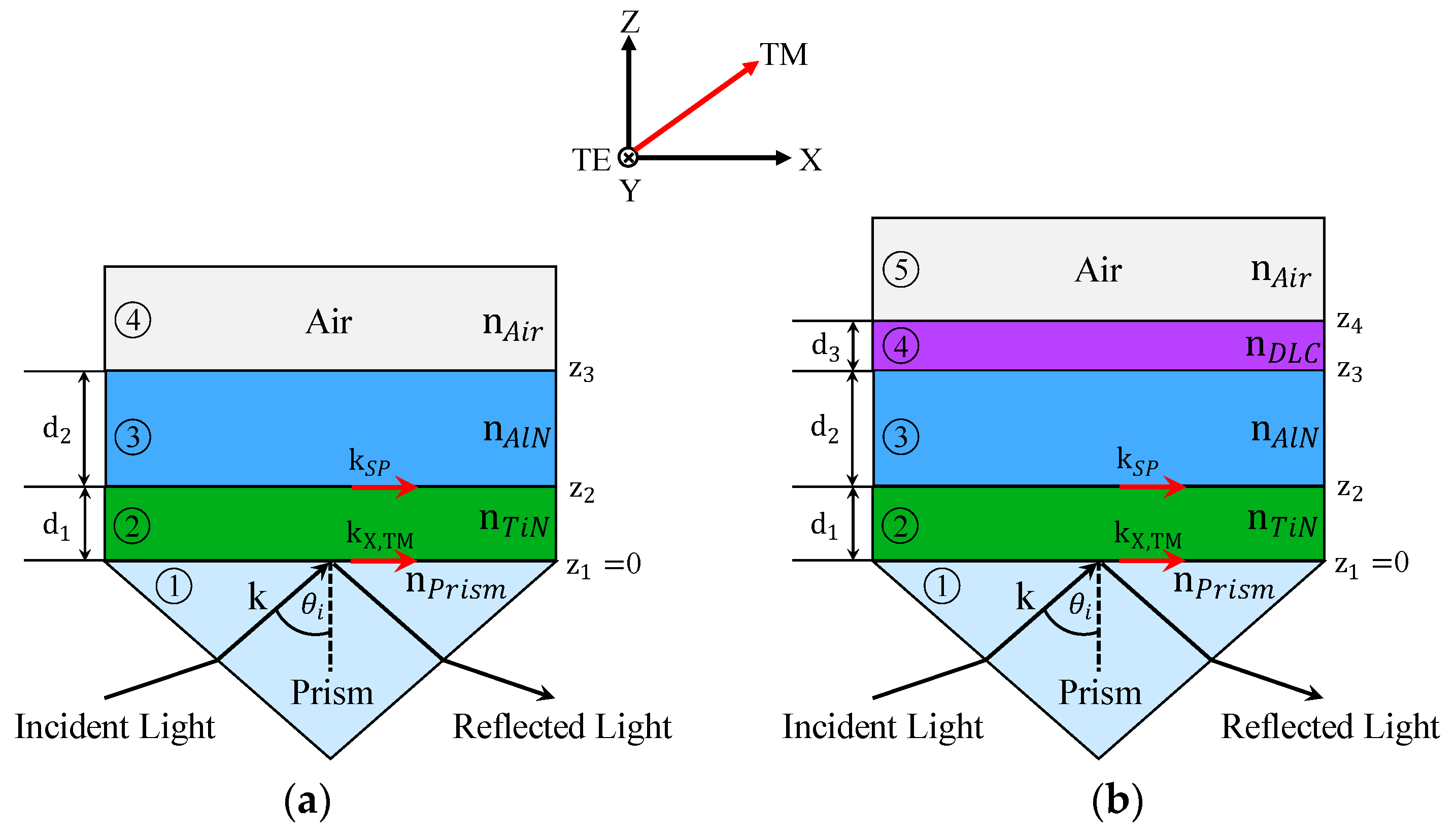
Figure 1. The schematic diagram shows the CPWR structures without a thin DLC film (a) and with a thin DLC film to be analyzed (b).
Photonics 09 00332 g001
Figure 2. The theoretical plots of the reflectivity versus incident angle for TM (red) and TE (blue) polarized incident light of the GA–optimized CPWR structures: (a) sapphire prism/29.42 nm TiN/909.83 nm AlN/air, (b) magnesium oxide prism/28.33 nm TiN/909.50 nm AlN/air, and (c) silicon prism/28.33 nm TiN/711.88 nm AlN/air.
Photonics 09 00332 g002
Figure 3. The electric field intensity for TM–polarized light for: (a) the sapphire prism/29.42 nm TiN/ 909.83 nm AlN/air sensor for incident angles of 35.91° (dash line) and 76.50° (solid line), (b) the magnesium oxide prism/28.33 nm TiN/ 909.50 nm AlN/air sensor for incident angles of 35.91° (dash line) and 76.50° (solid line), and (c) the silicon prism/28.33 nm TiN/ 711.88 nm AlN/air sensor for incident angles of 35.91° (dash line) and 76.50° (solid line).
Photonics 09 00332 g003
Figure 4. The calculated penetration depth (dp) for TM–polarized light for the GA–optimized sapphire (Al2O3) prism/TiN/AlN/air, magnesium oxide (MgO) prism/TiN/AlN/air, and silicon (Si) prism/TiN/AlN/air sensors was 181 nm, 182 nm, and 136 nm, respectively.
Photonics 09 00332 g004
Figure 5. The magnetic field distribution for TE–polarized light for: (a) the sapphire prism/29.42 nm TiN/909.83 nm AlN/air sensor for an incident angle of 57.06°, (b) the magnesium oxide prism/28.33 nm TiN/ 909.50 nm AlN/air sensor for an incident angle of 58.77°, and (c) the silicon/28.33 nm TiN/ 711.88 nm AlN/air sensor for incident angles of 19.35° (solid line) and 31.77° (dash line).
Photonics 09 00332 g005
Figure 6. Calculated reflectivity spectra for TM-polarized incident light of the optimized (a) sapphire prism/TiN/AlN/air sensor, (b) magnesium oxide prism/TiN/AlN/air sensor, and (c) silicon prism/TiN/AlN/air sensor, showing the shifts in reflectivity minima caused by deposition of DLC film thicknesses of 1–10 nm in steps of 1 nm.
Photonics 09 00332 g006
Figure 7. Calculated reflectivity spectra for TE-polarized incident light of the optimized (a) sapphire prism/TiN/AlN/air sensor, (b) magnesium oxide prism/TiN/AlN/air sensor, and (c,d) silicon prism/TiN/AlN/air sensor, showing the shifts in reflectivity minima caused by deposition of DLC films thicknesses of 1–10 nm in steps of 1 nm.
Photonics 09 00332 g007
Figure 8. Sensitivity curves as a function of the DLC thickness for the optimized CPWR sensors: (a) sapphire prism/TiN/AlN/air, (b) magnesium oxide prism/TiN/AlN/air, and (c) silicon prism/TiN/AlN/air.
Photonics 09 00332 g008
Figure 9. Sensitivity curves as a function of the RI of DLC films for the optimized CPWR sensors: (a) sapphire prism/TiN/AlN/air, (b) magnesium oxide prism/TiN/AlN/air, and (c) silicon prism/TiN/AlN/air.
Photonics 09 00332 g009
Figure 10. Examples of trial curves for simultaneous determination of the thickness and RI of DLC films using the graphical method for the sapphire prism/29.42 nm TiN/909.83 nm AlN sensor.
Photonics 09 00332 g010
Table 1. Summary of parameters used for simulation the CPWR sensors at 1550 nm.
LayerMaterialRefractive Index
PrismSapphire1.746 [51]
Silicon3.48 [28]
Magnesium oxide1.715 [52]
Plasmon activeTitanium nitride0.9857 + 9.1899i [29]
WaveguideAluminum nitride2.0293 + 0.0001i [53]
SensingDimond-like carbon1.79 + 0.0099i [54]
SurroundingAir1.00002 [54]
Table 2. The optimum of the TiN and AlN layer thicknesses of three CPWR sensors, predicted by GA method.
StructureThickness
TiN LayerAlN Layer
sapphire prism/TiN/AlN/air29.42 nm909.83 nm
magnesium oxide-prism/TiN/AlN/air28.33 nm909.50 nm
silicon prism/TiN/AlN/air28.33 nm771.88 nm
Table 3. The advantages and disadvantages of methods for simultaneous measurement of the thickness and RI of thin films.
Method AdvantageDisadvantage
Conventional SPR: prism/metal/airOne wavelength
[64,65]
-
high sensitivity
-
simple for fabrication
-
sharp resonance
-
thickness and refractive index cannot be determined from single measurement
-
incompatibility with CMOS fabrication processes
Two-color [66]
Three-wavelength [67]
-
thickness and refractive index can be determined from single measurement
-
dispersion function of the thin films must be known
Two-medium [60]
-
thin films being measured must have no interaction with the media
Optical fiber SPR: SiO2/Au/waterOne wavelength [6]
-
simple for fabrication
-
sharp resonance
-
compact size
-
cheap
-
thickness and refractive index cannot be determined from single measurement
Conventional CPWR:
prism/Au/SiO2/air
One wavelength
[15,16,17,18]
-
thickness and refractive index can be determined from single measurement
-
poor thermal stability
-
incompatibility with CMOS fabrication processes
Proposed CPWR:
prism/TiN/AlN/air
One wavelength
-
thickness and refractive index can be determined from single measurement
-
compatibility with CMOS fabrication process
-
wider and shallower resonance
-
more sensitive to noise
Ellipsometry
[62,63]
Multi wavelength
-
able to detect ultrathin layers
-
required complicate model
-
samples must be prepared
-
slow and difficult
-
expensive
Interferometry
[68]
One wavelength
-
low detection limits
-
high accuracy
-
large size, cumbersome
-
required system calibration
Publisher’s Note: MDPI stays neutral with regard to jurisdictional claims in published maps and institutional affiliations.