Total Internal Reflection Lens for Optical Wireless Receivers

 , , and
Abstract
:1. Introduction
2. Concept, Design, and Assembly
2.1. Concept
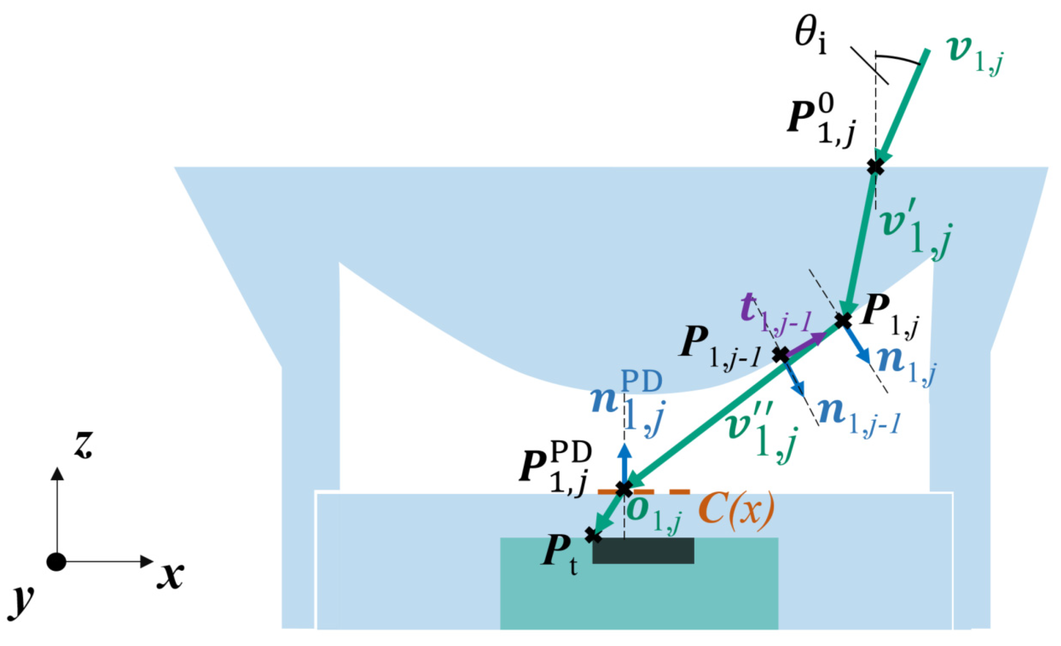
2.2. Geometrical Construction
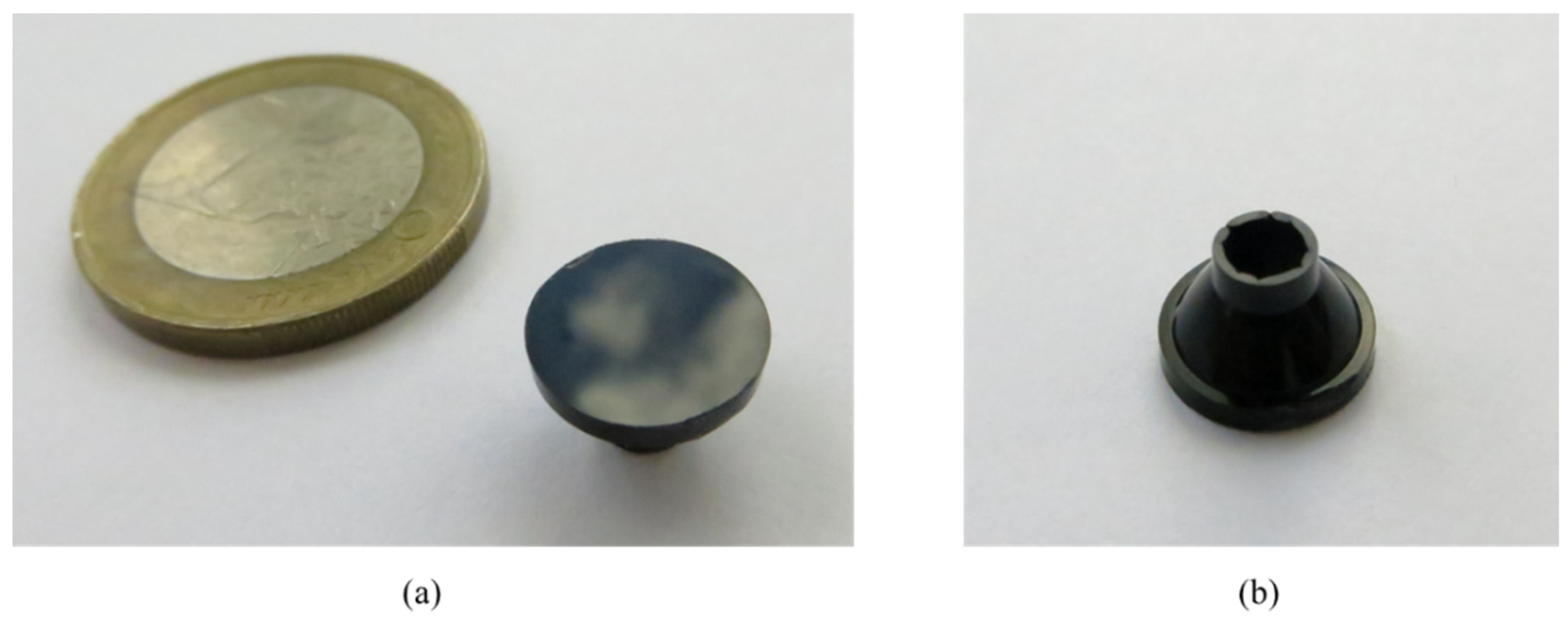
2.3. Frabication and Assembly
3. Measurements
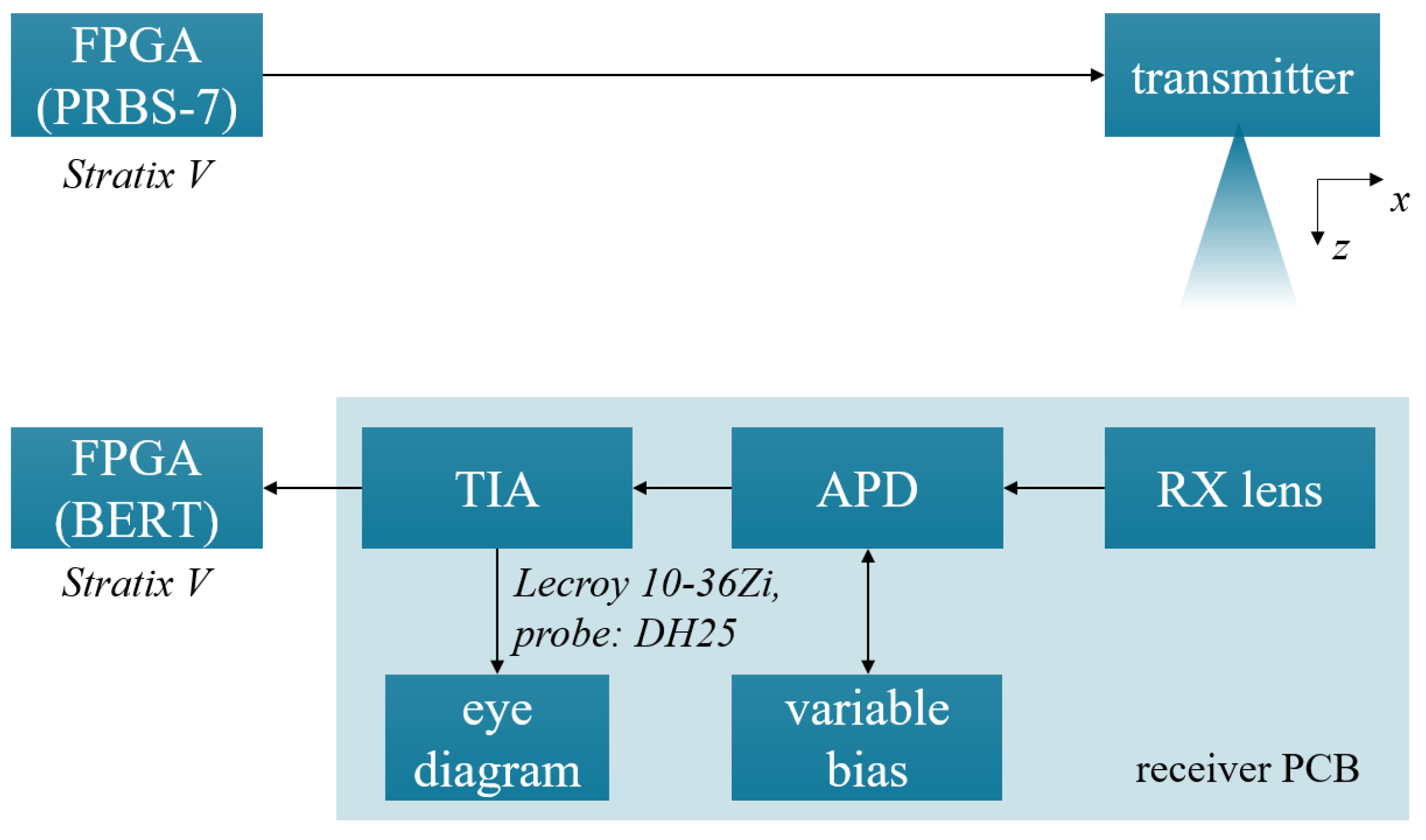
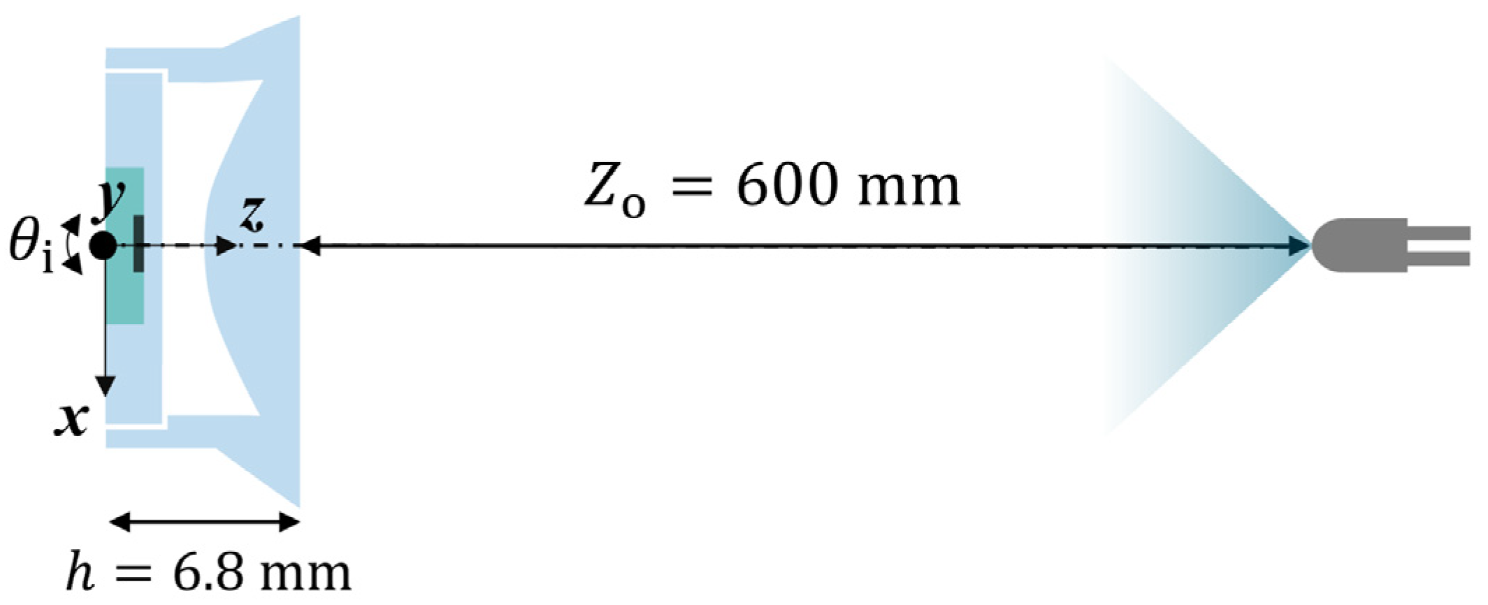
3.1. Optical Setup
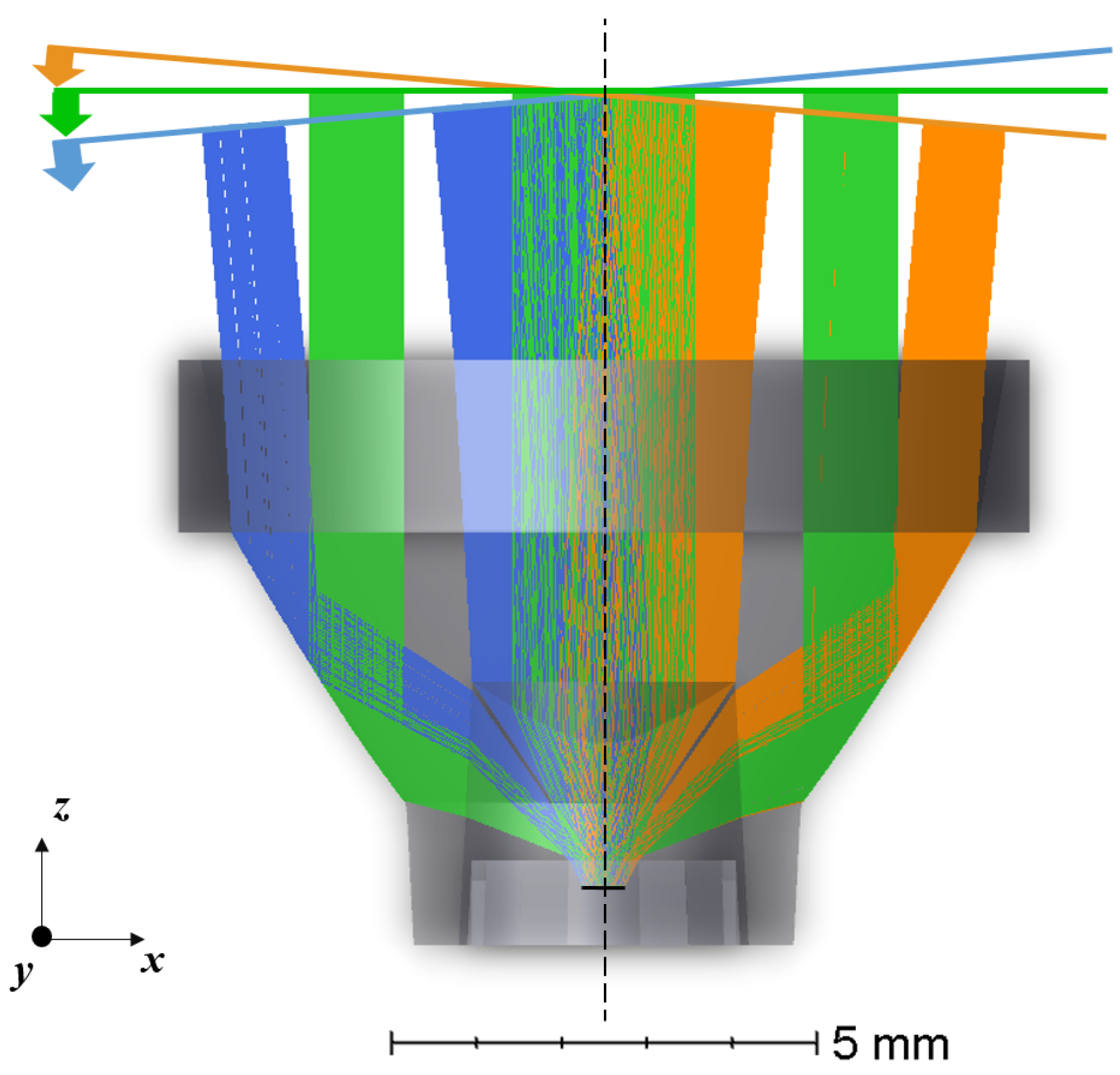
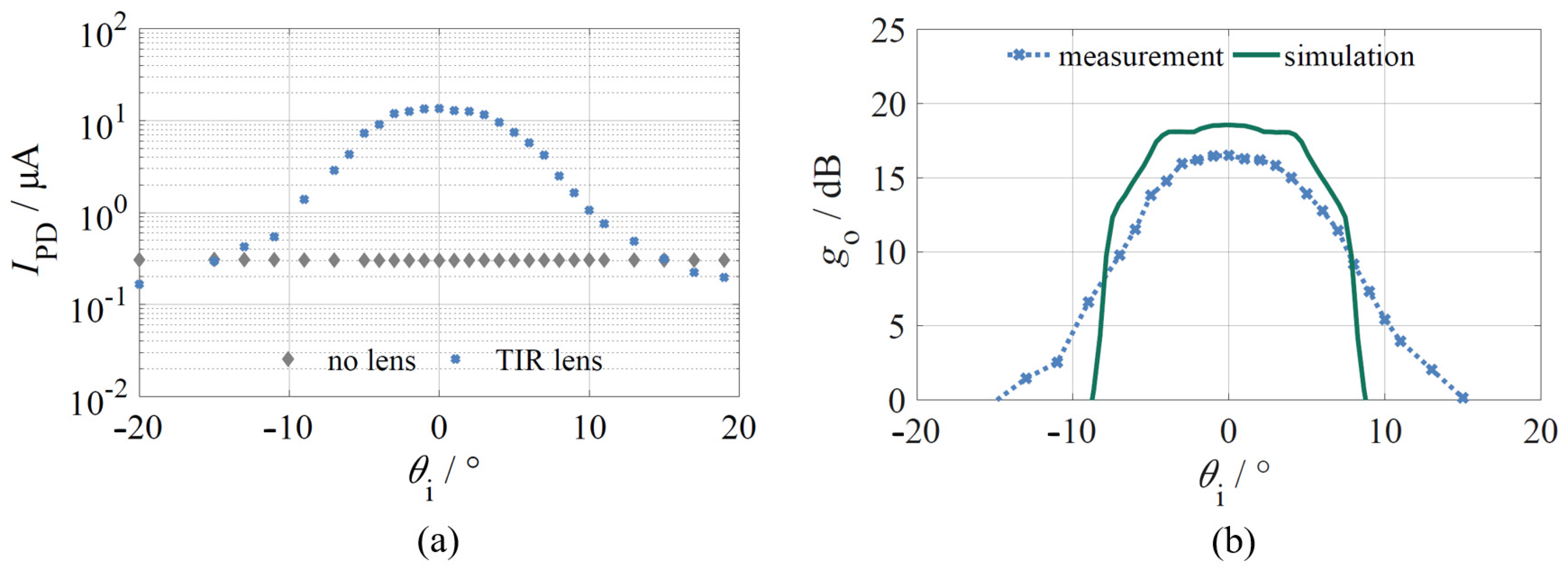
3.2. Optical Results
3.3. Data Transmission Setup
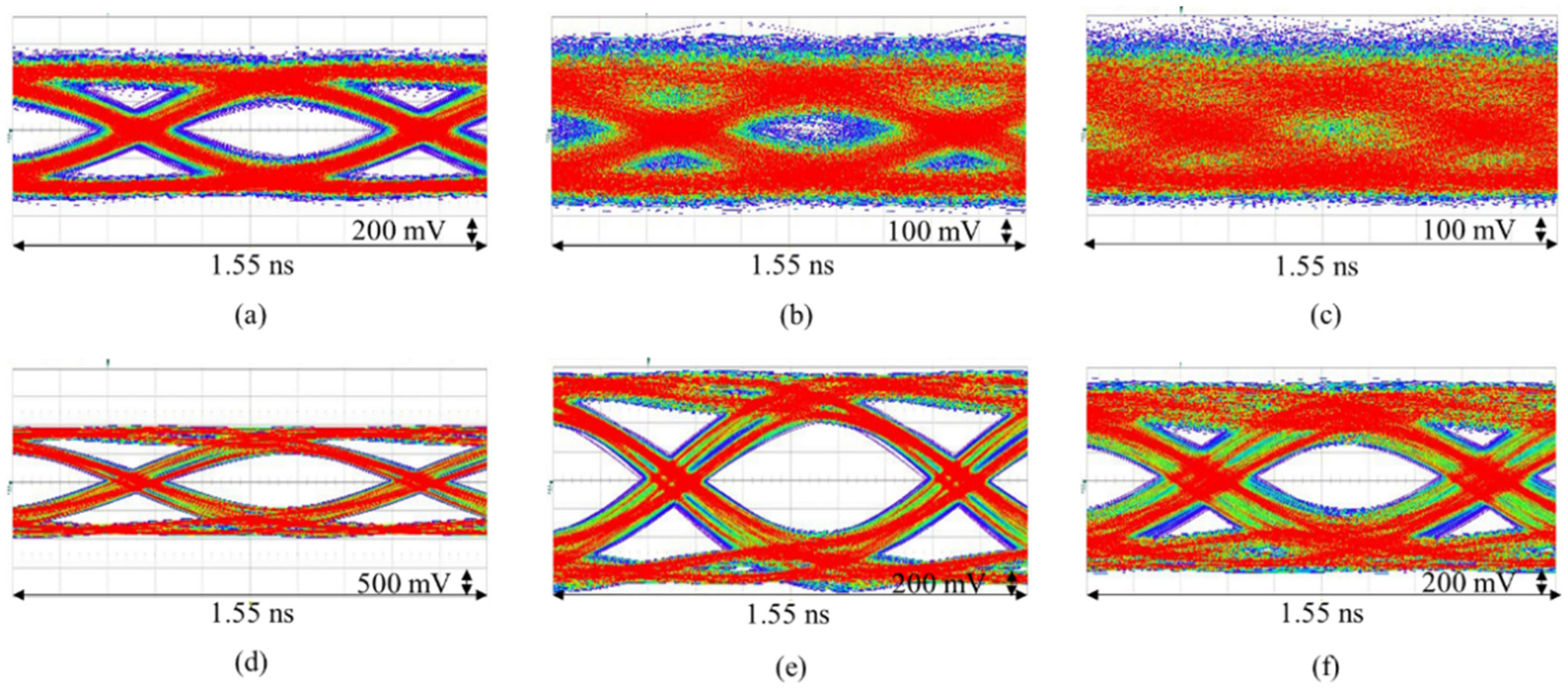
3.4. Data Transmission Results
4. Discussion
4.1. Performance
4.2. Comparison with CPC and DTIRC
5. Conclusions
Author Contributions
Funding
Institutional Review Board Statement
Informed Consent Statement
Data Availability Statement
Conflicts of Interest
References
- Winzer, P.J.; Neilson, D.T. From Scaling Disparities to Integrated Parallelism: A Decathlon for a Decade. J. Lightwave Technol. 2017, 35, 1099–1115. [Google Scholar] [CrossRef]
- Cerwall, P.; Ramiro, J.; Outes, J.; Bhardwaj, A.; Muñiz Garcia, C.; Baur, H.; Alger, J.; Krautkremer, T.; Chandra, R.; Lundborg, T.; et al. Ericsson Mobility Report: June 2021. Available online: https://www.ericsson.com/49cd40/assets/local/mobility-report/documents/2021/june-2021-ericsson-mobility-report.pdf (accessed on 16 June 2021).
- Fitzek, F.H.P.; Li, S.-C.; Speidel, S.; Strufe, T.; Simsek, M. (Eds.) Tactile Internet: With Human-In-the-Loop; Elsevier AP Academic Press: Cambridge, MA, USA, 2021; ISBN 0-12-821343-4. [Google Scholar]
- Szabo, D.; Gulyas, A.; Fitzek, F.H.P.; Lucani, D.E. Towards the Tactile Internet: Decreasing Communication Latency with Network Coding and Software Defined Networking. In Proceedings of the European Wireless 2015; 21th European Wireless Conference, Budapest, Hungary, 20–22 May 2015; pp. 1–6. [Google Scholar]
- Brandl, P.; Zimmermann, H. Optoelectronic integrated circuit for indoor optical wireless communication with adjustable beam. In Proceedings of the 2013 18th European Conference on Network and Optical Communications & 2013 8th Conference on Optical Cabling and Infrastructure (NOC-OC&I), Graz, Austria, 10–12 July 2013; pp. 149–152. [Google Scholar]
- O’Brien, D.; Turnbull, R.; Le Minh, H.; Faulkner, G.; Bouchet, O.; Porcon, P.; El Tabach, M.; Gueutier, E.; Wolf, M.; Grobe, L.; et al. High-Speed Optical Wireless Demonstrators: Conclusions and Future Directions. J. Lightwave Technol. 2012, 30, 2181–2187. [Google Scholar] [CrossRef] [Green Version]
- Chun, H.; Rajbhandari, S.; Tsonev, D.; Faulkner, G.; Haas, H.; O’Brien, D. Visible light communication using laser diode based remote phosphor technique. In Proceedings of the 2015 IEEE International Conference on Communication Workshop (ICCW), London, UK, 8–12 June 2015; pp. 1392–1397, ISBN 2164-7038. [Google Scholar]
- Yeh, C.-H.; Lu, I.-C. 0.52–11.86 Gbit/s OFDM modulation for power-sharing VLC transmission by using VCSEL laser. Opt. Express 2016, 24, 21113–21118. [Google Scholar] [CrossRef] [PubMed]
- Li, X.; Bamiedakis, N.; Guo, X.; McKendry, J.J.D.; Xie, E.; Ferreira, R.; Gu, E.; Dawson, M.D.; Penty, R.V.; White, I.H. Wireless Visible Light Communications Employing Feed-Forward Pre-Equalization and PAM-4 Modulation. J. Lightwave Technol. 2016, 34, 2049–2055. [Google Scholar] [CrossRef]
- Hussein, A.F.; Elgala, H.; Fahs, B.; Hella, M.M. Experimental investigation of DCO-OFDM adaptive loading using Si PN-based receiver. In Proceedings of the 2017 26th Wireless and Optical Communication Conference (WOCC), Newark, NJ, USA, 7–8 April 2017; ISBN 978-1-5090-4909-7. [Google Scholar]
- Yu, B.; Liang, S.; Ding, X.; Yang, Y.; Shao, C.; Zhao, Q.; Li, Z. Performance Investigation on Hemispherical Lens used in Photodetector for Visible Light Communications. In Proceedings of the 2019 20th International Conference on Electronic Packaging Technology(ICEPT), Hong Kong, China, 12–15 August 2019; pp. 1–4, ISBN 978-1-7281-5064-2. [Google Scholar]
- Faulwaßer, M.; Deicke, F.; Schneider, T. 10 Gbit/s bidirectional optical wireless communication module for docking devices. In Proceedings of the 2014 IEEE Globecom Workshops (GC Wkshps), Austin, TX, USA, 8–12 December 2014; pp. 512–517, ISBN 2166-0077. [Google Scholar]
- Wang, Y.; Lan, T.; Ni, G. Optical receiving system based on a compound parabolic concentrator and a hemispherical lens for visible light communication. Appl. Opt. 2016, 55, 10229–10238. [Google Scholar] [CrossRef]
- Kahn, J.M.; Barry, J.R. Wireless Infrared Communications. Proc. IEEE 1997, 85, 265–298. [Google Scholar] [CrossRef] [Green Version]
- Ramirez-Iniguez, R.; Idrus, S.M.; Sun, Z. Optical Wireless Communications: IR for Wireless Connectivity; Auerbach Publications: Boca Raton, FL, USA, 2008; ISBN 978-0367452674. [Google Scholar]
- Winston, R.; Miñano, J.C.; Benítez, P. Nonimaging Optics; Elsevier Academic: Amsterdam, The Netherlands, 2005; ISBN 9780127597515. [Google Scholar]
- Collins, S.; O’Brien, D.C.; Watt, A. High gain, wide field of view concentrator for optical communications. Opt. Lett. 2014, 39, 1756–1759. [Google Scholar] [CrossRef]
- Collins, S.; Mulyawan, R.; Rajbhandari, S.; Chu, H.; Faulkner, G.E.; O’Brien, D.C.; Manousiadis, P.P.; Vithanage, D.A.; Turnbull, G.A.; Samuel, I.D.W. A simple wide field of view concentrator for free space visible light communications. In Proceedings of the 2015 IEEE Photonics Society Summer Topical Meeting Series (SUM), Nassau, Bahamas, 13–15 July 2015; pp. 43–44, ISBN 978-1-4799-7468-9. [Google Scholar]
- Collins, S. Smart Phones: An example application for fluorescent concentrators. In Proceedings of the 2019 Global LIFI Congress (GLC), Paris, France, 12–13 June 2019; pp. 1–4, ISBN 978-1-7281-5022-2. [Google Scholar]
- Manousiadis, P.P.; Rajbhandari, S.; Mulyawan, R.; Vithanage, D.A.; Chun, H.; Faulkner, G.; O’Brien, D.C.; Turnbull, G.A.; Collins, S.; Samuel, I.D. Wide field-of-view fluorescent antenna for visible light communications beyond the étendue limit. Optica 2016, 3, 702. [Google Scholar] [CrossRef]
- Peyronel, T.; Quirk, K.J.; Wang, S.C.; Tiecke, T.G. Luminescent detector for free-space optical communication. Optica 2016, 3, 787. [Google Scholar] [CrossRef]
- Yu, B.; Liang, S.; Ding, X.; Li, Z.; Tang, Y. A Sandwich Structure Light-Trapping Fluorescence Antenna With Large Field of View for Visible Light Communication. IEEE Trans. Electron Devices 2021, 68, 565–571. [Google Scholar] [CrossRef]
- Portnoi, M.; Haigh, P.A.; Macdonald, T.J.; Ambroz, F.; Parkin, I.P.; Darwazeh, I.; Papakonstantinou, I. Bandwidth limits of luminescent solar concentrators as detectors in free-space optical communication systems. Light Sci. Appl. 2021, 10, 3. [Google Scholar] [CrossRef] [PubMed]
- Ning, X.; Winston, R.; O’Gallagher, J. Dielectric totally internally reflecting concentrators. Appl. Opt. 1987, 26, 300–305. [Google Scholar] [CrossRef] [PubMed]
- Garcia-Marquez, J.; Valencia, J.C.; Perez, H.; Topsu, S. Catadioptric lenses in Visible Light Communications. J. Phys. Conf. Ser. 2015, 605, 12029. [Google Scholar] [CrossRef] [Green Version]
- García-Márquez, J.; Valencia-Estrada, C.; Topsu, S.; Chassagne, L. Optical antenna for a visible light communications receiver. In Broadband Access Communication Technologies XII, Proceedings of SPIE Volume 10559, San Francisco, CA, USA, 27 January–1 February 2018; Dingel, B.B., Tsukamoto, K., Mikroulis, S., Eds.; SPIE: Bellingham, WA, USA, 2018; p. 20. ISBN 9781510616035. [Google Scholar]
- Chen, T.; Liu, L.; Tu, B.; Zheng, Z.; Hu, W. High-Spatial-Diversity Imaging Receiver Using Fisheye Lens for Indoor MIMO VLCs. IEEE Photon. Technol. Lett. 2014, 26, 2260–2263. [Google Scholar] [CrossRef]
- Tang, X.; Pan, D.; Zhang, X.; Xi, L.; Zhang, W. A novel receiver employing a compound-eye lens and a frequency domain synchronization algorithm for multiple-input single-output visible light communication system. In Proceedings of the 2015 14th International Conference on Optical Communications and Networks (ICOCN), Nanjing, China, 3–5 July 2015; ISBN 978-1-4673-7373-9. [Google Scholar]
- Faulwaßer, M.; Kirrbach, R.; Schneider, T.; Noack, A. 10 Gbit/s bidirectional transceiver with monolithic optic for rotary connector replacements. In Proceedings of the 2018 Global LIFI Congress, Paris, France, 8–9 February 2018; pp. 95–102. [Google Scholar]
- Kirrbach, R.; Faulwaßer, M.; Schneider, T.; Meißner, P.; Noack, A.; Deicke, F. Monolitic Hybrid Transmitter-Receiver Lens for Rotary On-Axis Communications. Appl. Sci. 2020, 10, 1540. [Google Scholar] [CrossRef] [Green Version]
- Kirrbach, R.; Jakob, B.; Noack, A. Introducing Advanced Freeform Optic Design to Li-Fi Technology. In Proceedings of the 7th International Conference on Photonics, Optics and Laser Technology, Prague, Czech Republic, 25–27 February 2019; pp. 2184–4364. [Google Scholar] [CrossRef]
- Wallhead, I.; Jiménez, T.M.; Ortiz, J.V.G.; Toledo, I.G.; Toledo, C.G. Design of an efficient Fresnel-type lens utilizing double total internal reflection for solar energy collection. Opt. Express 2012, 20, A1005–A1010. [Google Scholar] [CrossRef] [PubMed]
- Säckinger, E. Analysis and Design of Transimpedance Amplifiers for Optical Receivers; John Wiley & Sons, Inc.: Hoboken, NJ, USA, 2017; ISBN 9781119264422. [Google Scholar]


| Parameter | Symbol | Value | Unit |
|---|---|---|---|
| Wavelength | 850 | nm | |
| Calculated points | N | 1200 | per surface |
| PD | - | Si-APD | - |
| PD diameter | dPD | 0.5 | mm |
| Responsivity (M = 1) | R | 0.5 | A/W |
| Lens input diameter | dl | 8.8 | mm |
| Acceptance angle | ±5 | ° | |
| Calculated points | N | 1200 | per surface |
| Bit rate | R | 1.289 | Gbit/s |
| Modulation | - | NRZ-OOK | - |
| Pattern | - | PRBS-7 | - |
| Probe bandwidth | fprobe | 13 | GHz |
| Configuration | TIR Lens | Zo | BER |
|---|---|---|---|
| a | no | 50 cm | <10−12 |
| b | no | 100 cm | 3 × 10⁻⁴ |
| c | no | 150 cm | 3 × 10⁻² |
| d | yes | 50 cm | <10−12 |
| e | yes | 100 cm | <10−12 |
| f | yes | 150 cm | <10−12 |
Publisher’s Note: MDPI stays neutral with regard to jurisdictional claims in published maps and institutional affiliations. |
© 2022 by the authors. Licensee MDPI, Basel, Switzerland. This article is an open access article distributed under the terms and conditions of the Creative Commons Attribution (CC BY) license (https://creativecommons.org/licenses/by/4.0/).
Share and Cite
Kirrbach, R.; Schneider, T.; Stephan, M.; Noack, A.; Faulwaßer, M.; Deicke, F. Total Internal Reflection Lens for Optical Wireless Receivers. Photonics 2022, 9, 276. https://doi.org/10.3390/photonics9050276
Kirrbach R, Schneider T, Stephan M, Noack A, Faulwaßer M, Deicke F. Total Internal Reflection Lens for Optical Wireless Receivers. Photonics. 2022; 9(5):276. https://doi.org/10.3390/photonics9050276
Chicago/Turabian StyleKirrbach, René, Tobias Schneider, Mira Stephan, Alexander Noack, Michael Faulwaßer, and Frank Deicke. 2022. "Total Internal Reflection Lens for Optical Wireless Receivers" Photonics 9, no. 5: 276. https://doi.org/10.3390/photonics9050276
APA StyleKirrbach, R., Schneider, T., Stephan, M., Noack, A., Faulwaßer, M., & Deicke, F. (2022). Total Internal Reflection Lens for Optical Wireless Receivers. Photonics, 9(5), 276. https://doi.org/10.3390/photonics9050276